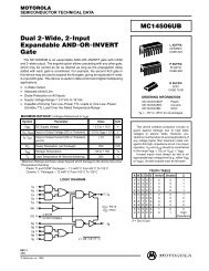
74ALS157/74ALS158 Data selector/multiplexer
74ALS157/74ALS158 Data selector/multiplexer
74ALS157/74ALS158 Data selector/multiplexer

You also want an ePaper? Increase the reach of your titles
YUMPU automatically turns print PDFs into web optimized ePapers that Google loves.
INTEGRATED CIRCUITS<br />
<strong>74ALS157</strong>/<strong>74ALS158</strong><br />
<strong>Data</strong> <strong>selector</strong>/<strong>multiplexer</strong><br />
Product specification<br />
IC05 <strong>Data</strong> Handbook<br />
1991 Feb 08
Philips Semiconductors<br />
Product specification<br />
<strong>Data</strong> <strong>selector</strong>/<strong>multiplexer</strong><br />
<strong>74ALS157</strong>/<strong>74ALS158</strong><br />
<strong>74ALS157</strong> Quad 2-input data <strong>selector</strong>/<strong>multiplexer</strong>, non-inverting<br />
<strong>74ALS158</strong> Quad 2-input data <strong>selector</strong>/<strong>multiplexer</strong>, inverting<br />
DESCRIPTION<br />
The <strong>74ALS157</strong> is a quad 2-input <strong>multiplexer</strong> which selects 4 bits of<br />
data from one of two sources under the control of a common select<br />
input (S). The enable input (E) is active when Low. When E is High,<br />
all of the outputs (Yn) are forced Low regardless of all other input<br />
conditions.<br />
Moving data from two registers to a common output bus is a typical<br />
use of the <strong>74ALS157</strong>. The state of the select input determines the<br />
particular register from which data comes.<br />
The device is the logic implementation of 4-pole, 2-position switch<br />
where the position of the switch is determined by the logic levels<br />
supplied to the select input. The <strong>74ALS158</strong> is similar but has<br />
inverting outputs (Yn).<br />
TYPE<br />
TYPICAL<br />
PROPAGATION DELAY<br />
TYPICAL<br />
SUPPLY CURRENT<br />
(TOTAL)<br />
<strong>74ALS157</strong> 6.0ns 6mA<br />
<strong>74ALS158</strong> 6.0ns 6mA<br />
ORDERING INFORMATION<br />
DESCRIPTION<br />
ORDER CODE<br />
COMMERCIAL RANGE<br />
V CC = 5V ±10%,<br />
T amb = 0°C to +70°C<br />
DRAWING<br />
NUMBER<br />
16-pin plastic DIP <strong>74ALS157</strong>N, <strong>74ALS158</strong>N SOT38-4<br />
16-pin plastic SO <strong>74ALS157</strong>D, <strong>74ALS158</strong>D SOT109-1<br />
INPUT AND OUTPUT LOADING AND FAN-OUT TABLE<br />
NOTE:<br />
PINS<br />
DESCRIPTION<br />
74ALS (U.L.)<br />
HIGH/LOW<br />
LOAD VALUE<br />
HIGH/LOW<br />
Ina, Inb, Inc, Ind <strong>Data</strong> inputs 1.0/1.0 20µA/0.1mA<br />
S Select input 1.0/1.0 20µA/0.1mA<br />
E Enable input 1.0/1.0 20µA/0.1mA<br />
Ya – Yd, Ya – Yd <strong>Data</strong> outputs 20/240 0.4mA/24mA<br />
One (1.0) ALS unit load is defined as: 20µA in the High state and 0.1mA in the Low state.<br />
PIN CONFIGURATION – <strong>74ALS157</strong><br />
PIN CONFIGURATION – <strong>74ALS158</strong><br />
S<br />
1<br />
16<br />
V CC<br />
S<br />
1<br />
16<br />
V CC<br />
I0a<br />
2<br />
15<br />
E<br />
I0a<br />
2<br />
15<br />
E<br />
I1a<br />
3<br />
14<br />
I0d<br />
I1a<br />
3<br />
14<br />
I0d<br />
Ya<br />
4<br />
13<br />
I1d<br />
Ya<br />
4<br />
13<br />
I1d<br />
I0b<br />
5<br />
12<br />
Yd<br />
I0b<br />
5<br />
12<br />
Yd<br />
I1b<br />
6<br />
11<br />
I0c<br />
I1b<br />
6<br />
11<br />
I0c<br />
Yb<br />
7<br />
10<br />
I1c<br />
Yb<br />
7<br />
10<br />
I1c<br />
GND<br />
8<br />
9<br />
Yc<br />
GND<br />
8<br />
9<br />
Yc<br />
SC00051<br />
SC00052<br />
LOGIC SYMBOL – <strong>74ALS157</strong><br />
LOGIC SYMBOL – <strong>74ALS158</strong><br />
2 3 5 6 11 10 14<br />
13<br />
2 3 5 6 11 10 14<br />
13<br />
I0a I1a I0b I1b I0c I1c I0d<br />
I1d<br />
I0a I1a I0b I1b I0c I1c I0d I1d<br />
1<br />
S<br />
1<br />
S<br />
15<br />
E<br />
15<br />
E<br />
Ya Yb Yc Yd<br />
Ya Yb Yc Yd<br />
V CC = Pin 16<br />
GND = Pin 8<br />
4 7 9 12<br />
SC00053<br />
V CC = Pin 16<br />
GND = Pin 8<br />
4 7 9 12<br />
SC00054<br />
1991 Feb 08 2<br />
853–1129 01670
Philips Semiconductors<br />
<strong>Data</strong> <strong>selector</strong>/<strong>multiplexer</strong><br />
Product specification<br />
<strong>74ALS157</strong>/<strong>74ALS158</strong><br />
IEC/IEEE SYMBOL – <strong>74ALS157</strong><br />
IEC/IEEE SYMBOL – <strong>74ALS158</strong><br />
1<br />
15<br />
G1<br />
EN<br />
1<br />
15<br />
G1<br />
EN<br />
2<br />
3<br />
5<br />
6<br />
1<br />
1<br />
MUX<br />
4<br />
7<br />
2<br />
3<br />
5<br />
6<br />
1<br />
1<br />
MUX<br />
4<br />
7<br />
11<br />
10<br />
9<br />
11<br />
10<br />
9<br />
14<br />
13<br />
12<br />
14<br />
13<br />
12<br />
SC00055<br />
SC00056<br />
LOGIC DIAGRAM – <strong>74ALS157</strong><br />
E I0a I1a I0b I1b I0c I1c I0d I0d S<br />
15 2 3 5 6 11 10 14 13 1<br />
LOGIC DIAGRAM – <strong>74ALS158</strong><br />
E I0a I1a I0b I1b I0c I1c I0d I0d S<br />
15 2 3 5 6 11 10 14 13 1<br />
4 7 9 12<br />
Ya Yb Yc Yd<br />
4 7 9 12<br />
Ya Yb Yc Yd<br />
V CC = Pin 16<br />
GND = Pin 8<br />
SC00057<br />
V CC = Pin 16<br />
GND = Pin 8<br />
SC00058<br />
FUNCTION TABLE – <strong>74ALS157</strong><br />
INPUTS<br />
OUTPUTS<br />
E S I0n I1n Yn<br />
H X X X L<br />
L L L X L<br />
L L H X H<br />
L H X L L<br />
L H X H H<br />
H = High voltage level<br />
L = Low voltage level<br />
X = Don’t care<br />
FUNCTION TABLE – <strong>74ALS158</strong><br />
INPUTS<br />
OUTPUTS<br />
E S I0n I1n Yn<br />
H X X X H<br />
L L L X H<br />
L L H X L<br />
L H X L H<br />
L H X H L<br />
H = High voltage level<br />
L = Low voltage level<br />
X = Don’t care<br />
1991 Feb 08 3
Philips Semiconductors<br />
<strong>Data</strong> <strong>selector</strong>/<strong>multiplexer</strong><br />
Product specification<br />
<strong>74ALS157</strong>/<strong>74ALS158</strong><br />
ABSOLUTE MAXIMUM RATINGS<br />
(Operation beyond the limit set forth in this table may impair the useful life of the device.<br />
Unless otherwise noted these limits are over the operating free-air temperature range.)<br />
SYMBOL PARAMETER RATING UNIT<br />
V CC Supply voltage –0.5 to +7.0 V<br />
V IN Input voltage –0.5 to +7.0 V<br />
I IN Input current –30 to +5 mA<br />
V OUT Voltage applied to output in High output state –0.5 to V CC V<br />
I OUT Current applied to output in Low output state 16 mA<br />
T amb Operating free-air temperature range 0 to +70 °C<br />
T stg Storage temperature range –65 to +150 °C<br />
RECOMMENDED OPERATING CONDITIONS<br />
SYMBOL<br />
PARAMETER<br />
LIMITS<br />
MIN NOM MAX<br />
V CC Supply voltage 4.5 5.0 5.5 V<br />
V IH High-level input voltage 2.0 V<br />
V IL Low-level input voltage 0.8 V<br />
I Ik Input clamp current –18 mA<br />
I OH High-level output current –0.4 mA<br />
I OL Low-level output current 8 mA<br />
T amb Operating free-air temperature range 0 +70 °C<br />
UNIT<br />
DC ELECTRICAL CHARACTERISTICS<br />
(Over recommended operating free-air temperature range unless otherwise noted.)<br />
SYMBOL PARAMETER TEST CONDITIONS 1 MIN TYP 2 MAX<br />
LIMITS<br />
UNIT<br />
V OH<br />
High-level output voltage<br />
V CC = ±10%, V IL = MAX,<br />
V IH = MIN<br />
I OH = MAX V CC – 2 V<br />
V = MIN, V = MAX, I OL = 4mA 0.25 0.40 V<br />
V OL Low-level output voltage CC IL V IH = MIN<br />
I OL = 8mA 0.35 0.50 V<br />
V IK Input clamp voltage V CC = MIN, I I = I IK –0.73 –1.5 V<br />
I I Input current at minimum input voltage V CC = MAX, V I = 7.0V 0.1 mA<br />
I IH High-level input current V CC = MAX, V I = 2.7V 20 µA<br />
I IL Low-level input current V CC = MAX, V I = 0.4V –0.1 mA<br />
I O Output current 3 V CC = MAX, V O = 2.25V –30 –112 mA<br />
I CC<br />
Supply current (total)<br />
<strong>74ALS157</strong><br />
<strong>74ALS158</strong><br />
V CC = MAX<br />
6 11 mA<br />
6 10 mA<br />
NOTES:<br />
1. For conditions shown as MIN or MAX, use the appropriate value specified under recommended operating conditions for the applicable type.<br />
2. All typical values are at V CC = 5V, T amb = 25°C.<br />
3. The output conditions have been chosen to produce a current that closely approximates one half of the true short-circuit output current, I OS .<br />
1991 Feb 08 4
Philips Semiconductors<br />
<strong>Data</strong> <strong>selector</strong>/<strong>multiplexer</strong><br />
Product specification<br />
<strong>74ALS157</strong>/<strong>74ALS158</strong><br />
AC ELECTRICAL CHARACTERISTICS<br />
SYMBOL PARAMETER TEST CONDITION<br />
LIMITS<br />
T amb = 0°C to +70°C<br />
V CC = +5.0V ± 10%<br />
C L = 50pF, R L = 500Ω<br />
UNIT<br />
MIN<br />
MAX<br />
t PLH<br />
t PHL<br />
Propagation delay<br />
I0n or I1n to Yn<br />
Waveform 1<br />
2.0<br />
2.0<br />
9.0<br />
9.0<br />
ns<br />
t PLH<br />
t PHL<br />
Propagation delay<br />
S to Yn<br />
<strong>74ALS157</strong> Waveform 1, 3<br />
4.0<br />
4.0<br />
12.0<br />
12.0<br />
ns<br />
t PLH<br />
t PHL<br />
Propagation delay<br />
E to Yn<br />
Waveform 3<br />
4.0<br />
7.0<br />
11.0<br />
14.0<br />
ns<br />
t PLH<br />
t PHL<br />
Propagation delay<br />
I0n or I1n to Yn<br />
Waveform 2<br />
2.0<br />
2.0<br />
8.0<br />
8.0<br />
ns<br />
t PLH<br />
t PHL<br />
Propagation delay<br />
S to Yn<br />
<strong>74ALS158</strong> Waveform 2, 4<br />
4.0<br />
4.0<br />
12.0<br />
12.0<br />
ns<br />
t PLH<br />
t PHL<br />
Propagation delay<br />
E to Yn<br />
Waveform 4<br />
4.0<br />
4.0<br />
14.0<br />
14.0<br />
ns<br />
AC WAVEFORMS<br />
For all waveforms, V M = 1.3V.<br />
I0n, I1n, S<br />
V M<br />
I0n, I1n, S<br />
V M<br />
t PLH<br />
V M<br />
V M V M<br />
t PHL<br />
V M<br />
V M V M<br />
t PHL<br />
t PLH<br />
Yn, Yn<br />
Yn, Yn<br />
SC00059<br />
SC00060<br />
Waveform 1.<br />
Propagation Delay for <strong>Data</strong> and Select to Output<br />
Waveform 2.<br />
Propagation Delay for <strong>Data</strong> and Select to Output<br />
E, S<br />
V M<br />
E, S<br />
V M<br />
t PLH<br />
V M<br />
V M V M<br />
t PHL<br />
V M<br />
V M V M<br />
t PHL<br />
t PLH<br />
Yn, Yn<br />
Yn, Yn<br />
SC00061<br />
SC00062<br />
Waveform 3.<br />
Propagation Delay for Enable and<br />
Select to Output<br />
Waveform 4.<br />
Propagation Delay for Enable and<br />
Select to Output<br />
1991 Feb 08 5
Philips Semiconductors<br />
Product specification<br />
<strong>Data</strong> <strong>selector</strong>/<strong>multiplexer</strong><br />
<strong>74ALS157</strong>/<strong>74ALS158</strong><br />
TEST CIRCUIT AND WAVEFORMS<br />
PULSE<br />
GENERATOR<br />
V IN<br />
V CC<br />
D.U.T.<br />
V OUT<br />
NEGATIVE<br />
PULSE<br />
90%<br />
V M<br />
10%<br />
t THL ( t ff)<br />
t w<br />
t TLH ( t r )<br />
V M<br />
10%<br />
90%<br />
AMP (V)<br />
0.3V<br />
R T<br />
C L R L<br />
Test Circuit for Totem-pole Outputs<br />
POSITIVE<br />
PULSE<br />
10%<br />
90%<br />
V M<br />
t TLH ( t r )<br />
t w<br />
t THL ( t f )<br />
90%<br />
V M<br />
10%<br />
AMP (V)<br />
0.3V<br />
DEFINITIONS:<br />
R L = Load resistor;<br />
see AC electrical characteristics for value.<br />
C L = Load capacitance includes jig and probe capacitance;<br />
see AC electrical characteristics for value.<br />
R T = Termination resistance should be equal to Z OUT of<br />
pulse generators.<br />
Family<br />
74ALS<br />
Input Pulse Definition<br />
INPUT PULSE REQUIREMENTS<br />
Amplitude V M<br />
3.5V 1.3V<br />
Rep.Rate t w t TLH t THL<br />
1MHz 500ns 2.0ns 2.0ns<br />
SC00005<br />
1991 Feb 08 6
Philips Semiconductors<br />
<strong>Data</strong> <strong>selector</strong>/<strong>multiplexer</strong><br />
Product specification<br />
<strong>74ALS157</strong>/<strong>74ALS158</strong><br />
DIP16: plastic dual in-line package; 16 leads (300 mil) SOT38-4<br />
1991 Feb 08 7
Philips Semiconductors<br />
<strong>Data</strong> <strong>selector</strong>/<strong>multiplexer</strong><br />
Product specification<br />
<strong>74ALS157</strong>/<strong>74ALS158</strong><br />
SO16: plastic small outline package; 16 leads; body width 3.9 mm SOT109-1<br />
1991 Feb 08 8
Philips Semiconductors<br />
<strong>Data</strong> <strong>selector</strong>/<strong>multiplexer</strong><br />
Product specification<br />
<strong>74ALS157</strong>/<strong>74ALS158</strong><br />
DEFINITIONS<br />
<strong>Data</strong> Sheet Identification Product Status Definition<br />
Objective Specification<br />
Preliminary Specification<br />
Product Specification<br />
Formative or in Design<br />
Preproduction Product<br />
Full Production<br />
This data sheet contains the design target or goal specifications for product development. Specifications<br />
may change in any manner without notice.<br />
This data sheet contains preliminary data, and supplementary data will be published at a later date. Philips<br />
Semiconductors reserves the right to make changes at any time without notice in order to improve design<br />
and supply the best possible product.<br />
This data sheet contains Final Specifications. Philips Semiconductors reserves the right to make changes<br />
at any time without notice, in order to improve design and supply the best possible product.<br />
Philips Semiconductors and Philips Electronics North America Corporation reserve the right to make changes, without notice, in the products,<br />
including circuits, standard cells, and/or software, described or contained herein in order to improve design and/or performance. Philips<br />
Semiconductors assumes no responsibility or liability for the use of any of these products, conveys no license or title under any patent, copyright,<br />
or mask work right to these products, and makes no representations or warranties that these products are free from patent, copyright, or mask<br />
work right infringement, unless otherwise specified. Applications that are described herein for any of these products are for illustrative purposes<br />
only. Philips Semiconductors makes no representation or warranty that such applications will be suitable for the specified use without further testing<br />
or modification.<br />
LIFE SUPPORT APPLICATIONS<br />
Philips Semiconductors and Philips Electronics North America Corporation Products are not designed for use in life support appliances, devices,<br />
or systems where malfunction of a Philips Semiconductors and Philips Electronics North America Corporation Product can reasonably be expected<br />
to result in a personal injury. Philips Semiconductors and Philips Electronics North America Corporation customers using or selling Philips<br />
Semiconductors and Philips Electronics North America Corporation Products for use in such applications do so at their own risk and agree to fully<br />
indemnify Philips Semiconductors and Philips Electronics North America Corporation for any damages resulting from such improper use or sale.<br />
Philips Semiconductors<br />
811 East Arques Avenue<br />
P.O. Box 3409<br />
Sunnyvale, California 94088–3409<br />
Telephone 800-234-7381<br />
© Copyright Philips Electronics North America Corporation 1997<br />
All rights reserved. Printed in U.S.A.<br />
<br />
<br />
1991 Feb 08 9