DATASHEET SEARCH SITE | WWW.ALLDATASHEET.COM
DATASHEET SEARCH SITE | WWW.ALLDATASHEET.COM
DATASHEET SEARCH SITE | WWW.ALLDATASHEET.COM

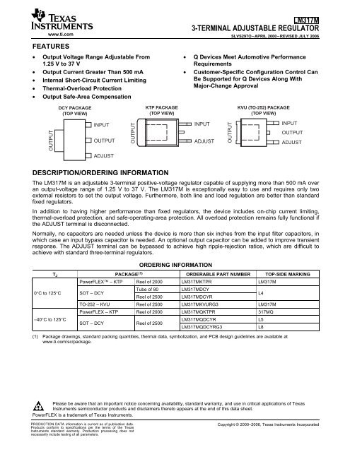
Create successful ePaper yourself
Turn your PDF publications into a flip-book with our unique Google optimized e-Paper software.
www.ti.comFEATURESLM317M3-TERMINAL ADJUSTABLE REGULATORSLVS297O–APRIL 2000–REVISED JULY 2006• Output Voltage Range Adjustable From • Q Devices Meet Automotive Performance1.25 V to 37 V Requirements• Output Current Greater Than 500 mA • Customer-Specific Configuration Control Can• Internal Short-Circuit Current LimitingBe Supported for Q Devices Along With• Thermal-Overload ProtectionMajor-Change Approval• Output Safe-Area CompensationDCY PACKAGE(TOP VIEW)KTP PACKAGE(TOP VIEW)KVU (TO-252) PACKAGE(TOP VIEW)OUTPUTINPUTOUTPUTOUTPUTINPUTADJUSTOUTPUTINPUTOUTPUTADJUSTADJUSTDESCRIPTION/ORDERING INFORMATIONThe LM317M is an adjustable 3-terminal positive-voltage regulator capable of supplying more than 500 mA overan output-voltage range of 1.25 V to 37 V. The LM317M is exceptionally easy to use and requires only twoexternal resistors to set the output voltage. Furthermore, both line and load regulation are better than standardfixed regulators.In addition to having higher performance than fixed regulators, the device includes on-chip current limiting,thermal-overload protection, and safe-operating-area protection. All overload protection remains fully functional ifthe ADJUST terminal is disconnected.Normally, no capacitors are needed unless the device is more than six inches from the input filter capacitors, inwhich case an input bypass capacitor is needed. An optional output capacitor can be added to improve transientresponse. The ADJUST terminal can be bypassed to achieve high ripple-rejection ratios, which are difficult toachieve with standard three-terminal regulators.ORDERING INFORMATIONT J PACKAGE (1) ORDERABLE PART NUMBER TOP-SIDE MARKINGPowerFLEX – KTP Reel of 2000 LM317MKTPR LM317MTube of 80LM317MDCY0°C to 125°C SOT – DCY L4Reel of 2500 LM317MDCYRTO-252 – KVU Reel of 2500 LM317MKVURG3 LM317MPowerFLEX – KTP Reel of 2000 LM317MQKTPR 317MQ–40°C to 125°C LM317MQDCYR L5SOT – DCY Reel of 2500LM317MQDCYRG3L8(1) Package drawings, standard packing quantities, thermal data, symbolization, and PCB design guidelines are available atwww.ti.com/sc/package.Please be aware that an important notice concerning availability, standard warranty, and use in critical applications of TexasInstruments semiconductor products and disclaimers thereto appears at the end of this data sheet.PowerFLEX is a trademark of Texas Instruments.PRODUCTION DATA information is current as of publication date.Products conform to specifications per the terms of the TexasInstruments standard warranty. Production processing does notnecessarily include testing of all parameters.Copyright © 2000–2006, Texas Instruments Incorporated
LM317M3-TERMINAL ADJUSTABLE REGULATORSLVS297O–APRIL 2000–REVISED JULY 2006Absolute Maximum Ratings (1)over operating temperature range (unless otherwise noted)Package Thermal Data (1)Recommended Operating ConditionsElectrical Characteristicsover recommended operating virtual-junction temperature range, V I – V O = 5 V, I O = 0.1 A (unless otherwise noted)www.ti.comMIN MAX UNITV I – V O Input-to-output differential voltage 40 VT J Operating virtual junction temperature 150 °CLead temperature (within 5 mils of the plastic body for 10 s) KTP, DCY packages 260 °CT stg Storage temperature range –65 150 °C(1) Stresses beyond those listed under "absolute maximum ratings" may cause permanent damage to the device. These are stress ratingsonly, and functional operation of the device at these or any other conditions beyond those indicated under "recommended operatingconditions" is not implied. Exposure to absolute-maximum-rated conditions for extended periods may affect device reliability.PACKAGE BOARD θ JC θ JCB θ JAPowerFLEX (KTP) High K, JESD 51-5 3°C/W 28°C/WSOT-223 (DCY) High K, JESD 51-7 30.6°C/W 53°C/WTO-252 (KVU) High K, JESD 51-5 30.3°C/W(1) Maximum power dissipation is a function of T J (max), θ JA , and T A . The maximum allowable power dissipation at any allowable ambienttemperature is P D = (T J (max) – T A )/θ JA . Operating at the absolute maximum T J of 150°C can affect reliability.MIN MAX UNITV I – V O Input-to-output voltage differential 37 VI O Output current 0.5 ANo suffix 0 125T J Operating virtual junction temperature °CQ suffix –40 125PARAMETER TEST CONDITIONS (1) MIN TYP MAX UNITT J = 25°C 0.01 0.04Line regulation (2) V I – V O = 3 V to 40 V %/VFull temperature range 0.02 0.07T J = 25°C 0.1 0.5Load regulation I O = 10 mA to 500 mA %V OFull temperature range 0.3 1.5ADJUST terminal current 50 100 µAChange in ADJUST terminal current V I – V O = 3 V to 40 V, I O = 10 mA to 500 mA 0.2 5 µAReference voltage V I – V O = 3 V to 40 V, I O = 10 mA to 500 mA 1.2 1.25 1.3 VOutput-voltage temperature stability 0.7 %Minimum load currentto maintain regulationMaximum output currentV I – V O ≤ 15 V 500 900V I – V O = 40 V, P D ≤ P D(max) , T J = 25°C 150 2503.5 10 mARMS output noise voltage (% of V O ) f = 10 Hz to 10 kHz, T J = 25°C 0.003 %V ORipple rejectionV O = 10 V, f = 120 Hz, C ADJ = 0 (3) 65T J = 25°C C ADJ = 10 µF (3) 66 80Long-term stability T J = 25°C 0.3 1 %/1k hrs(1) Pulse-testing techniques are used to maintain the junction temperature as close to the ambient temperature as possible.(2) Line voltage regulation is expressed here as the percentage change in output voltage per 1-V change at the input.(3) CADJ is connected between the ADJUST terminal and ground.mAdB2 Submit Documentation Feedback
www.ti.comLM317M3-TERMINAL ADJUSTABLE REGULATORSLVS297O–APRIL 2000–REVISED JULY 2006TYPICAL CHARACTERISTICSLINE REGULATIONvsTEMPERATURELOAD REGULATIONvsTEMPERATURE∆V O − Output Voltage Change − %1.000.900.800.700.600.500.400.300.200.10V I = 4.25 V to 41.25 VV O = V refI L = 10 mA∆V O− Output Voltage Change − %0.200.150.100.050.00−0.05−0.10−0.15−0.20−0.25−0.30−0.35V I = 45 VV O = 5 VI L = 10 mA to 100 mAV I = 10 VV O = 5 VI L = 10 mA to 40 mA00 25 50 75 100 125T J − Temperature − °C−0.400 25 50T J − Temperature − °C75 100 125Figure 1. Figure 2.ADJUST Terminal Current − µA555351494745434139ADJUST TERMINAL CURRENTvsTEMPERATUREV I = 6.25 VI L = 100 mAI L = 10 mAVref − Reference Voltage − V1.2601.2551.2501.2451.2401.2351.230TEMPERATURE STABILITYvsTEMPERATUREV I = 4.25 VV O = V refI L = 10 mA371.22535V O = V ref0 25 500 25 50T J − Temperature − °C75 100 1251.220T J − Temperature − °C75 100 125Figure 3. Figure 4.Submit Documentation Feedback3
LM317M3-TERMINAL ADJUSTABLE REGULATORSLVS297O–APRIL 2000–REVISED JULY 2006TYPICAL CHARACTERISTICS (continued)www.ti.com8MINIMUM OPERATING CURRENTvsINPUT-OUTPUT DIFFERENTIAL VOLTAGEOUTPUT CURRENT LIMITvsINPUT-OUTPUT DIFFERENTIAL VOLTAGEMinimum Operating Current − mA765432T J = 125°CT J = 25°CI O – Output Current – A1.000.800.600.40T J = 125°CT J = 25°C10.2000 5 10 15 20 25 30 35 40V I − V O − Input-Output Differential − V0.000 5 10 15 20 25 30 35 40V I – V O – Input-Output Differential – VFigure 5. Figure 6.% V OOuput Noise Voltage −0.0040.0030.0020.0010.000OUTPUT NOISE VOLTAGEvsTEMPERATUREV I = 15 VV O = 10 VI L = 50 mABandwidth = 10 Hz to 10 kHz0 25 50T J − Temperature − °C75 100 125Ripple Rejection − dB908580757065605550RIPPLE REJECTIONvsTEMPERATUREV I = 15 Vdc and 1 V PP (120 Hz)V O = 10 VI L = 100 mAC L = 1 µFC i = 0.1 µFC ADJ = 0 µF450 25 70T J − Temperature − °CC ADJ = 10 µF85 125Figure 7. Figure 8.4 Submit Documentation Feedback
www.ti.comTYPICAL CHARACTERISTICS (continued)LM317M3-TERMINAL ADJUSTABLE REGULATORSLVS297O–APRIL 2000–REVISED JULY 2006100RIPPLE REJECTIONvsFREQUENCY2.5INPUT-OUTPUT VOLTAGE DIFFERENTIALvsTEMPERATURERipple Rejection − dB90807060504030C ADJ = 0 µFC ADJ = 10 µFV I = 15 Vdc and Vac = 1 V PP20 V O = 10 VI L = 100 mA10 C L = 1 µFC i = 0.1 µF010 Hz 100 Hz 1 kHzFrequency10 kHz 100 kHz(V I − V O ) − Input-Output Voltage Differential − V21.510.50I L = 500 mAI L = 100 mA0 25 50 75 100 125T J − Temperature − °CFigure 9. Figure 10.10.00V I = 15 VV O = 10 VI L = 100-mA dc and 10-mA RMSOUTPUT IMPEDANCEvsFREQUENCYC ADJ = 0 µFOutput Impedance − Ω1.000.10C ADJ = 10 µF0.0110 Hz50 Hz 100 Hz 500 Hz 1 kHz 5 kHz 10 kHz 50 kHz 100 kHz 150 kHzFrequencyFigure 11.Submit Documentation Feedback5
LM317M3-TERMINAL ADJUSTABLE REGULATORSLVS297O–APRIL 2000–REVISED JULY 2006∆V I − Input Voltage Change − V ∆V O− Output Voltage Change − V10.80.60.40.20−0.2−0.4−0.6−0.8−11.210.80.60.40.20−1.0V O = 10 VV I = 15 V, ∆V I = +1 VI L = 50 mAT J = 25°CC L = 0 µFC ADJ = 0 µFTYPICAL CHARACTERISTICS (continued)LINE TRANSIENT RESPONSEvsTIME−0.5 0 0.5 1.0 1.5 2.0 2.5 3.0 3.5 4.0 4.5Time − µsFigure 12.www.ti.com∆I O − Output Current Change − A ∆V O − Output Voltage Change − V5.04.03.02.01.00−1.0−2.0−3.0−4.00.60.50.40.30.20.10−0.1−0.2−10V I = 15 VV O = 10 VI L = 50 mA∆I L = +500 mALOAD TRANSIENT RESPONSEvsTIMEC L = 1 µFC ADJ = 10 µFC L = 0 µFC ADJ = 0 µF−5 0 5 10 15 20 25 30 35Time − µsFigure 13.6 Submit Documentation Feedback
www.ti.comLM317M3-TERMINAL ADJUSTABLE REGULATORSLVS297O–APRIL 2000–REVISED JULY 2006APPLICATION INFORMATIOND1 (Note E)1N4002InputOutputV I LM317MV O (Note C)C i (Note A)0.1 µFAdjustI AdjR 2V ref = 1.25 VR 1240 ΩD2 (Note E)1N4002C O (Note B)1.0 µFC ADJ (Note D)NOTES: A. C i is not required, but is recommended, particularly if the regulator is not in close proximityto the power-supply filter capacitors. A 0.1-µF disc or 1-µF tantalum provides sufficientbypassing for most applications, especially when adjustment and output capacitors are used.B. C O improves transient response, but is not needed for stability.C. V O is calculated as shown:V O V ref1 R 2R 1 (I Adj R 2)Because I Adj typically is 50 µA, it is negligible in most applications.D. C ADJ is used to improve ripple rejection; it prevents amplification of the ripple as the output voltageis adjusted higher. If C ADJ is used, it is best to include protection diodes.E. If the input is shorted to ground during a fault condition, protection diodes provide measures toprevent the possiblility of external capacitors discharging through low-impedance paths in the IC. Byproviding low-impedance discharge paths for C O and C ADJ , respectively, D1 and D2 prevent thecapacitors from discharging into the output of the regulator.Figure 14. Adjustable Voltage RegulatorSubmit Documentation Feedback7
PACKAGE OPTION ADDENDUMwww.ti.com19-Dec-2006PACKAGING INFORMATIONOrderable Device Status (1) PackageTypePackageDrawingPins PackageQtyLM317MDCY ACTIVE SOT-223 DCY 4 80 Green (RoHS &no Sb/Br)LM317MDCYG3 ACTIVE SOT-223 DCY 4 80 Green (RoHS &no Sb/Br)LM317MDCYR ACTIVE SOT-223 DCY 4 2500 Green (RoHS &no Sb/Br)LM317MDCYRG3 ACTIVE SOT-223 DCY 4 2500 Green (RoHS &no Sb/Br)Eco Plan (2) Lead/Ball Finish MSL Peak Temp (3)CU SNCU SNCU SNCU SNLevel-2-260C-1YEARLevel-2-260C-1YEARLevel-2-260C-1YEARLevel-2-260C-1YEARLM317MKTPR NRND PFM KTP 2 3000 TBD CU SN Level-1-220C-UNLIMLM317MKTPRG3 NRND PFM KTP 2 3000 Green (RoHS &no Sb/Br)LM317MKVURG3 ACTIVE PFM KVU 3 2500 Green (RoHS &no Sb/Br)CU SNCU SNLevel-1-260C-UNLIMLevel-3-260C-168 HRLM317MQDCYR ACTIVE SOT-223 DCY 4 2500 TBD SNPB Level-2-235C-1 YEARLM317MQDCYRG3 ACTIVE SOT-223 DCY 4 2500 Green (RoHS &no Sb/Br)CU SNLM317MQKTPR OBSOLETE PFM KTP 2 TBD Call TI Call TILevel-2-260C-1 YEAR(1) The marketing status values are defined as follows:ACTIVE: Product device recommended for new designs.LIFEBUY: TI has announced that the device will be discontinued, and a lifetime-buy period is in effect.NRND: Not recommended for new designs. Device is in production to support existing customers, but TI does not recommend using this part ina new design.PREVIEW: Device has been announced but is not in production. Samples may or may not be available.OBSOLETE: TI has discontinued the production of the device.(2) Eco Plan - The planned eco-friendly classification: Pb-Free (RoHS), Pb-Free (RoHS Exempt), or Green (RoHS & no Sb/Br) - please checkhttp://www.ti.com/productcontent for the latest availability information and additional product content details.TBD: The Pb-Free/Green conversion plan has not been defined.Pb-Free (RoHS): TI's terms "Lead-Free" or "Pb-Free" mean semiconductor products that are compatible with the current RoHS requirementsfor all 6 substances, including the requirement that lead not exceed 0.1% by weight in homogeneous materials. Where designed to be solderedat high temperatures, TI Pb-Free products are suitable for use in specified lead-free processes.Pb-Free (RoHS Exempt): This component has a RoHS exemption for either 1) lead-based flip-chip solder bumps used between the die andpackage, or 2) lead-based die adhesive used between the die and leadframe. The component is otherwise considered Pb-Free (RoHScompatible) as defined above.Green (RoHS & no Sb/Br): TI defines "Green" to mean Pb-Free (RoHS compatible), and free of Bromine (Br) and Antimony (Sb) based flameretardants (Br or Sb do not exceed 0.1% by weight in homogeneous material)(3)MSL, Peak Temp. -- The Moisture Sensitivity Level rating according to the JEDEC industry standard classifications, and peak soldertemperature.Important Information and Disclaimer:The information provided on this page represents TI's knowledge and belief as of the date that it isprovided. TI bases its knowledge and belief on information provided by third parties, and makes no representation or warranty as to theaccuracy of such information. Efforts are underway to better integrate information from third parties. TI has taken and continues to takereasonable steps to provide representative and accurate information but may not have conducted destructive testing or chemical analysis onincoming materials and chemicals. TI and TI suppliers consider certain information to be proprietary, and thus CAS numbers and other limitedinformation may not be available for release.In no event shall TI's liability arising out of such information exceed the total purchase price of the TI part(s) at issue in this document sold by TIto Customer on an annual basis.Addendum-Page 1
MECHANICAL DATAMPDS094A – APRIL 2001 – REVISED JUNE 2002DCY (R-PDSO-G4)PLASTIC SMALL-OUTLINE6,70 (0.264)6,30 (0.248)43,10 (0.122)2,90 (0.114)0,10 (0.004) M7,30 (0.287) 3,70 (0.146)6,70 (0.264)3,30 (0.130)Gauge Plane2,30 (0.091)1 2 34,60 (0.181)0,84 (0.033)0,66 (0.026)0,10 (0.004) M0°–10°0,25 (0.010)0,75 (0.030) MIN1,80 (0.071) MAX1,70 (0.067)1,50 (0.059)0,35 (0.014)0,23 (0.009)Seating Plane0,10 (0.0040)0,02 (0.0008)0,08 (0.003)4202506/B 06/2002NOTES: A. All linear dimensions are in millimeters (inches).B. This drawing is subject to change without notice.C. Body dimensions do not include mold flash or protrusion.D. Falls within JEDEC TO-261 Variation AA.POST OFFICE BOX 655303 • DALLAS, TEXAS 75265
MECHANICAL DATAMPSF001F – JANUARY 1996 – REVISED JANUARY 2002KTP (R-PSFM-G2)PowerFLEX PLASTIC FLANGE-MOUNT PACKAGE0.243 (6,17)0.233 (5,91)0.228 (5,79)0.218 (5,54)0.080 (2,03)0.070 (1,78)0.050 (1,27)0.040 (1,02)0.130 (3,30) NOM0.010 (0,25) NOM0.381 (9,68)0.371 (9,42)0.215 (5,46)NOM0.247 (6,27)0.237 (6,02)0.287 (7,29)0.277 (7,03)Thermal Tab(See Note C)0.100 (2,54)0.090 (2,29)0.032 (0,81) MAXSeating Plane0.090 (2,29)0.180 (4,57)0.031 (0,79)0.025 (0,63)0.010 (0,25)M0.005 (0,13)0.001 (0,02)0.004 (0,10)0.010 (0,25) NOMGage Plane0.047 (1,19)0.037 (0,94)0.010 (0,25)2°–6°4073388/M 01/02NOTES: A. All linear dimensions are in inches (millimeters).B. This drawing is subject to change without notice.C. The center lead is in electrical contact with the thermal tab.D. Dimensions do not include mold protrusions, not to exceed 0.006 (0,15).E. Falls within JEDEC TO-252 variation AC.PowerFLEX is a trademark of Texas Instruments.POST OFFICE BOX 655303 • DALLAS, TEXAS 752651
IMPORTANT NOTICETexas Instruments Incorporated and its subsidiaries (TI) reserve the right to make corrections, modifications,enhancements, improvements, and other changes to its products and services at any time and to discontinueany product or service without notice. Customers should obtain the latest relevant information before placingorders and should verify that such information is current and complete. All products are sold subject to TI’s termsand conditions of sale supplied at the time of order acknowledgment.TI warrants performance of its hardware products to the specifications applicable at the time of sale inaccordance with TI’s standard warranty. Testing and other quality control techniques are used to the extent TIdeems necessary to support this warranty. Except where mandated by government requirements, testing of allparameters of each product is not necessarily performed.TI assumes no liability for applications assistance or customer product design. Customers are responsible fortheir products and applications using TI components. To minimize the risks associated with customer productsand applications, customers should provide adequate design and operating safeguards.TI does not warrant or represent that any license, either express or implied, is granted under any TI patent right,copyright, mask work right, or other TI intellectual property right relating to any combination, machine, or processin which TI products or services are used. Information published by TI regarding third-party products or servicesdoes not constitute a license from TI to use such products or services or a warranty or endorsement thereof.Use of such information may require a license from a third party under the patents or other intellectual propertyof the third party, or a license from TI under the patents or other intellectual property of TI.Reproduction of information in TI data books or data sheets is permissible only if reproduction is withoutalteration and is accompanied by all associated warranties, conditions, limitations, and notices. Reproductionof this information with alteration is an unfair and deceptive business practice. TI is not responsible or liable forsuch altered documentation.Resale of TI products or services with statements different from or beyond the parameters stated by TI for thatproduct or service voids all express and any implied warranties for the associated TI product or service andis an unfair and deceptive business practice. TI is not responsible or liable for any such statements.Following are URLs where you can obtain information on other Texas Instruments products and applicationsolutions:ProductsApplicationsAmplifiers amplifier.ti.com Audio www.ti.com/audioData Converters dataconverter.ti.com Automotive www.ti.com/automotiveDSP dsp.ti.com Broadband www.ti.com/broadbandInterface interface.ti.com Digital Control www.ti.com/digitalcontrolLogic logic.ti.com Military www.ti.com/militaryPower Mgmt power.ti.com Optical Networking www.ti.com/opticalnetworkMicrocontrollers microcontroller.ti.com Security www.ti.com/securityLow Power Wireless www.ti.com/lpw Telephony www.ti.com/telephonyVideo & Imaging www.ti.com/videoWirelesswww.ti.com/wirelessMailing Address:Texas InstrumentsPost Office Box 655303 Dallas, Texas 75265Copyright © 2007, Texas Instruments Incorporated