AD524 Precision Instrumentation Amplifier Data ... - Analog Devices
AD524 Precision Instrumentation Amplifier Data ... - Analog Devices
AD524 Precision Instrumentation Amplifier Data ... - Analog Devices

Create successful ePaper yourself
Turn your PDF publications into a flip-book with our unique Google optimized e-Paper software.
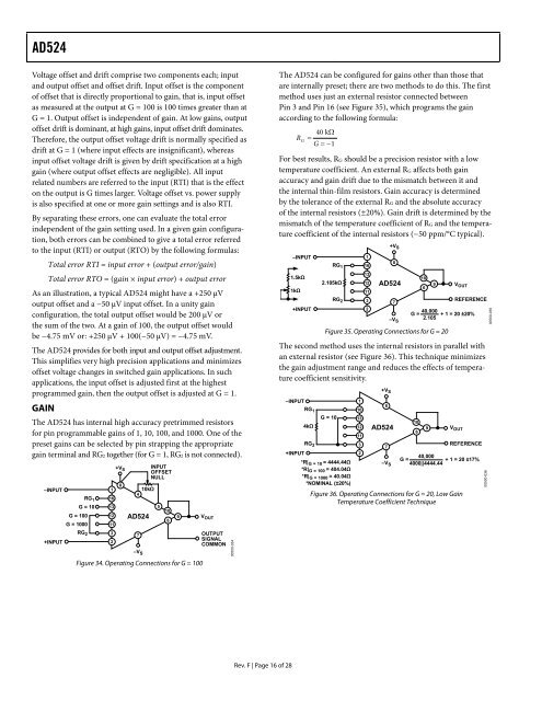
<strong>AD524</strong>Voltage offset and drift comprise two components each; inputand output offset and offset drift. Input offset is the componentof offset that is directly proportional to gain, that is, input offsetas measured at the output at G = 100 is 100 times greater than atG = 1. Output offset is independent of gain. At low gains, outputoffset drift is dominant, at high gains, input offset drift dominates.Therefore, the output offset voltage drift is normally specified asdrift at G = 1 (where input effects are insignificant), whereasinput offset voltage drift is given by drift specification at a highgain (where output offset effects are negligible). All inputrelated numbers are referred to the input (RTI) that is the effecton the output is G times larger. Voltage offset vs. power supplyis also specified at one or more gain settings and is also RTI.By separating these errors, one can evaluate the total errorindependent of the gain setting used. In a given gain configuration,both errors can be combined to give a total error referredto the input (RTI) or output (RTO) by the following formulas:Total error RTI = input error + (output error/gain)Total error RTO = (gain × input error) + output errorAs an illustration, a typical <strong>AD524</strong> might have a +250 μVoutput offset and a −50 μV input offset. In a unity gainconfiguration, the total output offset would be 200 μV orthe sum of the two. At a gain of 100, the output offset wouldbe −4.75 mV or: +250 μV + 100(−50 μV) = −4.75 mV.The <strong>AD524</strong> provides for both input and output offset adjustment.This simplifies very high precision applications and minimizesoffset voltage changes in switched gain applications. In suchapplications, the input offset is adjusted first at the highestprogrammed gain, then the output offset is adjusted at G = 1.GAINThe <strong>AD524</strong> has internal high accuracy pretrimmed resistorsfor pin programmable gains of 1, 10, 100, and 1000. One of thepreset gains can be selected by pin strapping the appropriategain terminal and RG2 together (for G = 1, RG2 is not connected).INPUTOFFSETNULL8–INPUT10kΩRG 2 374RG 1 16G = 10 13510G = 100 12 <strong>AD524</strong>96G = 100011+INPUT2Figure 34. Operating Connections for G = 100V OUTOUTPUTSIGNALCOMMON00500-034The <strong>AD524</strong> can be configured for gains other than those thatare internally preset; there are two methods to do this. The firstmethod uses just an external resistor connected betweenPin 3 and Pin 16 (see Figure 35), which programs the gainaccording to the following formula:R G40 kΩ= G = −1For best results, RG should be a precision resistor with a lowtemperature coefficient. An external RG affects both gainaccuracy and gain drift due to the mismatch between it andthe internal thin-film resistors. Gain accuracy is determinedby the tolerance of the external RG and the absolute accuracyof the internal resistors (±20%). Gain drift is determined by themismatch of the temperature coefficient of RG and the temperaturecoefficient of the internal resistors (−50 ppm/°C typical).–INPUT1.5kΩ1kΩ+INPUT1RG 1 16132.105kΩ1211RG 2 32+V S8<strong>AD524</strong>7–V S1069V OUTREFERENCE40,000G = + 1 = 20 ±20%2.105Figure 35. Operating Connections for G = 20The second method uses the internal resistors in parallel withan external resistor (see Figure 36). This technique minimizesthe gain adjustment range and reduces the effects of temperaturecoefficient sensitivity.–INPUT1RG 116G = 10 134kΩ1211RG 2 3+INPUT2*R| G = 10 = 4444.44Ω*R| G = 100 = 404.04Ω*R| G = 1000 = 40.04Ω*NOMINAL (±20%)+V S8<strong>AD524</strong>7–V S106V OUTREFERENCE40,000G =+ 1 = 20 ±17%4000||4444.44Figure 36. Operating Connections for G = 20, Low GainTemperature Coefficient Technique900500-03600500-035Rev. F | Page 16 of 28