AD524 Precision Instrumentation Amplifier Data ... - Analog Devices
AD524 Precision Instrumentation Amplifier Data ... - Analog Devices
AD524 Precision Instrumentation Amplifier Data ... - Analog Devices

Create successful ePaper yourself
Turn your PDF publications into a flip-book with our unique Google optimized e-Paper software.
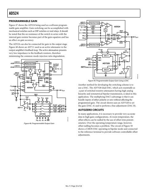
<strong>AD524</strong>PROGRAMMABLE GAINFigure 47 shows the <strong>AD524</strong> being used as a software programmablegain amplifier. Gain switching can be accomplished withmechanical switches such as DIP switches or reed relays. It shouldbe noted that the on resistance of the switch in series with theinternal gain resistor becomes part of the gain equation and hasan effect on gain accuracy.The <strong>AD524</strong> can also be connected for gain in the output stage.Figure 48 shows an AD711 used as an active attenuator in theoutput amplifier’s feedback loop. The active attenuation presentsvery low impedance to the feedback resistors, thereforeminimizing the common-mode rejection ratio degradation.–IN+IN–V S+V S1µF35V(+INPUT)(–INPUT)INPUTOFFSETNULL123410kΩ5678PROTECTION16OUTPUTOFFSETPROTECTION15 NULL+V TO –VS14 R210kΩ4.44kΩ1320kΩ20kΩ20kΩ+ –<strong>AD524</strong>20kΩ20kΩ20kΩ20kΩAD7590404Ω1240Ω10pFV SS V DD GND+V S1 8 16–152+1314AD7111112–V SV DD93 4 5 6 7A2 A3 A4 WRFigure 48. Programmable Output Gain111091039.2kΩ28.7kΩ316kΩV OUT1kΩ1kΩ1kΩ00500-048+INPUT(–INPUT)1G = 10 13G = 100 12G = 1000 11RG 1 16RG 2–INPUT(+INPUT)32DATAINPUTSCSWRDAC A/DAC BPROTECTION4.44kΩ404Ω40ΩPROTECTION414 DB071516618DB7V b20kΩ+V S17 3DAC ADAC B20kΩAD75285<strong>AD524</strong>20kΩ20kΩ21192020kΩ20kΩ10961/2AD712256:11/2AD712Figure 49. Programmable Output Gain Using a DACAnother method for developing the switching scheme is touse a DAC. The AD7528 dual DAC, which acts essentially asa pair of switched resistive attenuators having high analoglinearity and symmetrical bipolar transmission, is ideal in thisapplication. The multiplying DAC’s advantage is that it canhandle inputs of either polarity or zero without affecting theprogrammed gain. The circuit shown uses an AD7528 to setthe gain (DAC A) and to perform a fine adjustment (DAC B).V OUTAUTOZERO CIRCUITSIn many applications, it is necessary to provide very accuratedata in high gain configurations. At room temperature, theoffset effects can be nulled by the use of offset trim potentiometers.Over the operating temperature range, however,offset nulling becomes a problem. The circuit of Figure 50shows a CMOS DAC operating in bipolar mode and connectedto the reference terminal to provide software controllable offsetadjustments.00500-049Rev. F | Page 20 of 28