Data Sheet: DiskOnChip G3 64MB (512Mb)/128MB (1Gb) - FTP
Data Sheet: DiskOnChip G3 64MB (512Mb)/128MB (1Gb) - FTP
Data Sheet: DiskOnChip G3 64MB (512Mb)/128MB (1Gb) - FTP

You also want an ePaper? Increase the reach of your titles
YUMPU automatically turns print PDFs into web optimized ePapers that Google loves.
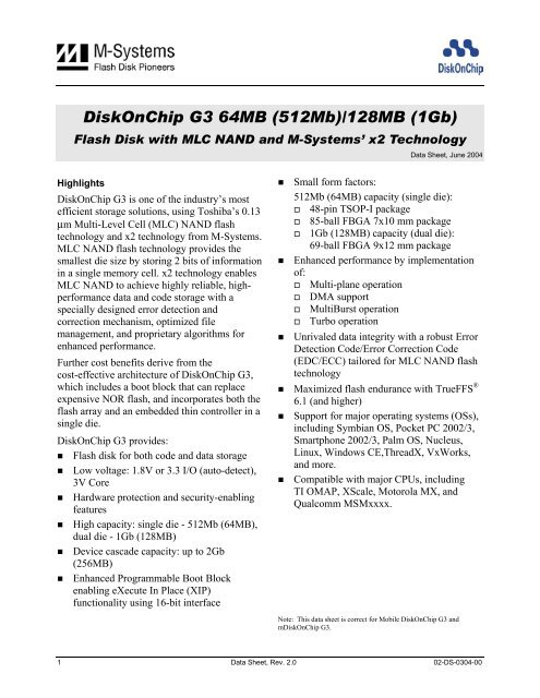
<strong>DiskOnChip</strong> <strong>G3</strong> <strong>64MB</strong> (<strong>512Mb</strong>)/<strong>128MB</strong> (<strong>1Gb</strong>)<br />
Flash Disk with MLC NAND and M-Systems’ x2 Technology<br />
<strong>Data</strong> <strong>Sheet</strong>, June 2004<br />
Highlights<br />
<strong>DiskOnChip</strong> <strong>G3</strong> is one of the industry’s most<br />
efficient storage solutions, using Toshiba’s 0.13<br />
µm Multi-Level Cell (MLC) NAND flash<br />
technology and x2 technology from M-Systems.<br />
MLC NAND flash technology provides the<br />
smallest die size by storing 2 bits of information<br />
in a single memory cell. x2 technology enables<br />
MLC NAND to achieve highly reliable, highperformance<br />
data and code storage with a<br />
specially designed error detection and<br />
correction mechanism, optimized file<br />
management, and proprietary algorithms for<br />
enhanced performance.<br />
Further cost benefits derive from the<br />
cost-effective architecture of <strong>DiskOnChip</strong> <strong>G3</strong>,<br />
which includes a boot block that can replace<br />
expensive NOR flash, and incorporates both the<br />
flash array and an embedded thin controller in a<br />
single die.<br />
<strong>DiskOnChip</strong> <strong>G3</strong> provides:<br />
• Flash disk for both code and data storage<br />
• Low voltage: 1.8V or 3.3 I/O (auto-detect),<br />
3V Core<br />
• Hardware protection and security-enabling<br />
features<br />
• High capacity: single die - <strong>512Mb</strong> (<strong>64MB</strong>),<br />
dual die - <strong>1Gb</strong> (<strong>128MB</strong>)<br />
• Device cascade capacity: up to 2Gb<br />
(256MB)<br />
• Enhanced Programmable Boot Block<br />
enabling eXecute In Place (XIP)<br />
functionality using 16-bit interface<br />
• Small form factors:<br />
<strong>512Mb</strong> (<strong>64MB</strong>) capacity (single die):<br />
48-pin TSOP-I package<br />
85-ball FBGA 7x10 mm package<br />
<strong>1Gb</strong> (<strong>128MB</strong>) capacity (dual die):<br />
69-ball FBGA 9x12 mm package<br />
• Enhanced performance by implementation<br />
of:<br />
Multi-plane operation<br />
DMA support<br />
MultiBurst operation<br />
Turbo operation<br />
• Unrivaled data integrity with a robust Error<br />
Detection Code/Error Correction Code<br />
(EDC/ECC) tailored for MLC NAND flash<br />
technology<br />
• Maximized flash endurance with TrueFFS ®<br />
6.1 (and higher)<br />
• Support for major operating systems (OSs),<br />
including Symbian OS, Pocket PC 2002/3,<br />
Smartphone 2002/3, Palm OS, Nucleus,<br />
Linux, Windows CE,ThreadX, VxWorks,<br />
and more.<br />
• Compatible with major CPUs, including<br />
TI OMAP, XScale, Motorola MX, and<br />
Qualcomm MSMxxxx.<br />
Note: This data sheet is correct for Mobile <strong>DiskOnChip</strong> <strong>G3</strong> and<br />
m<strong>DiskOnChip</strong> <strong>G3</strong>.<br />
1 <strong>Data</strong> <strong>Sheet</strong>, Rev. 2.0 02-DS-0304-00
<strong>DiskOnChip</strong> <strong>G3</strong> <strong>64MB</strong> (<strong>512Mb</strong>)/<strong>128MB</strong> (<strong>1Gb</strong>)<br />
Performance<br />
• MultiBurst read: 80 MB/sec<br />
• Erase: 30 MB/sec<br />
• Sustained read: 5 MB/sec<br />
• Sustained write: 1.1 MB/sec<br />
• Cycle Time<br />
MultiBurst: Up to 25 nsec<br />
• Access time:<br />
Normal: 55 nsec<br />
Turbo: 33 nsec<br />
Protection & Security-Enabling Features<br />
• 16-byte Unique Identification (UID)<br />
number<br />
• 6KByte user-controlled One Time<br />
Programmable (OTP) area<br />
• Two configurable hardware-protected<br />
partitions for data and code:<br />
Read-only mode<br />
Write-only mode<br />
One-Time Write mode (ROM-like)<br />
partition<br />
Protection key and LOCK# signal<br />
Sticky Lock (SLOCK) to lock boot<br />
partition<br />
Protected Bad Block Table<br />
Reliability and <strong>Data</strong> Integrity<br />
• Hardware- and software-driven, on-the-fly<br />
EDC and ECC algorithms<br />
• 4-bit Error Detection Code/Error Correction<br />
Code (EDC/ECC), based on a patented<br />
combination of BCH and Hamming code<br />
algorithms, tailored for MLC NAND flash<br />
technology<br />
• Guaranteed data integrity after power<br />
failure<br />
• Transparent bad-block management<br />
• Dynamic and static wear-leveling<br />
Boot Capability<br />
• Programmable Boot Block with XIP<br />
capability to replace boot NOR<br />
2KB for <strong>512Mb</strong> (<strong>64MB</strong>) devices<br />
4KB for <strong>1Gb</strong> (<strong>128MB</strong>) devices<br />
• Download Engine (DE) for automatic<br />
download of boot code from Programmable<br />
Boot Block<br />
• Boot options:<br />
CPU initialization<br />
Platform initialization<br />
OS boot<br />
• Asynchronous Boot mode to boot from<br />
ARM-based CPUs, e.g. XScale, TI OMAP,<br />
Motorola MX without the need for external<br />
glue logic<br />
• Exceptional boot performance with<br />
MultiBurst operation and DMA support<br />
enhanced by external clock<br />
Hardware Compatibility<br />
• Configurable interface: simple NOR-like or<br />
multiplexed address/data interface<br />
• CPU compatibility, including:<br />
ARM-based CPUs<br />
Texas Instruments OMAP<br />
Intel StrongARM/XScale<br />
Motorola MX family<br />
Emblaze ER4525<br />
Renesas SH mobile<br />
Qualcomm MSMxxxx<br />
AMD Alchemy<br />
Motorola PowerPC MPC8xx<br />
Philips PR31700<br />
Hitachi SuperH SH-x<br />
NEC VR Series<br />
• Supports 8-, 16- and 32-bit architectures<br />
Note: Refer to application note AP-DOC-0704, Improving<br />
<strong>DiskOnChip</strong> Performance, for more information about <strong>DiskOnChip</strong><br />
performance parameters.<br />
2 <strong>Data</strong> <strong>Sheet</strong>, Rev. 2.0 02-DS-0304-00
<strong>DiskOnChip</strong> <strong>G3</strong> <strong>64MB</strong> (<strong>512Mb</strong>)/<strong>128MB</strong> (<strong>1Gb</strong>)<br />
TrueFFS ® Software<br />
• Full hard-disk read/write emulation for<br />
transparent file system management<br />
• Patented TrueFFS<br />
Flash file system management<br />
Automatic block management<br />
<strong>Data</strong> management to maximize the limit<br />
of typical flash life expectancy<br />
Dynamic virtual mapping<br />
• Dynamic and static wear-leveling<br />
• Programming, duplicating, testing and<br />
debugging tools available in source code<br />
Operating Environment<br />
• Wide OS support, including:<br />
Symbian OS (EPOC)<br />
Pocket PC 2002/3<br />
Smartphone 2002/3<br />
Palm OS<br />
Nucleus<br />
Windows CE<br />
Linux<br />
ThreadX<br />
OSE<br />
VxWorks<br />
• TrueFFS Software Development Kit (SDK)<br />
for quick and easy support for proprietary<br />
OSs, or OS-less environment<br />
• TrueFFS Boot Software Development Kit<br />
(BDK)<br />
Power Requirements<br />
• Operating voltage<br />
Core: 2.5V to 3.6V<br />
I/O: 1.65 to 2.0V; or 2.5V to 3.6V<br />
(auto-detect)<br />
• Current Consumption<br />
Active mode:<br />
Read: 4.2 mA<br />
Program/erase: 7.2 mA<br />
Deep Power-Down mode:<br />
10 µA (<strong>512Mb</strong>/<strong>64MB</strong>)<br />
20 µA (<strong>1Gb</strong>/<strong>128MB</strong>)<br />
Capacity and Packaging<br />
• <strong>64MB</strong> (<strong>512Mb</strong>) capacity (single die):<br />
Device cascading option for up to four<br />
devices (2Gb)<br />
48-pin TSOP-I package:<br />
20x12x1.2 mm (width x length x height)<br />
85-ball FBGA package:<br />
7x10x1.2 mm (width x length x height)<br />
Pinout compatible with <strong>DiskOnChip</strong><br />
Plus TSOP-I products<br />
Ballout compatible with <strong>DiskOnChip</strong><br />
Plus FBGA products: 9x12 mm<br />
• <strong>128MB</strong> (<strong>1Gb</strong>) capacity (dual die):<br />
Device cascading option for up to two<br />
devices (2Gb)<br />
69-ball FBGA package:<br />
9x12x1.4 mm (width x length x height)<br />
Ballout compatible with <strong>DiskOnChip</strong><br />
Plus FBGA products:<br />
9x12 mm<br />
3 <strong>Data</strong> <strong>Sheet</strong>, Rev. 2.0 02-DS-0304-00
<strong>DiskOnChip</strong> <strong>G3</strong> <strong>64MB</strong> (<strong>512Mb</strong>)/<strong>128MB</strong> (<strong>1Gb</strong>)<br />
REVISION HISTORY<br />
Note to Mobile <strong>DiskOnChip</strong> <strong>G3</strong> customers: This data sheet is a reissue of the Mobile<br />
<strong>DiskOnChip</strong> <strong>G3</strong> data sheet (document number 91-SR-011-05-8L, Rev. 1.2), whose revision history<br />
is shown below.<br />
Doc. No Revision Date Description Reference<br />
91-SR-011-05-<br />
8L<br />
1.1 September<br />
2003<br />
Updated RSRVD signal description Section 2.2.3<br />
Section 2.3.3<br />
Section 2.4.3<br />
<strong>DiskOnChip</strong> Control<br />
Register/Control Confirmation<br />
Register mapping corrected<br />
Section 7.8<br />
Icc – Active supply current updated Section 10.2.3<br />
Mechanical dimensions for 7x10<br />
FBGA package updated<br />
69-ball FBGA 9x12 daisy-chain<br />
ordering information updated<br />
Section 10.4.1<br />
Section 11<br />
1.2 November 2003<br />
02-DS-0304-00 1.0 March 2004<br />
2.0 June 2004<br />
Update timing parameters of<br />
MultiBurst Read Cycle<br />
Added TSOP and FBGA package<br />
weight information<br />
The number of read cycles from<br />
offset 0x1FFF to move <strong>DiskOnChip</strong><br />
from Deep Power-Down mode to<br />
Normal mode was changed.<br />
The Tsu(A) for read operations was<br />
changed.<br />
Information about the Read<br />
Address Register was added<br />
Table 1<br />
Section 10.4<br />
Section 6.3<br />
Table 16<br />
Section 7.3<br />
Flash Characteristics was added. Section 10.3.6<br />
The Tprog of <strong>DiskOnChip</strong> <strong>G3</strong> was<br />
changed<br />
The Thiz(D) parameter was<br />
updated.<br />
Added note to Signal Description<br />
tables.<br />
Section 10.3.6<br />
Table 16, Table<br />
18, and Table 20<br />
Section 2.1<br />
4 <strong>Data</strong> <strong>Sheet</strong>, Rev. 2.0 02-DS-0304-00
<strong>DiskOnChip</strong> <strong>G3</strong> <strong>64MB</strong> (<strong>512Mb</strong>)/<strong>128MB</strong> (<strong>1Gb</strong>)<br />
TABLE OF CONTENTS<br />
1. Introduction ............................................................................................................................... 9<br />
2. Product Overview.................................................................................................................... 10<br />
2.1 Product Description .......................................................................................................... 10<br />
2.2 <strong>64MB</strong> (<strong>512Mb</strong>) Standard Interface ................................................................................... 11<br />
2.2.1 Pin/Ball Diagrams...............................................................................................................11<br />
2.2.2 System Interface ................................................................................................................13<br />
2.2.3 Signal Description ..............................................................................................................14<br />
2.3 <strong>128MB</strong> (<strong>1Gb</strong>) Standard Interface ..................................................................................... 18<br />
2.3.1 Ball Diagram....................................................................................................................... 18<br />
2.3.2 System Interface ................................................................................................................19<br />
2.3.3 Signal Description ..............................................................................................................20<br />
2.4 <strong>64MB</strong> (<strong>512Mb</strong>) Multiplexed Interface................................................................................ 22<br />
2.4.1 Pin/Ball Diagram................................................................................................................. 22<br />
2.4.2 System Interface ................................................................................................................24<br />
2.4.3 Signal Description ..............................................................................................................25<br />
2.5 <strong>128MB</strong> (<strong>1Gb</strong>) Multiplexed Interface.................................................................................. 29<br />
2.5.1 Ball Diagram....................................................................................................................... 29<br />
2.5.2 System Interface ................................................................................................................30<br />
2.5.3 Signal Description ..............................................................................................................31<br />
3. Theory of Operation ................................................................................................................ 33<br />
3.1 Overview........................................................................................................................... 33<br />
3.2 System Interface...............................................................................................................34<br />
3.2.1 Standard (NOR-Like) Interface........................................................................................... 34<br />
3.2.2 Multiplexed Interface .......................................................................................................... 34<br />
3.3 Configuration Interface ..................................................................................................... 34<br />
3.4 Protection and Security-Enabling Features ...................................................................... 35<br />
3.4.1 Read/Write Protection ........................................................................................................ 35<br />
3.4.2 Unique Identification (UID) Number ................................................................................... 35<br />
3.4.3 One-Time Programmable (OTP) Area ............................................................................... 35<br />
3.4.4 One-Time Write (ROM-Like) Partition ................................................................................ 36<br />
3.4.5 Sticky Lock (SLOCK).......................................................................................................... 36<br />
3.5 Programmable Boot Block with eXecute In Place (XIP) Functionality.............................. 36<br />
3.6 Download Engine (DE)..................................................................................................... 36<br />
3.7 Error Detection Code/Error Correction Code (EDC/ECC) ................................................ 37<br />
5 <strong>Data</strong> <strong>Sheet</strong>, Rev. 2.0 02-DS-0304-00
<strong>DiskOnChip</strong> <strong>G3</strong> <strong>64MB</strong> (<strong>512Mb</strong>)/<strong>128MB</strong> (<strong>1Gb</strong>)<br />
3.8 <strong>Data</strong> Pipeline .................................................................................................................... 37<br />
3.9 Control and Status............................................................................................................ 37<br />
3.10 Flash Architecture.............................................................................................................37<br />
4. x2 Technology ......................................................................................................................... 40<br />
4.1 MultiBurst Operation......................................................................................................... 40<br />
4.2 DMA Operation................................................................................................................. 42<br />
4.3 Combined MultiBurst Mode and DMA Operation ............................................................. 43<br />
4.4 Turbo Operation ............................................................................................................... 43<br />
5. Hardware Protection ............................................................................................................... 44<br />
5.1 Method of Operation......................................................................................................... 44<br />
5.2 Low-Level Structure of the Protected Area....................................................................... 45<br />
6. Modes of Operation................................................................................................................. 47<br />
6.1 Normal Mode.................................................................................................................... 48<br />
6.2 Reset Mode ......................................................................................................................48<br />
6.3 Deep Power-Down Mode ................................................................................................. 48<br />
6.4 TrueFFS Technology........................................................................................................ 49<br />
6.4.1 General Description............................................................................................................ 49<br />
6.4.2 Built-In Operating System Support..................................................................................... 50<br />
6.4.3 TrueFFS Software Development Kit (SDK)........................................................................ 50<br />
6.4.4 File Management................................................................................................................ 50<br />
6.4.5 Bad-Block Management ..................................................................................................... 50<br />
6.4.6 Wear-Leveling .................................................................................................................... 50<br />
6.4.7 Power Failure Management ............................................................................................... 51<br />
6.4.8 Error Detection/Correction.................................................................................................. 52<br />
6.4.9 Special Features Through I/O Control (IOCTL) Mechanism.............................................. 52<br />
6.4.10 Compatibility....................................................................................................................... 52<br />
6.5 8KB Memory Window....................................................................................................... 52<br />
7. Register Descriptions ............................................................................................................. 54<br />
7.1 Definition of Terms ........................................................................................................... 54<br />
7.2 Reset Values ....................................................................................................................54<br />
7.3 Read Address Register .................................................................................................... 55<br />
7.4 No Operation (NOP) Register........................................................................................... 56<br />
7.5 Chip Identification (ID) Register [0:1]................................................................................ 56<br />
7.6 Test Register .................................................................................................................... 56<br />
7.7 Endian Control Register ................................................................................................... 57<br />
6 <strong>Data</strong> <strong>Sheet</strong>, Rev. 2.0 02-DS-0304-00
<strong>DiskOnChip</strong> <strong>G3</strong> <strong>64MB</strong> (<strong>512Mb</strong>)/<strong>128MB</strong> (<strong>1Gb</strong>)<br />
7.8 <strong>DiskOnChip</strong> Control Register/Control Confirmation Register ........................................... 58<br />
7.9 Device ID Select Register................................................................................................. 59<br />
7.10 Configuration Register...................................................................................................... 59<br />
7.11 Interrupt Control Register ................................................................................................. 60<br />
7.12 Interrupt Status Register................................................................................................... 61<br />
7.13 Output Control Register.................................................................................................... 62<br />
7.14 DPD Control Register....................................................................................................... 63<br />
7.15 DMA Control Register [1:0]............................................................................................... 64<br />
7.16 MultiBurst Mode Control Register..................................................................................... 66<br />
8. Booting from <strong>DiskOnChip</strong> <strong>G3</strong>................................................................................................. 67<br />
8.1 Introduction....................................................................................................................... 67<br />
8.2 Boot Procedure in PC-Compatible Platforms ................................................................... 67<br />
8.3 Boot Replacement............................................................................................................ 68<br />
8.3.1 PC Architectures ................................................................................................................68<br />
8.3.2 Non-PC Architectures......................................................................................................... 69<br />
8.3.3 Asynchronous Boot Mode .................................................................................................. 69<br />
9. Design Considerations ...........................................................................................................70<br />
9.1 General Guidelines........................................................................................................... 70<br />
9.2 Standard NOR-Like Interface ........................................................................................... 71<br />
9.3 Multiplexed Interface ........................................................................................................ 72<br />
9.4 Connecting Control Signals.............................................................................................. 72<br />
9.4.1 Standard Interface..............................................................................................................72<br />
9.4.2 Multiplexed Interface .......................................................................................................... 73<br />
9.5 Implementing the Interrupt Mechanism ............................................................................ 74<br />
9.5.1 Hardware Configuration ..................................................................................................... 74<br />
9.5.2 Software Configuration....................................................................................................... 74<br />
9.6 Device Cascading............................................................................................................. 75<br />
9.7 Boot Replacement............................................................................................................ 76<br />
9.8 Platform-Specific Issues................................................................................................... 77<br />
9.8.1 Wait State ........................................................................................................................... 77<br />
9.8.2 Big and Little Endian Systems............................................................................................ 77<br />
9.8.3 Busy Signal......................................................................................................................... 77<br />
9.8.4 Working with 8/16/32-Bit Systems...................................................................................... 77<br />
9.9 Design Environment ......................................................................................................... 79<br />
7 <strong>Data</strong> <strong>Sheet</strong>, Rev. 2.0 02-DS-0304-00
<strong>DiskOnChip</strong> <strong>G3</strong> <strong>64MB</strong> (<strong>512Mb</strong>)/<strong>128MB</strong> (<strong>1Gb</strong>)<br />
10. Product Specifications ........................................................................................................... 80<br />
10.1 Environmental Specifications ........................................................................................... 80<br />
10.1.1 Operating Temperature ...................................................................................................... 80<br />
10.1.2 Thermal Characteristics ..................................................................................................... 80<br />
10.1.3 Humidity.............................................................................................................................. 80<br />
10.1.4 Endurance .......................................................................................................................... 80<br />
10.2 Electrical Specifications.................................................................................................... 80<br />
10.2.1 Absolute Maximum Ratings................................................................................................ 80<br />
10.2.2 Capacitance........................................................................................................................ 81<br />
10.2.3 DC Electrical Characteristics over Operating Range ......................................................... 81<br />
10.2.4 AC Operating Conditions.................................................................................................... 83<br />
10.3 Timing Specifications........................................................................................................ 84<br />
10.3.1 Read Cycle Timing Standard Interface .............................................................................. 84<br />
10.3.2 Write Cycle Timing Standard Interface .............................................................................. 86<br />
10.3.3 Read Cycle Timing Multiplexed Interface........................................................................... 87<br />
10.3.4 Write Cycle Timing Multiplexed Interface........................................................................... 88<br />
10.3.5 Read Cycle Timing MultiBurst............................................................................................ 89<br />
10.3.6 Flash Characteristics.......................................................................................................... 90<br />
10.3.7 Power Supply Sequence .................................................................................................... 90<br />
10.3.8 Power-Up Timing................................................................................................................ 90<br />
10.3.9 Interrupt Timing .................................................................................................................. 92<br />
10.3.10 DMA Request Timing ......................................................................................................... 92<br />
10.4 Mechanical Dimensions.................................................................................................... 93<br />
10.4.1 <strong>DiskOnChip</strong> <strong>G3</strong> <strong>64MB</strong> (<strong>512Mb</strong>).......................................................................................... 93<br />
10.4.2 <strong>DiskOnChip</strong> <strong>G3</strong> <strong>128MB</strong> (<strong>1Gb</strong>)............................................................................................ 95<br />
11. Ordering Information............................................................................................................... 96<br />
A. Sample Code............................................................................................................................ 97<br />
How to Contact Us ........................................................................................................................ 99<br />
8 <strong>Data</strong> <strong>Sheet</strong>, Rev. 2.0 02-DS-0304-00
<strong>DiskOnChip</strong> <strong>G3</strong> <strong>64MB</strong> (<strong>512Mb</strong>)/<strong>128MB</strong> (<strong>1Gb</strong>)<br />
1. INTRODUCTION<br />
This data sheet includes the following sections:<br />
Section 1: Overview of data sheet contents<br />
Section 2:<br />
Section 3:<br />
Section 4:<br />
Section 5:<br />
Section 6:<br />
Section 7:<br />
Section 8:<br />
Section 9:<br />
Section 10:<br />
Section 11:<br />
Product overview, including a brief product description, ball diagrams and signal<br />
descriptions<br />
Theory of operation for the major building blocks<br />
Major features and benefits of x2 technology<br />
Detailed description of hardware protection and security-enabling features<br />
Detailed description of modes of operation and TrueFFS technology, including<br />
power failure management and 8KByte memory window<br />
<strong>DiskOnChip</strong> <strong>G3</strong> register descriptions<br />
Overview of how to boot from <strong>DiskOnChip</strong> <strong>G3</strong><br />
Hardware and software design considerations<br />
Environmental, electrical, timing and product specifications<br />
Information on ordering <strong>DiskOnChip</strong> <strong>G3</strong><br />
For additional information on M-Systems’ flash disk products, please contact one of the offices<br />
listed on the back page.<br />
9 <strong>Data</strong> <strong>Sheet</strong>, Rev. 2.0 02-DS-0304-00
<strong>DiskOnChip</strong> <strong>G3</strong> <strong>64MB</strong> (<strong>512Mb</strong>)/<strong>128MB</strong> (<strong>1Gb</strong>)<br />
2. PRODUCT OVERVIEW<br />
2.1 Product Description<br />
<strong>DiskOnChip</strong> <strong>G3</strong> is the latest addition to M-Systems’ <strong>DiskOnChip</strong> product family. <strong>DiskOnChip</strong> <strong>G3</strong>,<br />
packed in the smallest available FBGA package with <strong>64MB</strong> (<strong>512Mb</strong>) capacity, is a single-die<br />
device with an embedded thin flash controller and flash memory. It uses Toshiba’s cutting-edge,<br />
0.13 µ NAND-based Multi-Level Cell (MLC) flash technology, enhanced by M-Systems’<br />
proprietary x2 technology. A dual-die device is available with single chip capacity of <strong>128MB</strong><br />
(<strong>1Gb</strong>).<br />
MLC NAND technology enables two bits of data to be stored on a single cell, cutting in half the<br />
physical die size. M-Systems’ proprietary x2 technology overcomes MLC-related error patterns and<br />
slow transfer rates by using a robust error detection and correction (EDC/ECC) mechanism.<br />
Furthermore, it provides performance enhancement with multi-plane operation, DMA support, turbo<br />
operation and MultiBurst operation. The combination of MLC and x2 technology results in a lowcost,<br />
minimal-sized flash disk that achieves unsurpassed reliability levels and enhanced<br />
performance.<br />
This breakthrough in performance, size and cost makes <strong>DiskOnChip</strong> <strong>G3</strong> the ideal solution for<br />
product manufacturers who require high-capacity, small size, high-performance, and above all,<br />
high-reliability storage to enable applications such as Digital TVs (DTVs), rugged handheld<br />
terminals, Digital Still Cameras (DSCs), Mobile Point of Sale (POS), telecom equipment,<br />
multimedia phones, camera and Video on Demand (VOD) phones, enhanced Multimedia<br />
Messaging Service (MMS), gaming, video and Personal Information Management (PIM) on mobile<br />
handsets, and Personal Digital Assistants (PDAs).<br />
As with the <strong>DiskOnChip</strong> Plus family (G2), <strong>DiskOnChip</strong> <strong>G3</strong> content protection and securityenabling<br />
features offer several benefits. Two write- and read-protected partitions, with both<br />
software- and hardware-based protection, can be configured independently for maximum design<br />
flexibility. The 16-byte Unique ID (UID) identifies each flash device, eliminating the need for a<br />
separate ID device on the motherboard. The 6KB One Time Programmable (OTP) area, written to<br />
once and then locked to prevent data and code from being altered, is ideal for storing customer and<br />
product-specific information.<br />
<strong>DiskOnChip</strong> <strong>G3</strong> <strong>64MB</strong> (<strong>512Mb</strong>) has a 2KB Programmable Boot Block (4KB for <strong>DiskOnChip</strong> <strong>G3</strong><br />
<strong>128MB</strong>/<strong>1Gb</strong>). This block provides eXecute In Place (XIP) functionality, enabling <strong>DiskOnChip</strong> <strong>G3</strong><br />
to replace the boot device and function as the only non-volatile memory device on-board.<br />
Eliminating the need for an additional boot device reduces hardware expenditures, board real estate,<br />
programming time, and logistics.<br />
M-Systems’ patented TrueFFS software technology fully emulates a hard disk to manage the files<br />
stored on <strong>DiskOnChip</strong> <strong>G3</strong>. This transparent file system management enables read/write operations<br />
that are identical to a standard, sector-based hard disk. In addition, TrueFFS employs patented<br />
methods, such as virtual mapping, dynamic and static wear-leveling, and automatic block<br />
management to ensure high data reliability and to maximize flash life expectancy.<br />
10 <strong>Data</strong> <strong>Sheet</strong>, Rev. 2.0 02-DS-0304-00
<strong>DiskOnChip</strong> <strong>G3</strong> <strong>64MB</strong> (<strong>512Mb</strong>)/<strong>128MB</strong> (<strong>1Gb</strong>)<br />
2.2 <strong>64MB</strong> (<strong>512Mb</strong>) Standard Interface<br />
2.2.1 Pin/Ball Diagrams<br />
See Figure 1 and Figure 2 for the <strong>DiskOnChip</strong> <strong>G3</strong> <strong>64MB</strong> (<strong>512Mb</strong>) pinout/ballout for the standard<br />
interface. To ensure proper device functionality, pins/balls marked RSRVD are reserved for future<br />
use and should not be connected.<br />
Note: Third-generation <strong>DiskOnChip</strong> <strong>G3</strong> is designed as a drop-in replacement for second-generation<br />
(G2) <strong>DiskOnChip</strong> Plus products, assuming that the latter were integrated according to<br />
migration guide guidelines. Refer to the <strong>DiskOnChip</strong> Plus (G2) to <strong>DiskOnChip</strong> <strong>G3</strong>/P3<br />
migration guide for further information.<br />
TSOP-I Package<br />
RSTIN#<br />
CE#<br />
WE#<br />
OE#<br />
A12<br />
A11<br />
A10<br />
A9<br />
A8<br />
A7<br />
A6<br />
VCC<br />
VSS<br />
A5<br />
A4<br />
A3<br />
A2<br />
A1<br />
A0/DPD<br />
RSRVD<br />
DMARQ#<br />
IF_CFG<br />
LOCK#<br />
ID0<br />
1<br />
2<br />
3<br />
4<br />
5<br />
6<br />
7<br />
8<br />
9<br />
10<br />
11<br />
12<br />
13<br />
14<br />
15<br />
16<br />
17<br />
18<br />
19<br />
20<br />
21<br />
22<br />
23<br />
24<br />
<strong>DiskOnChip</strong> <strong>G3</strong> <strong>64MB</strong><br />
48-Pin TSOP-I<br />
48 VSS<br />
47 IRQ#<br />
46 D15<br />
45 D14<br />
44 D13<br />
43 D12<br />
42 D11<br />
41 D10<br />
40 D9<br />
39 D8<br />
38 CLK<br />
37 VCCQ<br />
36 VSS<br />
35 D7<br />
34 D6<br />
33 D5<br />
32 D4<br />
31 D3<br />
30 D2<br />
D1<br />
29<br />
28<br />
27<br />
26<br />
25<br />
D0<br />
BUSY#<br />
ID1<br />
VSS<br />
Figure 1: TSOP-I Pinout for Standard Interface (<strong>DiskOnChip</strong> <strong>G3</strong> <strong>64MB</strong>/<strong>512Mb</strong>)<br />
11 <strong>Data</strong> <strong>Sheet</strong>, Rev. 2.0 02-DS-0304-00
<strong>DiskOnChip</strong> <strong>G3</strong> <strong>64MB</strong> (<strong>512Mb</strong>)/<strong>128MB</strong> (<strong>1Gb</strong>)<br />
7x10 FBGA Package<br />
1 2 3 4 5 6 7 8<br />
A<br />
M<br />
M<br />
M<br />
M<br />
B<br />
M M<br />
M M M M M M<br />
C<br />
A A7 RSRVD RSRVD WE# A8 A11<br />
D<br />
A3 A6 RSRVD RSTIN# RSRVD RSRVD A12 RSRVD<br />
E<br />
A2 A5 RSRVD BUSY# RSRVD A9 LOCK# RSRVD<br />
F<br />
A1 A4 IF_CFG M M A10 ID0 IRQ#<br />
G<br />
A0/<br />
DPD<br />
VSS<br />
D1 M M D6 DMARQ# ID1<br />
H<br />
CE# OE#<br />
D9 D3 D4 D13 D15 RSRVD<br />
J<br />
RSRVD D0<br />
D10 VCC VCCQ D12 D7 VSS<br />
K<br />
D8 D2 D11 CLK D5 D14<br />
L<br />
M M<br />
M M M M M M<br />
M<br />
M M<br />
M M<br />
Figure 2: 7x10 FBGA Ballout for Standard Interface (<strong>DiskOnChip</strong> <strong>G3</strong> <strong>64MB</strong>/<strong>512Mb</strong>)<br />
12 <strong>Data</strong> <strong>Sheet</strong>, Rev. 2.0 02-DS-0304-00
<strong>DiskOnChip</strong> <strong>G3</strong> <strong>64MB</strong> (<strong>512Mb</strong>)/<strong>128MB</strong> (<strong>1Gb</strong>)<br />
2.2.2 System Interface<br />
See Figure 3 for a simplified I/O diagram for a standard interface of <strong>DiskOnChip</strong> <strong>G3</strong> <strong>64MB</strong><br />
(<strong>512Mb</strong>).<br />
CE#, OE#, WE#<br />
BUSY#<br />
A[12:0]<br />
D]15:0]<br />
<strong>DiskOnChip</strong> <strong>G3</strong><br />
RSTIN#<br />
CLK<br />
DMARQ#<br />
IRQ#<br />
DPD<br />
ID[1:0] IF_CFG LOCK#<br />
System Interface<br />
Configuration<br />
Control<br />
Figure 3: Standard Interface Simplified I/O Diagram (<strong>DiskOnChip</strong> <strong>G3</strong> <strong>64MB</strong>/<strong>512Mb</strong>)<br />
13 <strong>Data</strong> <strong>Sheet</strong>, Rev. 2.0 02-DS-0304-00
<strong>DiskOnChip</strong> <strong>G3</strong> <strong>64MB</strong> (<strong>512Mb</strong>)/<strong>128MB</strong> (<strong>1Gb</strong>)<br />
2.2.3 Signal Description<br />
<strong>DiskOnChip</strong> <strong>G3</strong> TSOP-I and FBGA packages support identical signals. The related pin and ball<br />
designations are listed in the signal descriptions, presented in logic groups, in Table 2 and Table 3.<br />
TSOP-I Package<br />
Table 2: Signal Descriptions for Standard Interface (<strong>DiskOnChip</strong> <strong>64MB</strong>/<strong>512Mb</strong> TSOP-I Package)<br />
Signal<br />
A[12:6]<br />
A[5:0]<br />
Pin No.<br />
5-11<br />
14-19<br />
Input<br />
Type 1,2 Description Signal Type<br />
System Interface<br />
ST Address bus. A0 is multiplexed with the DPD pin. Input<br />
D[15:8] 46-39 ST, R8 <strong>Data</strong> bus, high byte. Not used and may be left<br />
floating when IF_CFG is set to 0 (8-bit mode).<br />
Input/<br />
Output<br />
D[7:0] 35-28 ST <strong>Data</strong> bus, low byte. Input/<br />
Output<br />
CE# 2 ST Chip Enable, active low Input<br />
WE# 3 ST Write Enable, active low Input<br />
OE# 4 ST Output Enable, active low Input<br />
Configuration<br />
ID[1:0] 26, 24 ST Identification. Configuration control to support up to<br />
four chips cascaded in the same memory window.<br />
Chip 1 = ID1, ID0 = VSS, VSS (0,0); must be used<br />
for single-chip configuration<br />
Chip 2 = ID1, ID0 = VSS, VCCQ (0,1)<br />
Chip 3 = ID1, ID0 = VCCQ, VSS (1,0)<br />
Chip 4 = ID1, ID0 = VCCQ, VCCQ (1,1)<br />
Input<br />
LOCK# 23 ST Lock, active low. When active, provides full<br />
hardware data protection of selected partitions.<br />
IF_CFG 22 ST Interface Configuration, 1(VCCQ) for 16-bit interface<br />
mode, 0 (VSS) for 8-bit interface mode.<br />
Control<br />
BUSY# 27 OD Busy, active low, open drain. Indicates that<br />
Output<br />
<strong>DiskOnChip</strong> is initializing and should not be<br />
accessed. A 10 KΩ pull-up resistor is required if this<br />
pin drives an input. A 10 KΩ pull-up resistor is<br />
recommended even if this pin is not used.<br />
RSTIN# 1 ST Reset, active low. Input<br />
CLK 38 ST System Clock. Input<br />
DMARQ# 21 OD DMA Request, active low. A 10 KΩ pull-up resistor is<br />
required if this pin drives an input. A 10 KΩ pull-up<br />
resistor is recommended even if this pin is not used.<br />
Output<br />
Input<br />
Input<br />
14 <strong>Data</strong> <strong>Sheet</strong>, Rev. 2.0 02-DS-0304-00
<strong>DiskOnChip</strong> <strong>G3</strong> <strong>64MB</strong> (<strong>512Mb</strong>)/<strong>128MB</strong> (<strong>1Gb</strong>)<br />
Signal<br />
Pin No.<br />
Input<br />
Type 1,2 Description Signal Type<br />
IRQ# 47 OD Interrupt Request, active low. A 10 KΩ pull-up<br />
resistor is required if this pin drives an input. A<br />
10 KΩ pull-up resistor is recommended even if this<br />
pin is not used.<br />
DPD 19 ST Deep Power-Down. Used to enter and exit Deep<br />
Power-Down mode. This pin is assigned A0 instead<br />
of DPD when working in 8-bit mode.<br />
Output<br />
Input<br />
Power<br />
VCC 12 - Device core power supply. Requires a 10 nF and 0.1<br />
µF capacitor.<br />
VCCQ 37 - I/O power supply. Sets the logic 1 voltage level<br />
range of I/O pins. VCCQ may be either 2.5V to 3.6V<br />
or 1.65V to 2.0V. Requires a 10 nF and 0.1 µF<br />
capacitor.<br />
Supply<br />
Supply<br />
VSS 13, 25, 36, 48 - Ground. All VSS pins must be connected. Supply<br />
Other<br />
RSRVD 20 - Reserved. If compatibility with previous <strong>DiskOnChip</strong><br />
versions is necessary:<br />
In 16-bit mode (IF_CFG = 1) this pin must be<br />
connected to GND for compatibility with G2 devices.<br />
In 8-bit mode (IF_CFG = 0) may be left floating.<br />
Refer to the <strong>DiskOnChip</strong> Plus (G2) to <strong>DiskOnChip</strong><br />
<strong>G3</strong>/P3 migration guide for design guidelines when<br />
migrating from previous <strong>DiskOnChip</strong> versions (G2).<br />
1. The following abbreviations are used: IN - Standard (non-Schmidt) input, ST - Schmidt Trigger input, OD - Open drain output, R8 -<br />
Nominal 22K pull-up resistor, enabled only for 8-bit interface mode (IF_CFG input is 0)<br />
2. Input buffers are Schmidt trigger type only for VCCQ>2.5V.<br />
15 <strong>Data</strong> <strong>Sheet</strong>, Rev. 2.0 02-DS-0304-00
<strong>DiskOnChip</strong> <strong>G3</strong> <strong>64MB</strong> (<strong>512Mb</strong>)/<strong>128MB</strong> (<strong>1Gb</strong>)<br />
7x10 FBGA Package<br />
Table 3: Signal Descriptions for Standard Interface (<strong>DiskOnChip</strong> <strong>64MB</strong>/<strong>512Mb</strong> <strong>G3</strong> 7x10 FBGA Package)<br />
Signal<br />
A[12:11]<br />
A[10:8]<br />
A[7:4]<br />
A[3:0]<br />
D[15:14]<br />
D[13:12]<br />
D[11:8]<br />
D[7:6]<br />
D[5:3]<br />
D[2:0]<br />
Ball No.<br />
D7, C7<br />
F6, E6, C6<br />
C2, D2, E2, F2<br />
D1, E1, F1, G1<br />
H7, K7<br />
H6, J6<br />
K4, J3, H3, K2<br />
J7, G6<br />
K6, H5, H4<br />
K3, <strong>G3</strong>, J2<br />
Input<br />
Type 1,2 Description Signal Type<br />
System Interface<br />
ST Address bus. A0 is multiplexed with the DPD ball. Input<br />
ST, R8 <strong>Data</strong> bus, high byte. Not used and may be left<br />
floating when IF_CFG is set to 0 (8-bit mode).<br />
Input/<br />
Output<br />
ST <strong>Data</strong> bus, low byte. Input/<br />
Output<br />
CE# H1 ST Chip Enable, active low Input<br />
OE# H2 ST Output Enable, active low Input<br />
WE# C5 ST Write Enable, active low Input<br />
Configuration<br />
ID[1:0] G8, F7 ST Identification. Configuration control to support up to<br />
four chips cascaded in the same memory window.<br />
Chip 1 = ID1, ID0 = VSS, VSS (0,0); must be used<br />
for single chip configuration<br />
Chip 2 = ID1, ID0 = VSS, VCCQ (0,1)<br />
Chip 3 = ID1, ID0 = VCCQ, VSS (1,0)<br />
Chip 4 = ID1, ID0 = VCCQ, VCCQ (1,1)<br />
Input<br />
LOCK# E7 ST Lock, active low. When active, provides full<br />
hardware data protection of selected partitions.<br />
IF_CFG F3 ST Interface Configuration, 1 (VCCQ) for 16-bit<br />
interface mode, 0 (VSS) for 8-bit interface mode.<br />
Control<br />
BUSY# E4 OD Busy, active low, open drain. Indicates that<br />
<strong>DiskOnChip</strong> is initializing and should not be<br />
accessed. A 10 KΩ pull-up resistor is required if this<br />
ball drives an input. A 10 KΩ pull-up resistor is<br />
recommended even if this ball is not used.<br />
Input<br />
Input<br />
Output<br />
RSTIN# D4 ST Reset, active low. Input<br />
CLK K5 ST System Clock. Input<br />
DMARQ# G7 OD DMA Request, active low. A 10 KΩ pull-up resistor is<br />
required if this ball drives an input. A 10 KΩ pull-up<br />
resistor is recommended even if this ball is not used.<br />
Output<br />
16 <strong>Data</strong> <strong>Sheet</strong>, Rev. 2.0 02-DS-0304-00
<strong>DiskOnChip</strong> <strong>G3</strong> <strong>64MB</strong> (<strong>512Mb</strong>)/<strong>128MB</strong> (<strong>1Gb</strong>)<br />
Signal<br />
Ball No.<br />
Input<br />
Type 1,2 Description Signal Type<br />
IRQ# F8 OD Interrupt Request, active low. A 10 KΩ pull-up<br />
resistor is required if this ball drives an input. A 10<br />
KΩ pull-up resistor is recommended even if this ball<br />
is not used.<br />
DPD G1 ST Deep Power-Down. Used to enter and exit Deep<br />
Power-Down mode. This ball is assigned A0 instead<br />
of DPD when working in 8-bit mode.<br />
Power<br />
VCC J4 - Device supply. Requires a 10 nF and 0.1 µF<br />
capacitor.<br />
VCCQ J5 - I/O power supply. Sets the logic 1 voltage level<br />
range of I/O balls. VCCQ may be either 2.5V to 3.6V<br />
or 1.65V to 2.0V. Requires a 10 nF and<br />
0.1 µF capacitor.<br />
Output<br />
Input<br />
Supply<br />
Supply<br />
VSS G2, J8 - Ground. All VSS balls must be connected. Supply<br />
RSRVD<br />
Other<br />
E3 - Reserved. If compatibility with previous <strong>DiskOnChip</strong><br />
versions is necessary:<br />
In 16-bit mode (IF_CFG = 1) this ball must be<br />
connected to GND for compatibility with G2 devices.<br />
In 8-bit mode (IF_CFG = 0) may be left floating.<br />
Refer to the <strong>DiskOnChip</strong> Plus (G2) to <strong>DiskOnChip</strong><br />
<strong>G3</strong>/P3 migration guide for design guidelines when<br />
migrating from previous <strong>DiskOnChip</strong> versions (G2).<br />
See Figure 2 - Reserved. Other reserved signals are not connected<br />
internally and must be left floating to guarantee<br />
forward compatibility with future products.<br />
M - Mechanical. These balls are for mechanical<br />
placement, and are not connected internally.<br />
A - Alignment. This ball is for device alignment and is<br />
not connected internally.<br />
1. The following abbreviations are used: IN - Standard (non-Schmidt) input, ST - Schmidt Trigger input, OD - Open drain output, R8 -<br />
Nominal 22K pull-up resistor, enabled only for 8-bit interface mode (IF_CFG input is 0)<br />
2. Input buffers are Schmidt trigger type only for VCCQ>2.5V.<br />
17 <strong>Data</strong> <strong>Sheet</strong>, Rev. 2.0 02-DS-0304-00
<strong>DiskOnChip</strong> <strong>G3</strong> <strong>64MB</strong> (<strong>512Mb</strong>)/<strong>128MB</strong> (<strong>1Gb</strong>)<br />
2.3 <strong>128MB</strong> (<strong>1Gb</strong>) Standard Interface<br />
2.3.1 Ball Diagram<br />
See Figure 4 for the <strong>DiskOnChip</strong> <strong>G3</strong> <strong>128MB</strong> (<strong>1Gb</strong>) standard interface ballout. To ensure proper<br />
device functionality, balls marked RSRVD are reserved for future use and should not be connected.<br />
Note: <strong>DiskOnChip</strong> <strong>G3</strong> <strong>1Gb</strong>(<strong>128MB</strong>) is designed as a drop-in replacement for <strong>DiskOnChip</strong> <strong>G3</strong><br />
<strong>64MB</strong> (<strong>512Mb</strong>), assuming that the board was designed according to migration guide<br />
guidelines. Refer to the <strong>DiskOnChip</strong> Plus (G2) to <strong>DiskOnChip</strong> <strong>G3</strong>/P3 migration guide for<br />
further information.<br />
9x12 FBGA Package<br />
1 2 3 4 5 6 7 8 9 10<br />
A<br />
M<br />
M<br />
B<br />
M<br />
M<br />
C<br />
A<br />
A7<br />
RSRVD<br />
RSRVD<br />
WE#<br />
A8<br />
A11<br />
D<br />
A3<br />
A6<br />
RSRVD<br />
RSTIN#<br />
RSRVD<br />
RSRVD<br />
A12<br />
RSRVD<br />
E<br />
A2<br />
A5<br />
RSRVD<br />
BUSY#<br />
RSRVD<br />
A9<br />
LOCK#<br />
RSRVD<br />
F<br />
M<br />
A1<br />
A4<br />
IF_CFG<br />
A10<br />
ID0<br />
IRQ#<br />
M<br />
G<br />
M<br />
A0/<br />
DPD<br />
VSS<br />
D1<br />
D6<br />
DMARQ#<br />
ID1<br />
M<br />
H<br />
CE#<br />
OE#<br />
D9<br />
D3<br />
D4<br />
D13<br />
D15<br />
RSRVD<br />
J<br />
RSRVD<br />
D0<br />
D10<br />
VCC VCCQ D12<br />
D7<br />
VSS<br />
K<br />
D8<br />
D2<br />
D11<br />
CLK<br />
D5<br />
D14<br />
L<br />
M<br />
M<br />
M<br />
M<br />
M<br />
Figure 4 Ballout for Standard Interface (<strong>DiskOnChip</strong> <strong>G3</strong> <strong>128MB</strong>/<strong>1Gb</strong> 9x12 FBGA Package)<br />
18 <strong>Data</strong> <strong>Sheet</strong>, Rev. 2.0 02-DS-0304-00
<strong>DiskOnChip</strong> <strong>G3</strong> <strong>64MB</strong> (<strong>512Mb</strong>)/<strong>128MB</strong> (<strong>1Gb</strong>)<br />
2.3.2 System Interface<br />
See Figure 5 for a simplified I/O diagram for a standard interface of <strong>DiskOnChip</strong> <strong>G3</strong> <strong>128MB</strong> (<strong>1Gb</strong>).<br />
CE#, OE#, WE#<br />
BUSY#<br />
A[12:0]<br />
D]15:0]<br />
<strong>DiskOnChip</strong> <strong>G3</strong><br />
RSTIN#<br />
CLK<br />
DMARQ#<br />
IRQ#<br />
DPD<br />
ID[1:0] IF_CFG LOCK#<br />
System Interface<br />
Configuration<br />
Control<br />
Figure 5: Standard Interface Simplified I/O Diagram (<strong>DiskOnChip</strong> <strong>G3</strong> <strong>128MB</strong>/<strong>1Gb</strong>)<br />
19 <strong>Data</strong> <strong>Sheet</strong>, Rev. 2.0 02-DS-0304-00
<strong>DiskOnChip</strong> <strong>G3</strong> <strong>64MB</strong> (<strong>512Mb</strong>)/<strong>128MB</strong> (<strong>1Gb</strong>)<br />
2.3.3 Signal Description<br />
9x12 FBGA Package<br />
Table 4: Signal Descriptions for Standard Interface (<strong>DiskOnChip</strong> <strong>G3</strong> <strong>128MB</strong>/<strong>1Gb</strong> 9x12 FBGA Package)<br />
Signal<br />
A[12:11]<br />
A[10:8]<br />
A[7:4]<br />
A[3:0]<br />
D[15:14]<br />
D[13:12]<br />
D[11:8]<br />
D[7:6]<br />
D[5:3]<br />
D[2:0]<br />
Ball No.<br />
D8, C8<br />
F7, E7, C7<br />
C3, D3, E3, F3<br />
D2, E2, F2, G2<br />
H8, K8<br />
H7, J7<br />
K5, J4, H4, K3<br />
J8, G7<br />
K7, H6, H5<br />
K4, G4, J3<br />
Input<br />
Type 1,2 Description Signal Type<br />
System Interface<br />
ST Address bus. A0 is multiplexed with the DPD ball. Input<br />
ST, R8 <strong>Data</strong> bus, high byte. Not used and may be left<br />
floating when IF_CFG is set to 0 (8-bit mode).<br />
Input/<br />
Output<br />
ST <strong>Data</strong> bus, low byte. Input/<br />
Output<br />
CE# H2 ST Chip Enable, active low. Input<br />
OE# H3 ST Output Enable, active low. Input<br />
WE# C6 ST Write Enable, active low. Input<br />
Configuration<br />
ID[1:0] G9, F8 ST Identification. Configuration control to support up to<br />
two chips cascaded in the same memory window.<br />
Chip 1 = ID1, ID0 = VSS, VSS (0,0); must be used<br />
for single chip configuration<br />
Chip 2 = ID1, ID0 = VCCQ, VCCQ (1,1)<br />
Input<br />
LOCK# E8 ST Lock, active low. When active, provides full<br />
hardware data protection of selected partitions.<br />
IF_CFG F4 ST Interface Configuration, 1 (VCCQ) for 16-bit<br />
interface mode, 0 (VSS) for 8-bit interface mode.<br />
Control<br />
BUSY# E5 OD Busy, active low, open drain. Indicates that<br />
<strong>DiskOnChip</strong> is initializing and should not be<br />
accessed. A 10 KΩ pull-up resistor is required if this<br />
ball drives an input. A 10 KΩ pull-up resistor is<br />
recommended even if this ball is not used.<br />
Input<br />
Input<br />
Output<br />
RSTIN# D5 ST Reset, active low. Input<br />
CLK K6 ST System Clock. Input<br />
DMARQ# G8 OD DMA Request, active low. A 10 KΩ pull-up resistor is<br />
required if this ball drives an input. A 10 KΩ pull-up<br />
resistor is recommended even if this ball is not used.<br />
Output<br />
20 <strong>Data</strong> <strong>Sheet</strong>, Rev. 2.0 02-DS-0304-00
<strong>DiskOnChip</strong> <strong>G3</strong> <strong>64MB</strong> (<strong>512Mb</strong>)/<strong>128MB</strong> (<strong>1Gb</strong>)<br />
Signal<br />
Ball No.<br />
Input<br />
Type 1,2 Description Signal Type<br />
IRQ# F9 OD Interrupt Request, active low. A 10 KΩ pull-up<br />
resistor is required if this ball drives an input. A 10<br />
KΩ pull-up resistor is recommended even if this ball<br />
is not used.<br />
DPD G2 ST Deep Power-Down. Used to enter and exit Deep<br />
Power-Down mode. Pin is assigned A0 instead of<br />
DPD when working in 8-bit mode.<br />
Power<br />
VCC J5 - Device supply. Requires a 10 nF and 0.1 µF<br />
capacitor.<br />
VCCQ J6 - I/O power supply. Sets the logic 1 voltage level<br />
range of I/O balls. VCCQ may be either 2.5V to 3.6V<br />
or 1.65V to 2.0V. Requires a 10 nF and 0.1 µF<br />
capacitor.<br />
Output<br />
Input<br />
Supply<br />
Supply<br />
VSS <strong>G3</strong>, J9 - Ground. All VSS balls must be connected. Supply<br />
RSRVD<br />
Other<br />
E4 - Reserved. If compatibility with previous <strong>DiskOnChip</strong><br />
versions is necessary:<br />
In 16-bit mode (IF_CFG = 1) this ball must be<br />
connected to GND for compatibility with G2 devices.<br />
In 8-bit mode (IF_CFG = 0) may be left floating.<br />
Refer to the <strong>DiskOnChip</strong> Plus (G2) to <strong>DiskOnChip</strong><br />
<strong>G3</strong>/P3 migration guide for design guidelines when<br />
migrating from previous <strong>DiskOnChip</strong> versions (G2).<br />
See Figure 4 - Reserved. Other reserved signals are not connected<br />
internally and must be left floating to guarantee<br />
forward compatibility with future products.<br />
M<br />
Mechanical. These balls are for mechanical<br />
placement, and are not connected internally.<br />
A - Alignment. This ball is for device alignment and is<br />
not connected internally.<br />
1. The following abbreviations are used: IN - Standard (non-Schmidt) input, ST - Schmidt Trigger input, OD - Open drain output, R8 -<br />
Nominal 22K pull-up resistor, enabled only for 8-bit interface mode (IF_CFG input is 0)<br />
2. Input buffers are Schmidt trigger type only for VCCQ>2.5V.<br />
21 <strong>Data</strong> <strong>Sheet</strong>, Rev. 2.0 02-DS-0304-00
<strong>DiskOnChip</strong> <strong>G3</strong> <strong>64MB</strong> (<strong>512Mb</strong>)/<strong>128MB</strong> (<strong>1Gb</strong>)<br />
2.4 <strong>64MB</strong> (<strong>512Mb</strong>) Multiplexed Interface<br />
2.4.1 Pin/Ball Diagram<br />
See Figure 6 and Figure 7 for the <strong>DiskOnChip</strong> <strong>G3</strong> <strong>64MB</strong> (<strong>512Mb</strong>) pinout/ballout for the<br />
multiplexed interface. To ensure proper device functionality, pins/balls marked RSRVD are<br />
reserved for future use and should not be connected.<br />
Note: Third-generation <strong>DiskOnChip</strong> <strong>G3</strong> is designed as a drop-in replacement for second-generation<br />
(G2) <strong>DiskOnChip</strong> Plus products, assuming that the latter were integrated according to<br />
migration guide guidelines. Refer to the <strong>DiskOnChip</strong> Plus (G2) to <strong>DiskOnChip</strong> <strong>G3</strong>/P3<br />
migration guide for further information.<br />
TSOP-I Package<br />
RSTIN#<br />
CE#<br />
WE#<br />
OE#<br />
VSS<br />
VSS<br />
VSS<br />
VSS<br />
VSS<br />
VSS<br />
VSS<br />
VSS<br />
VSS<br />
VSS<br />
VSS<br />
VSS<br />
VSS<br />
VSS<br />
DPD<br />
NC<br />
DMARQ#<br />
VCCQ<br />
LOCK#<br />
ID0<br />
1<br />
2<br />
3<br />
4<br />
5<br />
6<br />
7<br />
8<br />
9<br />
10<br />
11<br />
12<br />
13<br />
14<br />
15<br />
16<br />
17<br />
18<br />
19<br />
20<br />
21<br />
22<br />
23<br />
24<br />
<strong>DiskOnChip</strong> <strong>G3</strong> <strong>64MB</strong><br />
48-Pin TSOP-I<br />
48 VSS<br />
47 IRQ#<br />
46 AD15<br />
45 AD14<br />
44 AD13<br />
43 AD12<br />
42 AD11<br />
41 AD10<br />
40 AD9<br />
39 AD8<br />
38 CLK<br />
37 VCCQ<br />
36 GND<br />
35 AD7<br />
34 AD6<br />
33 AD5<br />
32 AD4<br />
31 AD3<br />
30 AD2<br />
AD1<br />
29<br />
28<br />
27<br />
26<br />
25<br />
AD0<br />
BUSY#<br />
AVD#<br />
VSS<br />
Figure 6: Pinout for Multiplexed Interface (<strong>DiskOnChip</strong> <strong>64MB</strong>/<strong>512Mb</strong> TSOP-I Package)<br />
22 <strong>Data</strong> <strong>Sheet</strong>, Rev. 2.0 02-DS-0304-00
<strong>DiskOnChip</strong> <strong>G3</strong> <strong>64MB</strong> (<strong>512Mb</strong>)/<strong>128MB</strong> (<strong>1Gb</strong>)<br />
7x10 FBGA Package<br />
1 2 3 4 5 6 7 8<br />
A<br />
M<br />
M<br />
M<br />
M<br />
B<br />
M M<br />
M M M M M M<br />
C<br />
A VSS RSRVD RSRVD WE# VSS VSS<br />
D<br />
VSS VSS RSRVD RSTIN# RSRVD RSRVD VSS RSRVD<br />
E<br />
VSS VSS RSRVD BUSY# RSRVD VSS LOCK# RSRVD<br />
F<br />
VSS VSS VCCQ M M VSS ID0 IRQ#<br />
G<br />
DPD VSS<br />
AD1 M M AD6 DMARQ# AVD#<br />
H<br />
CE# OE#<br />
AD9 AD3 AD4 AD13 AD15 RSRVD<br />
J<br />
RSRVD AD0<br />
AD10 VCC VCCQ AD12 AD7 VSS<br />
K<br />
AD8 AD2 AD11 CLK AD5 AD14<br />
L<br />
M M<br />
M M M M M M<br />
M<br />
M M<br />
M M<br />
Figure 7 Ballout for Multiplexed Interface (<strong>DiskOnChip</strong> <strong>64MB</strong>/<strong>512Mb</strong> 7x10 FBGA Package)<br />
23 <strong>Data</strong> <strong>Sheet</strong>, Rev. 2.0 02-DS-0304-00
<strong>DiskOnChip</strong> <strong>G3</strong> <strong>64MB</strong> (<strong>512Mb</strong>)/<strong>128MB</strong> (<strong>1Gb</strong>)<br />
2.4.2 System Interface<br />
See Figure 8 for a simplified I/O diagram of <strong>DiskOnChip</strong> <strong>G3</strong> <strong>64MB</strong> (<strong>512Mb</strong>).<br />
BUSY#<br />
CE#, OC#, WE#<br />
AD[15:0]<br />
<strong>DiskOnChip</strong> <strong>G3</strong><br />
RSTIN#<br />
CLK<br />
DMARQ#<br />
IRQ#<br />
DPD<br />
ID0 AVD# LOCK#<br />
System Interface<br />
Configuration<br />
Control<br />
Figure 8: Multiplexed Interface Simplified I/O Diagram (<strong>DiskOnChip</strong> <strong>G3</strong> <strong>64MB</strong>/<strong>512Mb</strong> 7x10 FBGA Package)<br />
24 <strong>Data</strong> <strong>Sheet</strong>, Rev. 2.0 02-DS-0304-00
<strong>DiskOnChip</strong> <strong>G3</strong> <strong>64MB</strong> (<strong>512Mb</strong>)/<strong>128MB</strong> (<strong>1Gb</strong>)<br />
2.4.3 Signal Description<br />
<strong>DiskOnChip</strong> <strong>G3</strong> <strong>64MB</strong> (<strong>512Mb</strong>) TSOP-I and 7x10 FBGA packages support identical signals in the<br />
multiplexed interface. The related pin/ball designations are listed in the signal descriptions,<br />
presented in logic groups, in Table 5 and Table 6.<br />
TSOP-I Package<br />
Table 5: Signal Descriptions for Multiplexed Interface (<strong>DiskOnChip</strong> <strong>G3</strong> <strong>64MB</strong>/<strong>512Mb</strong> TSOP-I Package)<br />
Signal<br />
Pin No.<br />
Input<br />
Type 1,2<br />
Description<br />
Signal<br />
Type<br />
System Interface<br />
AD[15:0] 28-35, 39-46 ST Multiplexed bus. Address and data signals. Input/<br />
Output<br />
CE# 2 ST Chip Enable, active low. Input<br />
WE# 3 ST Write Enable, active low. Input<br />
OE# 4 ST Output Enable, active low. Input<br />
Configuration<br />
AVD# 26 ST Set multiplexed interface. Input<br />
ID0 24 ST Identification. Configuration control to support up to two chips<br />
cascaded in the same memory window.<br />
Chip 1 = ID0 = VSS; must be used for single-chip<br />
configuration<br />
Chip 2 = ID0 = VCCQ<br />
Input<br />
LOCK# 23 ST Lock, active low. When active, provides full hardware data<br />
protection of selected partitions.<br />
Control<br />
BUSY# 27 OD Busy, active low, open drain. Indicates that <strong>DiskOnChip</strong> is<br />
initializing and should not be accessed.<br />
A 10 KΩ pull-up resistor is required if this pin drives an input.<br />
A 10 KΩ pull-up resistor is recommended even if this pin is<br />
not used.<br />
Input<br />
Output<br />
RSTIN# 1 ST Reset, active low. Input<br />
CLK 38 ST System Clock. Input<br />
DMARQ# 21 OD DMA Request, active low. A 10 KΩ pull-up resistor is required<br />
if this pin drives an input. A 10 KΩ pull-up resistor is<br />
recommended even if this pin is not used.<br />
IRQ# 47 OD Interrupt Request, active low. A 10 KΩ pull-up resistor is<br />
required if this pin drives an input. A 10 KΩ pull-up resistor is<br />
recommended even if this pin is not used.<br />
DPD 19 ST Deep Power-Down. Used to enter and exit Deep Power-<br />
Down mode. Multiplexed with A0 when working in 16-bit<br />
mode.<br />
Output<br />
Input<br />
25 <strong>Data</strong> <strong>Sheet</strong>, Rev. 2.0 02-DS-0304-00
<strong>DiskOnChip</strong> <strong>G3</strong> <strong>64MB</strong> (<strong>512Mb</strong>)/<strong>128MB</strong> (<strong>1Gb</strong>)<br />
Signal Pin No.<br />
Input<br />
Type 1,2<br />
Description<br />
Power<br />
VCCQ 37,22 - I/O power supply. Sets the logic 1 voltage level range of I/O<br />
pins. VCCQ may be either 2.5V to 3.6V or 1.65V to 2.0V.<br />
Requires a 10 nF and 0.1 µF capacitor.<br />
Signal<br />
Type<br />
Supply<br />
VCC 12 - Device core supply. Requires a 10 nF and 0.1 µF capacitor. Supply<br />
VSS 5-11, 14-18,<br />
13, 25, 36, 48<br />
- Ground. All VSS pins must be connected. Supply<br />
Reserved<br />
RSRVD 20 - Reserved signal that is not connected internally and must be<br />
left floating to guarantee forward compatibility with future<br />
products. It should not be connected to arbitrary signals.<br />
1. The following abbreviations are used: IN - Standard (non-Schmidt) input, ST - Schmidt Trigger input, OD - Open drain output<br />
2. Input buffers are Schmidt trigger type only for VCCQ>2.5V.<br />
26 <strong>Data</strong> <strong>Sheet</strong>, Rev. 2.0 02-DS-0304-00
<strong>DiskOnChip</strong> <strong>G3</strong> <strong>64MB</strong> (<strong>512Mb</strong>)/<strong>128MB</strong> (<strong>1Gb</strong>)<br />
7x10 FBGA Package<br />
Table 6: Signal Descriptions for Multiplexed Interface (<strong>DiskOnChip</strong> <strong>G3</strong> <strong>64MB</strong>/<strong>512Mb</strong> 7x10 FBGA Package)<br />
Signal<br />
AD[15:14]<br />
AD[13:12]<br />
AD[11:9]<br />
AD[8:6]<br />
AD[5:3]<br />
AD[2:0]<br />
Pin No.<br />
H7, K7<br />
H6, J6<br />
K4, J3, H3<br />
K2, J7, G6<br />
K6, H5, H4<br />
K3, <strong>G3</strong>, J2<br />
Input<br />
Type 1,2<br />
System Interface<br />
Description<br />
Signal<br />
Type<br />
ST Multiplexed bus. Address and data signals Input/<br />
Output<br />
CE# H1 ST Chip Enable, active low Input<br />
OE# H2 ST Write Enable, active low Input<br />
WE# C5 ST Output Enable, active low Input<br />
Configuration<br />
AVD# G8 ST Set multiplexed interface Input<br />
ID0 F7 ST Identification. Configuration control to support up to two chips Input<br />
cascaded in the same memory window.<br />
Chip 1 = ID0 = VSS; must be used for single-chip<br />
configuration<br />
Chip 2 = ID0 = VCC<br />
LOCK# E7 ST Lock, active low. When active, provides full hardware data<br />
protection of selected partitions.<br />
Control<br />
BUSY# E4 OD Busy, active low, open drain. Indicates that <strong>DiskOnChip</strong> is<br />
initializing and should not be accessed A 10 KΩ pull-up<br />
resistor is required if this ball drives an input. A 10 KΩ pull-up<br />
resistor is recommended even if this ball is not used.<br />
RSTIN# D4 ST Reset, active low. Input<br />
CLK K5 ST System Clock. Input<br />
DMARQ# G7 OD DMA Request, active low. A 10 KΩ pull-up resistor is required<br />
if this ball drives an input. A 10 KΩ pull-up resistor is<br />
recommended even if this ball is not used.<br />
IRQ# F8 OD Interrupt Request, active low. A 10 KΩ pull-up resistor is<br />
required if this ball drives an input. A 10 KΩ pull-up resistor is<br />
recommended even if this ball is not used.<br />
DPD G1 ST Deep Power-Down. Used to enter and exit Deep Power-<br />
Down mode. Pin is assigned A0 instead of DPD when<br />
working in 8-bit mode.<br />
Input<br />
Output<br />
Output<br />
Output<br />
Input<br />
27 <strong>Data</strong> <strong>Sheet</strong>, Rev. 2.0 02-DS-0304-00
<strong>DiskOnChip</strong> <strong>G3</strong> <strong>64MB</strong> (<strong>512Mb</strong>)/<strong>128MB</strong> (<strong>1Gb</strong>)<br />
Signal<br />
Pin No.<br />
Input<br />
Type 1,2<br />
Description<br />
Signal<br />
Type<br />
Power<br />
VCC J4 - Device core supply. Requires a 10 nF and 0.1 µF capacitor. Supply<br />
VCCQ J5, F3 - I/O power supply. Sets the logic 1 voltage level range of I/O<br />
balls. VCCQ may be either 2.5V to 3.6V or 1.65V to 2.0V.<br />
Requires a 10 nF and 0.1 µF capacitor.<br />
VSS G2,J8, D7,<br />
C7, F6, E6,<br />
C6, C2, D2,<br />
E2, F2, D1,<br />
E1, F1<br />
Supply<br />
- Ground. All VSS pins must be connected. Supply<br />
Other<br />
Reserved See Figure 7 - Reserved. Reserved signals are not connected internally and<br />
must be left floating to guarantee forward compatibility with<br />
future products.<br />
M<br />
Mechanical. These balls are for mechanical placement, and<br />
are not connected internally.<br />
A - Alignment. This ball is for device alignment and is not<br />
connected internally.<br />
1. The following abbreviations are used: IN - Standard (non-Schmidt) input, ST - Schmidt Trigger input, OD - Open drain output<br />
2. Input buffers are Schmidt trigger type only for VCCQ>2.5V.<br />
28 <strong>Data</strong> <strong>Sheet</strong>, Rev. 2.0 02-DS-0304-00
<strong>DiskOnChip</strong> <strong>G3</strong> <strong>64MB</strong> (<strong>512Mb</strong>)/<strong>128MB</strong> (<strong>1Gb</strong>)<br />
2.5 <strong>128MB</strong> (<strong>1Gb</strong>) Multiplexed Interface<br />
2.5.1 Ball Diagram<br />
See Figure 9 for the <strong>DiskOnChip</strong> <strong>G3</strong> <strong>128MB</strong> (<strong>1Gb</strong>) ball diagram. To ensure proper device<br />
functionality, balls marked RSRVD are reserved for future use and should not be connected.<br />
Note: <strong>DiskOnChip</strong> <strong>G3</strong> <strong>1Gb</strong>(<strong>128MB</strong>) is designed as a drop-in replacement for <strong>DiskOnChip</strong> G2<br />
<strong>64MB</strong>/<strong>512Mb</strong>, assuming that the board was designed according to the migration guide<br />
guidelines. Refer to the <strong>DiskOnChip</strong> Plus (G2) to <strong>DiskOnChip</strong> <strong>G3</strong>/P3 migration guide for<br />
further information.<br />
9x12 FBGA Package<br />
1 2 3 4 5 6 7 8 9 10<br />
A<br />
M<br />
M<br />
B<br />
M<br />
M<br />
C<br />
A<br />
VSS<br />
RSRVD<br />
RSRVD<br />
WE#<br />
VSS<br />
VSS<br />
D<br />
VSS<br />
VSS<br />
RSRVD<br />
RSTIN#<br />
RSRVD<br />
RSRVD<br />
VSS<br />
RSRVD<br />
E<br />
VSS<br />
VSS<br />
RSRVD<br />
BUSY#<br />
RSRVD<br />
VSS<br />
LOCK#<br />
RSRVD<br />
F<br />
M<br />
VSS<br />
VSS<br />
VCCQ<br />
VSS<br />
ID0(VSS)<br />
IRQ#<br />
M<br />
G<br />
M<br />
DPD<br />
VSS<br />
AD1<br />
AD6<br />
DMARQ#<br />
AVD#<br />
M<br />
H<br />
CE#<br />
OE#<br />
AD9<br />
AD3<br />
AD4<br />
AD13<br />
AD15<br />
RSRVD<br />
J<br />
RSRVD<br />
AD0<br />
AD10<br />
VCC VCCQ AD12 AD7<br />
VSS<br />
K<br />
AD8<br />
AD2<br />
AD11<br />
CLK<br />
AD5<br />
AD14<br />
L<br />
M<br />
M<br />
M<br />
M<br />
M<br />
Figure 9: Ballout for Multiplexed Interface (<strong>DiskOnChip</strong> <strong>G3</strong> <strong>128MB</strong>/<strong>1Gb</strong> 9x12 FBGA Package)<br />
29 <strong>Data</strong> <strong>Sheet</strong>, Rev. 2.0 02-DS-0304-00
<strong>DiskOnChip</strong> <strong>G3</strong> <strong>64MB</strong> (<strong>512Mb</strong>)/<strong>128MB</strong> (<strong>1Gb</strong>)<br />
2.5.2 System Interface<br />
See Figure 10 for a simplified I/O diagram of <strong>DiskOnChip</strong> <strong>G3</strong> <strong>128MB</strong> (<strong>1Gb</strong>).<br />
BUSY#<br />
CE#, OC#, WE#<br />
AD[15:0]<br />
<strong>DiskOnChip</strong> <strong>G3</strong><br />
RSTIN#<br />
CLK<br />
DMARQ#<br />
IRQ#<br />
DPD<br />
ID0 AVD# LOCK#<br />
System Interface<br />
Configuration<br />
Control<br />
Figure 10: Multiplexed Interface Simplified I/O Diagram (<strong>DiskOnChip</strong> <strong>G3</strong> <strong>128MB</strong>/<strong>1Gb</strong> 9x12 FBGA Package)<br />
30 <strong>Data</strong> <strong>Sheet</strong>, Rev. 2.0 02-DS-0304-00
<strong>DiskOnChip</strong> <strong>G3</strong> <strong>64MB</strong> (<strong>512Mb</strong>)/<strong>128MB</strong> (<strong>1Gb</strong>)<br />
2.5.3 Signal Description<br />
9x12 FBGA Package<br />
Table 7: Signal Descriptions for Multiplexed Interface (<strong>DiskOnChip</strong> <strong>G3</strong> <strong>128MB</strong>/<strong>1Gb</strong> 9x12 FBGA Package)<br />
Signal<br />
Ball No.<br />
Input<br />
Type 1,2<br />
Description<br />
Signal<br />
Type<br />
AD[15:14]<br />
AD[13:12]<br />
AD[11:9]<br />
AD[8:6]<br />
AD[5:3]<br />
AD[2:0]<br />
H8, K8<br />
H7, J7<br />
K5, J4, H4<br />
K3, J8, G7<br />
K7, H6, H5<br />
K4, G4, J3<br />
System Interface<br />
ST Multiplexed bus. Address and data signals Input/<br />
Output<br />
CE# H2 ST Chip Enable, active low Input<br />
OE# H3 ST Write Enable, active low Input<br />
WE# C6 ST Output Enable, active low Input<br />
Configuration<br />
AVD# G9 ST Set multiplexed interface Input<br />
ID0 F8 ST Identification. NC for <strong>DiskOnChip</strong> <strong>G3</strong> <strong>128MB</strong> (<strong>1Gb</strong>). Input<br />
LOCK# E8 ST Lock, active low. When active, provides full hardware data<br />
protection of selected partitions.<br />
Control<br />
BUSY# E5 OD Busy, active low, open drain. Indicates that <strong>DiskOnChip</strong> is<br />
initializing and should not be accessed. A 10 KΩ pull-up<br />
resistor is required if this pin/ball drives an input. A 10 KΩ pullup<br />
resistor is recommended even if this pin/ball is not used.<br />
Input<br />
Output<br />
RSTIN# D5 ST Reset, active low. Input<br />
CLK K6 ST System Clock. Input<br />
DMARQ# G8 OD DMA Request, active low. A 10 KΩ pull-up resistor is required<br />
if this pin/ball drives an input. A 10 KΩ pull-up resistor is<br />
recommended even if this pin/ball is not used.<br />
IRQ# F9 OD Interrupt Request, active low. A 10 KΩ pull-up resistor is<br />
required if this pin/ball drives an input. A 10 KΩ pull-up resistor<br />
is recommended even if this pin/ball is not used.<br />
DPD G2 ST Deep Power-Down. Used to enter and exit Deep Power-Down<br />
mode. Multiplexed with A0 when working in 16-bit mode.<br />
Output<br />
Output<br />
Input<br />
31 <strong>Data</strong> <strong>Sheet</strong>, Rev. 2.0 02-DS-0304-00
<strong>DiskOnChip</strong> <strong>G3</strong> <strong>64MB</strong> (<strong>512Mb</strong>)/<strong>128MB</strong> (<strong>1Gb</strong>)<br />
Signal<br />
Ball No.<br />
Input<br />
Type 1,2<br />
Description<br />
Signal<br />
Type<br />
Power<br />
VCC J5 - Device core supply. Requires a 10 nF and 0.1 µF capacitor. Supply<br />
VCCQ J6, F4 - I/O power supply. Sets the logic ‘1’ voltage level range of I/O<br />
balls/pins. VCCQ may be either 2.5V to 3.6V or 1.65V to 2.0V.<br />
Requires a 10 nF and 0.1 µF capacitor.<br />
VSS <strong>G3</strong>, J9, D8,<br />
C8, F7, E7,<br />
C7, C3, D3,<br />
E3, F3, D2,<br />
E2, F2<br />
Supply<br />
- Ground. All VSS pins must be connected. Supply<br />
Other<br />
RSRVD See Figure 9 - Reserved. All reserved signals are not connected internally<br />
and must be left floating to guarantee forward compatibility<br />
with future products.<br />
M<br />
Mechanical. These balls are for mechanical placement, and<br />
are not connected internally.<br />
A - Alignment. This ball is for device alignment and is not<br />
connected internally.<br />
1. The following abbreviations are used: IN - Standard (non-Schmidt) input, ST - Schmidt Trigger input, OD - Open drain output, R8 -<br />
Nominal 22K pull-up resistor, enabled only for 8-bit interface mode (IF_CFG input is 0)<br />
2. Input buffers are Schmidt trigger type only for VCCQ>2.5V.<br />
32 <strong>Data</strong> <strong>Sheet</strong>, Rev. 2.0 02-DS-0304-00
<strong>DiskOnChip</strong> <strong>G3</strong> <strong>64MB</strong> (<strong>512Mb</strong>)/<strong>128MB</strong> (<strong>1Gb</strong>)<br />
3. THEORY OF OPERATION<br />
3.1 Overview<br />
<strong>DiskOnChip</strong> <strong>G3</strong> consists of the following major functional blocks, as shown in Figure 11.<br />
*ADDR[0] and DPD are multiplexed on the same ball/pin.<br />
Figure 11: <strong>DiskOnChip</strong> <strong>G3</strong> Simplified Block Diagram, Standard Interface<br />
These components are described briefly below and in more detail in the following sections.<br />
• System Interface for the host interface.<br />
• Configuration Interface for configuring <strong>DiskOnChip</strong> <strong>G3</strong> to operate in 8-bit, 16-bit mode,<br />
cascaded configuration, hardware read/write protection and entering/exiting Deep Power-Down<br />
mode.<br />
• Read/Write Protection and OTP for advanced data/code security and protection.<br />
• Programmable Boot Block with XIP functionality enhanced with a Download Engine (DE)<br />
for system initialization capability.<br />
• Error Detection and Error Correction Code (EDC/ECC) for on-the-fly error handling.<br />
• <strong>Data</strong> Pipeline through which the data flows from the system to the NAND flash arrays.<br />
• Control & Status block that contains registers responsible for transferring the address, data<br />
and control information between the TrueFFS driver and the flash media.<br />
• Flash Interface that interfaces to two NAND flash planes.<br />
• Bus Control for translating the host bus address, and data and control signals into valid NAND<br />
flash signals.<br />
• Address Decoder to enable the relevant unit inside the <strong>DiskOnChip</strong> controller, according to<br />
the address range received from the system interface.<br />
33 <strong>Data</strong> <strong>Sheet</strong>, Rev. 2.0 02-DS-0304-00
<strong>DiskOnChip</strong> <strong>G3</strong> <strong>64MB</strong> (<strong>512Mb</strong>)/<strong>128MB</strong> (<strong>1Gb</strong>)<br />
3.2 System Interface<br />
3.2.1 Standard (NOR-Like) Interface<br />
The system interface block provides an easy-to-integrate NOR-like (also SRAM and EEPROMlike)<br />
interface to <strong>DiskOnChip</strong> <strong>G3</strong>, enabling it to interface with various CPU interfaces, such as a<br />
local bus, ISA bus, NOR interface, SRAM interface, EEPROM interface or any other compatible<br />
interface. In addition, the EEPROM-like interface enables direct access to the Programmable Boot<br />
Block to permit XIP (Execute-In-Place) functionality during system initialization.<br />
A 13-bit wide address bus enables access to the <strong>DiskOnChip</strong> <strong>G3</strong> 8KB memory window (as shown<br />
in Section 6.5). A 32-bit internal data bus is supported by parallel access to two 32MB (256Mb)<br />
flash planes (for <strong>64MB</strong>/<strong>512Mb</strong> single-die devices), each of which enables 16-bit access. This 16-bit<br />
data bus permits 16-bit wide access to the host.<br />
The Chip Enable (CE#), Write Enable (WE#) and Output Enable (OE#) signals trigger read and<br />
write cycles. A write cycle occurs while both the CE# and the WE# inputs are asserted. Similarly, a<br />
read cycle occurs while both the CE# and OE# inputs are asserted. Note that <strong>DiskOnChip</strong> <strong>G3</strong> does<br />
not require a clock signal. It features a unique analog static design, optimized for minimal power<br />
consumption. The CE#, WE# and OE# signals trigger the controller (e.g., system interface block,<br />
bus control and data pipeline) and flash access.<br />
The Reset In (RSTIN#) and Busy (BUSY#) control signals are used in the reset phase.<br />
The Interrupt Request (IRQ#) signal can be used when long I/O operations, such as Block Erase,<br />
delay the CPU resources. The signal is also asserted when a <strong>Data</strong> Protection violation has occurred.<br />
This signal frees the CPU to run other tasks, continuing read/write operations with <strong>DiskOnChip</strong> <strong>G3</strong><br />
only after the IRQ# signal has been asserted and an interrupt handling routine (implemented in the<br />
OS) has been called to return control to the TrueFFS driver.<br />
The DMARQ# output is used to control multi-page DMA operations, and the CLK input is used to<br />
support MultiBurst operation when reading flash data. See Section 4.1 for further information.<br />
3.2.2 Multiplexed Interface<br />
In this configuration, the address and data signals are multiplexed. The ID[1] input is driven by the<br />
host AVD# signal, and the D[15:0] pins/balls, used for both address inputs and data, are connected<br />
to the host AD[15:0] bus. While AVD# is asserted, the host drives AD[11:0] with bits [12:1] of the<br />
address. Host signals AD[15:12] are not significant during this part of the cycle.<br />
This interface is automatically used when a falling edge is detected on ID[1]. This edge must occur<br />
after RSTIN# is negated and before the first read or write cycle to the controller. When using a<br />
multiplexed interface, the value of ID[1] is internally forced to logic-0. The only possible device ID<br />
values are 0 and 1; therefore, only up to two <strong>DiskOnChip</strong> <strong>G3</strong> <strong>64MB</strong> (<strong>512Mb</strong>) devices may be<br />
cascaded in multiplexed configuration (dual-die <strong>DiskOnChip</strong> <strong>G3</strong> <strong>128MB</strong> (<strong>1Gb</strong>) cannot be cascaded<br />
when used in a multiplexed interface).<br />
3.3 Configuration Interface<br />
The Configuration Interface block enables the designer to configure <strong>DiskOnChip</strong> <strong>G3</strong> to operate in<br />
different modes. The ID[1:0] signals are used in a cascaded configuration (refer to Section 9.6), the<br />
34 <strong>Data</strong> <strong>Sheet</strong>, Rev. 2.0 02-DS-0304-00
<strong>DiskOnChip</strong> <strong>G3</strong> <strong>64MB</strong> (<strong>512Mb</strong>)/<strong>128MB</strong> (<strong>1Gb</strong>)<br />
DPD signal is used to enter and exit Deep Power-Down mode (see Section 6.3), the LOCK# signal<br />
is used for hardware write/read protection, and the IF_CFG signal is used to configure 8/16-bit<br />
access.<br />
3.4 Protection and Security-Enabling Features<br />
The Protection and Security-Enabling block, consisting of read/write protection, UID and an OTP<br />
area, enables advanced data and code security and content protection. Located on the main route of<br />
traffic between the host and the flash, this block monitors and controls all data and code transactions<br />
to and from <strong>DiskOnChip</strong> <strong>G3</strong>.<br />
3.4.1 Read/Write Protection<br />
<strong>Data</strong> and code protection is implemented through a Protection State Machine (PSM). The user can<br />
configure one or two independently programmable areas of the flash memory as read protected,<br />
write protected, or read/write protected.<br />
A protected partition may be protected by either/both of these hardware mechanisms:<br />
• 64-bit protection key<br />
• Hard-wired LOCK# signal<br />
If the Lock option is enabled (by means of software) and the LOCK# signal is asserted, the<br />
protected partition has an additional hardware lock that prevents read/write access to the partition,<br />
even with the use of the correct protection key.<br />
The size and protection attributes of the protected partition are defined during the media-formatting<br />
stage.<br />
In the event of an attempt to bypass the protection mechanism, illegally modify the protection key<br />
or in any way sabotage the configuration parameters, the entire <strong>DiskOnChip</strong> <strong>G3</strong> becomes both read<br />
and write protected, and is completely inaccessible.<br />
For further information on hardware protection, please refer to the TrueFFS Software Development<br />
Kit (SDK) developer guide.<br />
3.4.2 Unique Identification (UID) Number<br />
Each <strong>DiskOnChip</strong> <strong>G3</strong> is assigned a 16-byte UID number. Burned onto the flash during production,<br />
the UID cannot be altered and is unique worldwide. The UID is essential in security-related<br />
applications, and can be used to identify end-user products in order to fight fraudulent duplication<br />
by imitators.<br />
3.4.3 One-Time Programmable (OTP) Area<br />
The 6KB OTP area is user programmable for complete customization. The user can write to this<br />
area once, after which it is automatically and permanently locked. After it is locked, the OTP area<br />
becomes read only, just like a ROM device.<br />
Typically, the OTP area is used to store customer and product information such as: product ID,<br />
software version, production data, customer ID and tracking information.<br />
35 <strong>Data</strong> <strong>Sheet</strong>, Rev. 2.0 02-DS-0304-00
<strong>DiskOnChip</strong> <strong>G3</strong> <strong>64MB</strong> (<strong>512Mb</strong>)/<strong>128MB</strong> (<strong>1Gb</strong>)<br />
3.4.4 One-Time Write (ROM-Like) Partition<br />
A partition in the <strong>DiskOnChip</strong> <strong>G3</strong> can be set as One-Time Write. After it is locked, this partition<br />
becomes read only, just like a ROM device. Its capacity is defined during the media-formatting<br />
stage.<br />
3.4.5 Sticky Lock (SLOCK)<br />
The boot partition can be locked automatically by hardware after the boot phase is completed and<br />
the device is in Normal mode. This is done by setting the Sticky Lock (SLOCK) bit in the Output<br />
Control register to 1. This has the same effect as asserting the LOCK# signal. Once set, SLOCK can<br />
only be cleared by asserting the RSTIN# input. Like the LOCK# input, assertion of this bit prevents<br />
the protection key from disabling the protection for a given partition. There is no need to mount the<br />
partition before calling a hardware protection routine.<br />
This feature can be useful when the boot code in the boot partition must be read/write protected.<br />
Upon power-up, the boot code must be unprotected so the CPU can boot directly from <strong>DiskOnChip</strong>.<br />
At the end of the boot process, protection can be set until the next power-up or reset.<br />
3.5 Programmable Boot Block with eXecute In Place (XIP) Functionality<br />
The Programmable Boot Block with XIP functionality enables <strong>DiskOnChip</strong> <strong>G3</strong> to act as a boot<br />
device in addition to performing flash disk data storage functions. This eliminates the need for<br />
expensive, legacy NOR flash or any other boot device on the motherboard.<br />
The Programmable Boot Block on <strong>DiskOnChip</strong> <strong>G3</strong> <strong>64MB</strong> (<strong>512Mb</strong>) is 2KB in size (4KB for<br />
dual-die <strong>128MB</strong>/<strong>1Gb</strong> devices). The Download Engine (DE), described in the next section, expands<br />
the functionality of this block by copying the boot code from the flash into the boot block.<br />
<strong>DiskOnChip</strong> <strong>G3</strong> <strong>64MB</strong> (<strong>512Mb</strong>) devices may be cascaded in order to form a larger flash disk.<br />
When <strong>DiskOnChip</strong> <strong>G3</strong> <strong>512Mb</strong> (<strong>64MB</strong>) is connected with a standard NOR-like interface, up to four<br />
devices may be cascaded to create a 2Gb flash disk. When <strong>DiskOnChip</strong> <strong>G3</strong> <strong>64MB</strong> (<strong>512Mb</strong>) is<br />
connected with a multiplexed interface, up to two devices may be cascaded to create a <strong>128MB</strong><br />
(<strong>1Gb</strong>) flash disk.<br />
Notes: 1. When more than one <strong>DiskOnChip</strong> <strong>G3</strong> <strong>64MB</strong> (<strong>512Mb</strong>) device is cascaded, a maximum<br />
boot block of 4KB is available. The Programmable Boot Block of each device is mapped<br />
to a unique address space.<br />
2. The Programmable Boot Block size available for <strong>DiskOnChip</strong> <strong>G3</strong> <strong>128MB</strong> (<strong>1Gb</strong>) is 4<br />
KB.<br />
3.6 Download Engine (DE)<br />
Upon power-up or when the RSTIN# signal is asserted, the DE automatically downloads the Initial<br />
Program Loader (IPL) to the Programmable Boot Block. The IPL is responsible for starting the<br />
booting process. The download process is quick, and is designed so that when the CPU accesses<br />
<strong>DiskOnChip</strong> <strong>G3</strong> for code execution, the IPL code is already located in the Programmable Boot<br />
Block. During the download process, <strong>DiskOnChip</strong> <strong>G3</strong> does not respond to read or write accesses.<br />
Host systems must therefore observe the requirements described in Section 10.3.8.<br />
36 <strong>Data</strong> <strong>Sheet</strong>, Rev. 2.0 02-DS-0304-00
<strong>DiskOnChip</strong> <strong>G3</strong> <strong>64MB</strong> (<strong>512Mb</strong>)/<strong>128MB</strong> (<strong>1Gb</strong>)<br />
In addition, the DE downloads the data protection rules from the flash to the Protection State<br />
Machines (PSM), so that <strong>DiskOnChip</strong> <strong>G3</strong> is secure and protected from the first moment it is active.<br />
During the download process, <strong>DiskOnChip</strong> <strong>G3</strong> asserts the BUSY# signal to indicate to the system<br />
that it is not yet ready to be accessed. Once BUSY# is negated, the system can access<br />
<strong>DiskOnChip</strong> <strong>G3</strong>.<br />
A failsafe mechanism prevents improper initialization due to a faulty VCC or invalid assertion of<br />
the RSTIN# input. Another failsafe mechanism is designed to overcome possible NAND flash data<br />
errors. It prevents internal registers from powering up in a state that bypasses the intended data<br />
protection. In addition, any attempt to sabotage the data structures causes the entire <strong>DiskOnChip</strong> to<br />
become both read and write protected, and completely inaccessible.<br />
3.7 Error Detection Code/Error Correction Code (EDC/ECC)<br />
Because NAND-based MLC flash is prone to errors, it requires unique error-handling capability. M-<br />
Systems’ x2 technology implements 4-bit Error Detection Code/Error Correction Code (EDC/ECC),<br />
based on a patented combination of Bose, Chaudhuri and Hocquenghem (BCH) and Hamming code<br />
algorithms. Error Detection Code (EDC) is implemented in hardware to optimize performance,<br />
while Error Correction Code (ECC) is performed in software, when required, to save silicon costs.<br />
Each time a 512-byte page is written, additional parity bits are calculated and written to the flash.<br />
Each time data is read from the flash, the parity bits are read and used to calculate error locations.<br />
The Hamming code can detect 2 errors per page and correct 1 error per page. The BCH code can<br />
detect and correct 4 errors per page. It can even detect 5 errors per page with a probability of 99.9%.<br />
It ensures that the minimal amount of code required is used for detection and correction to deliver<br />
the required reliability without degrading performance.<br />
3.8 <strong>Data</strong> Pipeline<br />
<strong>DiskOnChip</strong> <strong>G3</strong> uses a two-stage pipeline mechanism, designed for maximum performance while<br />
enabling on-the-fly data manipulation, such as read/write protection and Error Detection/Error<br />
Correction. Refer to technical note TN-DOC-014, Pipeline Mechanism in <strong>DiskOnChip</strong>, for further<br />
information.<br />
3.9 Control and Status<br />
The Control and Status block contains registers responsible for transferring address, data and<br />
control information between the <strong>DiskOnChip</strong> TrueFFS driver and the flash media. Additional<br />
registers are used to monitor the status of the flash media (ready/busy) and the <strong>DiskOnChip</strong><br />
controller. For further information on the <strong>DiskOnChip</strong> registers, refer to Section 7.<br />
3.10 Flash Architecture<br />
<strong>DiskOnChip</strong> <strong>G3</strong> <strong>64MB</strong> (<strong>512Mb</strong>) consists of two 32MB (256Mb) flash planes that consist of 1024<br />
blocks each, organized in 64 pages, as follows:<br />
• Page – Each page contains 512 bytes of user data and a 16-byte extra area that is used to store<br />
flash management and EDC/ECC signature data, as shown in Figure 12.<br />
37 <strong>Data</strong> <strong>Sheet</strong>, Rev. 2.0 02-DS-0304-00
<strong>DiskOnChip</strong> <strong>G3</strong> <strong>64MB</strong> (<strong>512Mb</strong>)/<strong>128MB</strong> (<strong>1Gb</strong>)<br />
• Block (Erase Unit) – Each block contains 64 pages (total of 256Kb), as shown in Figure 13. A<br />
block is the minimal unit that can be erased, and is sometimes referred to as an erase block.<br />
Note: Since the device works with multiple planes, the operational block size is 512Kb, as<br />
described in the next section.<br />
User <strong>Data</strong><br />
Flash Management &<br />
ECC/EDC Signature<br />
512 Bytes<br />
16 Bytes<br />
0.5 KB<br />
Figure 12: Page Structure<br />
512 Bytes<br />
16 Bytes<br />
Page 0<br />
Page 1<br />
256 Kb<br />
Page 62<br />
Page 63<br />
Figure 13: Block Structure<br />
Parallel Multi-Plane Access<br />
The two 32MB (256Mb) flash planes operate in parallel, thereby providing a true 32-bit internal<br />
data bus and four times the read, write and erase performance. Two pages on different planes can be<br />
concurrently read or written if they have the same offset within their respective units, even if the<br />
units are unaligned.<br />
Bad units are mapped individually on each plane by enabling unaligned unit access, as shown in<br />
Figure 14. Good units can therefore be aligned or unaligned, minimizing the effects of bad units on<br />
the media. Without this capability, a bad unit in one plane would cause a good unit in the second<br />
plane to be tagged as a bad unit, making it unusable. This customized method of bad unit handling<br />
for two planes enhances data utilization without adversely affecting performance.<br />
38 <strong>Data</strong> <strong>Sheet</strong>, Rev. 2.0 02-DS-0304-00
<strong>DiskOnChip</strong> <strong>G3</strong> <strong>64MB</strong> (<strong>512Mb</strong>)/<strong>128MB</strong> (<strong>1Gb</strong>)<br />
Internal Bus<br />
16-bit <strong>Data</strong> Bus<br />
16-bit <strong>Data</strong> Bus<br />
Good Unit<br />
Good Unit<br />
Good Unit<br />
Aligned Unit<br />
Aligned Unit<br />
Aligned Unit<br />
Good Unit<br />
Good Unit<br />
Good Unit<br />
Bad Unit<br />
Unaligned<br />
Unit<br />
Good Unit<br />
~ ~ ~ ~<br />
Good Unit<br />
Good Unit<br />
Good Unit<br />
Flash Plane 1<br />
Aligned Unit<br />
Aligned Unit<br />
Bad Unit<br />
Good Unit<br />
Good Unit<br />
Flash Plane 2<br />
Figure 14: Unaligned Multi-Plane Access<br />
39 <strong>Data</strong> <strong>Sheet</strong>, Rev. 2.0 02-DS-0304-00
<strong>DiskOnChip</strong> <strong>G3</strong> <strong>64MB</strong> (<strong>512Mb</strong>)/<strong>128MB</strong> (<strong>1Gb</strong>)<br />
4. X2 TECHNOLOGY<br />
<strong>DiskOnChip</strong> <strong>G3</strong> enhances performance using various proprietary techniques:<br />
• Parallel access to the separate 32MB (256Mb) flash planes, thereby providing an internal 32-bit<br />
data bus. See Section 3.10 for further information.<br />
• MultiBurst operation to read large chunks of data, providing a MultiBurst read speed of up to<br />
80 MB/sec.<br />
• DMA operation to release the CPU for other tasks in coordination with the platform’s DMA<br />
controller. This is especially useful during the boot stage. Up to 64KB of data can be<br />
transferred during a DMA operation.<br />
• Turbo operation to enhance read access time from 55 ns to 33 ns (standard interface, access to<br />
flash addresses).<br />
4.1 MultiBurst Operation<br />
MultiBurst operation is especially effective for large file reads that are typical during boot-up.<br />
During MultiBurst operation, data is read from the two flash planes in parallel through a 32-bit wide<br />
internal flash interface. <strong>Data</strong> is read by the host one 16-bit word after another using the CLK input,<br />
resulting in a MultiBurst read mode of up to 80 MB/sec. MultiBurst operation can only be<br />
performed on hosts that support burst reads. See Figure 15 below.<br />
Note: A 25 nsec cycle time during MultiBurst can be achieved at Vcc = Vccq = 2.7 ~ 3.6V).<br />
16-bit to<br />
Host<br />
WORD 0<br />
FIFO<br />
WORD 1<br />
32-bit <strong>Data</strong> Mux<br />
16-bit <strong>Data</strong><br />
16-bit <strong>Data</strong><br />
W<br />
O<br />
R<br />
D<br />
0<br />
W<br />
O<br />
R<br />
D<br />
1<br />
Flash Plane<br />
Flash Plane<br />
Internal data transfers<br />
/Flash_OE<br />
<strong>Data</strong> transfer from<br />
Flash Planes to FIFO<br />
32-bit Transfer<br />
32-bit Transfer<br />
External data transfers<br />
/<strong>DiskOnChip</strong>_OE<br />
<strong>Data</strong> transfer from<br />
FIFO to Host<br />
16-bit Transfer 16-bit Transfer 16-bit Transfer 16-bit Transfer<br />
Figure 15: MultiBurst Operation<br />
40 <strong>Data</strong> <strong>Sheet</strong>, Rev. 2.0 02-DS-0304-00
<strong>DiskOnChip</strong> <strong>G3</strong> <strong>64MB</strong> (<strong>512Mb</strong>)/<strong>128MB</strong> (<strong>1Gb</strong>)<br />
Note: <strong>DiskOnChip</strong> <strong>G3</strong> does not support MultiBurst write operations.<br />
MultiBurst operation is controlled by 5 bits in the MultiBurst Mode Control register: BURST_EN,<br />
CLK_INV, LATENCY, HOLD and LENGTH. For full details on this register, please refer to<br />
Section 7.<br />
MultiBurst mode read cycles are supported via the CLK input, which is enabled by setting the<br />
BURST_EN bit in the MultiBurst Mode Control register.<br />
To determine whether the rising or falling edge of the CLK input is sampled (called CLK0), the<br />
CLK_INV bit in the MultiBurst Mode Control register must be specified. When the CLK_INV bit<br />
is set to 0, CE# and OE# are sampled on the rising edge of CLK; when the CLK_INV bit is set to 1,<br />
sampling is done on the falling edge of CLK.<br />
Notes: 1. When the CLK_INV bit is set to 1, sampling is done on the falling edge of CLK, and an<br />
additional half-clock cycle of latency is incurred. <strong>Data</strong> continues to be output on D[15:0]<br />
on the rising edge of CLK.<br />
2. Burst mode is disabled upon assertion of the RSTIN# input, and the signal may therefore<br />
be left floating.<br />
The LATENCY field is the third field that must be set in the MultiBurst Mode Control register.<br />
When the LATENCY field is set to 0, the host can latch the first 16-bit data word two clock cycles<br />
after CLK0. This time can be extended by up to seven clock cycles by programming the LATENCY<br />
field. After latching the first word, additional 16-bit data words can be latched on each subsequent<br />
clock cycle.<br />
The HOLD bit in the MultiBurst Mode Control register can be set to hold each data word valid for<br />
two clock cycles rather than one.<br />
The LENGTH field in the MultiBurst Mode Control register must be programmed with the length<br />
of the burst to be performed. As read cycles from the flash are volatile, each burst cycle must read<br />
exactly this number of words.<br />
The CLK input can be toggled continuously or can be halted. When halting the CLK input, the<br />
following guidelines must be observed:<br />
• After asserting OE# and CE#, LATENCY + 2 CLK cycles are required prior to latching the<br />
first word (2.5 CLK cycles if CLK_INV is set to 1).<br />
• If the HOLD bit is set to 0, the host must provide one rising CLK edge for each word read,<br />
except for the last word latched, for which CLK does not need to be toggled.<br />
• If the HOLD bit is set to 1, the host must provide two rising CLK edges for each word read,<br />
except for the last word, for which the second of the two CLK rising edges is not required.<br />
• Subsequent toggling of the CLK is optional.<br />
41 <strong>Data</strong> <strong>Sheet</strong>, Rev. 2.0 02-DS-0304-00
<strong>DiskOnChip</strong> <strong>G3</strong> <strong>64MB</strong> (<strong>512Mb</strong>)/<strong>128MB</strong> (<strong>1Gb</strong>)<br />
4.2 DMA Operation<br />
<strong>DiskOnChip</strong> <strong>G3</strong> provides a DMARQ# output that enables up to 64KB to be read from the flash by<br />
the host DMA controller. During DMA operation, the DMARQ# output is used to notify the host<br />
DMA controller that the next flash page is ready to be read, and the IRQ# pin indicates whether an<br />
error occurred while reading the data from the flash or the end of the DMA transfer was reached.<br />
The DMARQ# output sensitivity is chosen by setting the EDGE bit in the DMA Control register[0]:<br />
• Edge − The DMARQ# output pulses to logic 0 for 250~500 nsec to indicate to the DMA<br />
controller that a flash page is ready to be read. The EDGE bit is set to 1 for this mode.<br />
• Level − The DMARQ# output is asserted to initiate the block transfer and returns to the<br />
negated state at the end of each block transfer. The EDGE bit is set to 0 for this mode.<br />
The following steps are required to initiate a DMA operation:<br />
1. Initialize the platform’s DMA controller to transfer 512 bytes upon each assertion of the<br />
DMARQ# output. If the DMA controller supports an edge-sensitive DMARQ# signal, then<br />
initialize the DMA controller to transfer 512 bytes upon each DMA request. If the DMA<br />
controller supports a level-sensitive DMARQ# signal, then initialize the DMA controller to<br />
transfer data while DMARQ# is asserted.<br />
2. Set the bits in the Interrupt Control register (see Section 7) to enable interrupts on an ECC error<br />
and at the end of the DMA operation.<br />
3. Write to the DMA Control register[0] to set the DMA_EN bit, the EDGE bit and the number of<br />
sectors (SECTOR_COUNT field) to be transferred to the host. At this point, <strong>DiskOnChip</strong> <strong>G3</strong><br />
generates a DMA request to indicate to the host that it is ready to transfer data.<br />
4. The host DMA controller reads one sector (512 bytes) of data from <strong>DiskOnChip</strong> <strong>G3</strong>.<br />
5. If an ECC error is detected, an interrupt is generated (IRQ# signal asserted), the transfer of data<br />
is halted and control is returned to the host. If no ECC error is detected, a DMA request is<br />
initiated (DMARQ# signal asserted) and the next sector is read by the host.<br />
6. The process continues until the last sector is read, after which <strong>DiskOnChip</strong> <strong>G3</strong> generates an<br />
interrupt (IRQ# signal asserted) to indicate that it has transferred the last byte.<br />
Notes: 1. <strong>DiskOnChip</strong> <strong>G3</strong> generates a DMA request (DMARQ# signal asserted) after the last byte<br />
is read. It may therefore be necessary to clear the final DMA request from the DMA<br />
controller.<br />
2. DMA operation may be aborted after transferring each 512-byte block (step 4) by<br />
clearing the DMA_EN bit in the DMA Control register[0].<br />
42 <strong>Data</strong> <strong>Sheet</strong>, Rev. 2.0 02-DS-0304-00
<strong>DiskOnChip</strong> <strong>G3</strong> <strong>64MB</strong> (<strong>512Mb</strong>)/<strong>128MB</strong> (<strong>1Gb</strong>)<br />
4.3 Combined MultiBurst Mode and DMA Operation<br />
When using MultiBurst mode and DMA operation together, and an interrupt is generated (IRQ#<br />
signal asserted), the Download Status register cannot be polled, as it will not comply with the<br />
MultiBurst mode timing specification. The following sequence is therefore required to respond to<br />
an interrupt request while in MultiBurst mode:<br />
• Perform 7 write cycles to the NOP register.<br />
• Turn off MultiBurst mode by writing to the MultiBurst Mode Control register.<br />
4.4 Turbo Operation<br />
In order to provide faster read access time, <strong>DiskOnChip</strong> <strong>G3</strong> can be configured for Turbo operation<br />
by enabling the D[15:0] output buffers immediately after the assertion of OE# and CE#.<br />
Enter Turbo operation by setting the TURBO bit in the Output Control register. For timing<br />
specifications for Turbo operation, see Section 10.3.<br />
The read access time for the Programmable Boot Block is slower than the read access time for the<br />
registers. When <strong>DiskOnChip</strong> <strong>G3</strong> is used for booting and data storage, the CPU therefore must be<br />
able to change the timing of system to achieve the access time of Turbo mode after the system is up.<br />
43 <strong>Data</strong> <strong>Sheet</strong>, Rev. 2.0 02-DS-0304-00
<strong>DiskOnChip</strong> <strong>G3</strong> <strong>64MB</strong> (<strong>512Mb</strong>)/<strong>128MB</strong> (<strong>1Gb</strong>)<br />
5. HARDWARE PROTECTION<br />
5.1 Method of Operation<br />
<strong>DiskOnChip</strong> <strong>G3</strong> enables the user to define two partitions that are protected (in hardware) against<br />
any combination of read or write operations. The two protected areas can be configured as read<br />
protected or write protected, and are protected by a protection key (i.e. password) defined by the<br />
user. Each of the protected areas can be configured separately and can function separately,<br />
providing maximum flexibility for the user.<br />
The size and protection attributes (protection key, read, write, changeable, lock) of the protected<br />
partition are defined in the media formatting stage (DFORMAT utility or the format function in the<br />
TrueFFS SDK).<br />
In order to set or remove read/write protection, the protection key (i.e., password) must be used, as<br />
follows:<br />
• Insert the protection key to remove read/write protection.<br />
• Remove the protection key to set read/write protection.<br />
<strong>DiskOnChip</strong> <strong>G3</strong> has an additional hardware safety measure. If the Lock option is enabled (by means<br />
of software) and the LOCK# signal is asserted, the protected partition has an additional hardware<br />
lock that prevents read/write access to the partition, even with the use of the correct protection key.<br />
It is possible to set the Lock protection for one session only; that is, until the next power-up or reset.<br />
This Sticky Lock feature can be useful when the boot code in the boot partition must be read/write<br />
protected. Upon power-up, the boot code must be unprotected so the CPU can run it directly from<br />
<strong>DiskOnChip</strong> <strong>G3</strong>. At the end of the boot process, protection can be set until the next power-up or<br />
reset.<br />
Setting the Sticky Lock (SLOCK) bit in the Output Control register to 1 has the same effect as<br />
asserting the LOCK# signal. Once set, SLOCK can only be cleared by asserting the RSTIN# input.<br />
Like the LOCK# input, the assertion of this bit prevents the protection key from disabling the<br />
protection for a given partition. For more information, see Section 3.4.5. The target partition does<br />
require mounting before calling a hardware protection routine.<br />
The only way to read or write from a protected partition is to insert the key (even DFORMAT<br />
cannot remove the protection). This is also true for modifying its attributes (protection key, read,<br />
write and lock). Read/write protection is disabled (the key is automatically removed) in each of the<br />
following events:<br />
• Power-down<br />
• Change of any protection attribute (not necessarily in the same partition)<br />
• Write operation to the IPL area<br />
• Removal of the protection key.<br />
For further information on hardware protection, please refer to the TrueFFS Software Development<br />
Kit (SDK) developer guide.<br />
44 <strong>Data</strong> <strong>Sheet</strong>, Rev. 2.0 02-DS-0304-00
<strong>DiskOnChip</strong> <strong>G3</strong> <strong>64MB</strong> (<strong>512Mb</strong>)/<strong>128MB</strong> (<strong>1Gb</strong>)<br />
5.2 Low-Level Structure of the Protected Area<br />
The first five blocks in <strong>DiskOnChip</strong> <strong>G3</strong> contain foundry information, the <strong>Data</strong> Protect structures,<br />
IPL code, and bad block mapping information. See Figure 16.<br />
Bad Block Table and Factory-Programmed UID<br />
Pages 0-5<br />
Block 0<br />
OTP<br />
Pages 8-31<br />
<strong>Data</strong> Protect Structure 0<br />
Block 1+2<br />
<strong>Data</strong> Protect Structure 1 and IPL Code<br />
Block 3+4<br />
Figure 16: Low Level Structure of <strong>DiskOnChip</strong> <strong>G3</strong><br />
Blocks 0-4 in <strong>DiskOnChip</strong> <strong>G3</strong> contain the following information:<br />
Block 0<br />
o<br />
o<br />
Bad Block Table (page 4). Contains the information on unusable erase units on the flash<br />
media.<br />
UID (16 bytes). This number is written during the manufacturing stage, and cannot be<br />
altered at a later time.<br />
o Customer OTP (occupies pages 8-31). The OTP area is written once and then locked.<br />
Block 1 and 2<br />
o<br />
<strong>Data</strong> Protect Structure 0. This structure contains configuration information on one of the<br />
two user-defined protected partitions. Block 2 is a copy of Block 1 for redundancy<br />
purposes.<br />
45 <strong>Data</strong> <strong>Sheet</strong>, Rev. 2.0 02-DS-0304-00
<strong>DiskOnChip</strong> <strong>G3</strong> <strong>64MB</strong> (<strong>512Mb</strong>)/<strong>128MB</strong> (<strong>1Gb</strong>)<br />
Block 3 and 4<br />
o <strong>Data</strong> Protect Structure 1. This structure contains configuration information on one of the<br />
two user-defined protected partitions.<br />
o IPL Code (2KB). This is the boot code that is downloaded by the DE to the internal boot<br />
block.<br />
o Block 4 is a copy of Block 3 for redundancy purposes.<br />
46 <strong>Data</strong> <strong>Sheet</strong>, Rev. 2.0 02-DS-0304-00
<strong>DiskOnChip</strong> <strong>G3</strong> <strong>64MB</strong> (<strong>512Mb</strong>)/<strong>128MB</strong> (<strong>1Gb</strong>)<br />
6. MODES OF OPERATION<br />
<strong>DiskOnChip</strong> <strong>G3</strong> operates in one of three basic modes:<br />
• Normal mode<br />
• Reset mode<br />
• Deep Power-Down mode<br />
The current mode of the chip can always be determined by reading the <strong>DiskOnChip</strong> Control<br />
register. Mode changes can occur due to any of the following events:<br />
• Assertion of the RSTIN# signal sets the device in Reset mode.<br />
• During host power-up, boot detector circuitry sets the device in Reset mode.<br />
• A valid write sequence to <strong>DiskOnChip</strong> <strong>G3</strong> sets the device in Normal mode. This is done<br />
automatically by the TrueFFS driver on power-up (reset sequence end).<br />
• Switching back from Normal mode to Reset mode can be done by a valid write sequence to<br />
<strong>DiskOnChip</strong> <strong>G3</strong>, or by triggering the boot detector circuitry (via a soft reset).<br />
• Deep Power-Down<br />
• A valid write sequence, initiated by software, sets the device from Normal mode to Deep<br />
Power-Down mode. Twelve read cycles from offset 0x1FFF set the device back to Normal<br />
mode. Alternately, the device can be set back to Normal mode with an extended access<br />
time during a read from the Programmable Boot Block.<br />
• Asserting the RSTIN# signal and holding it in this state puts the device in Deep Power-<br />
Down mode. When RSTIN# is released, the device is left in Reset mode.<br />
• Toggling the DPD signal as defined by the DPD Control register.<br />
Power-Up<br />
Power Off<br />
Reset Mode<br />
Power-Down<br />
Power-Down<br />
Power-Down<br />
Assert RSTIN#<br />
Assert RSTIN#,<br />
Boot Detect or<br />
Software Control<br />
Reset<br />
Sequence<br />
End<br />
Release RSTIN#<br />
Deep Power-<br />
Down Mode<br />
12x Read Cycles from<br />
offset 0x1FFF or<br />
extended read cycle<br />
Assert RSTIN#<br />
Software Control<br />
Normal Mode<br />
Figure 17: Operation Modes and Related Events<br />
47 <strong>Data</strong> <strong>Sheet</strong>, Rev. 2.0 02-DS-0304-00
<strong>DiskOnChip</strong> <strong>G3</strong> <strong>64MB</strong> (<strong>512Mb</strong>)/<strong>128MB</strong> (<strong>1Gb</strong>)<br />
6.1 Normal Mode<br />
This is the mode in which standard operations involving the flash memory are performed. Normal<br />
mode is entered when a valid write sequence is sent to the <strong>DiskOnChip</strong> Control register and Control<br />
Confirmation register. A write cycle occurs when both the CE# and WE# inputs are asserted.<br />
Similarly, a read cycle occurs when both the CE# and OE# inputs are asserted. Because the flash<br />
controller generates its internal clock from these CPU bus signals and some read operations return<br />
volatile data, it is essential that the timing requirements specified in Section 10.3 be met. It is also<br />
essential that read and write cycles not be interrupted by glitches or ringing on the CE#, WE#, and<br />
OE# inputs. All inputs to <strong>DiskOnChip</strong> <strong>G3</strong> are Schmidt Trigger types to improve noise immunity.<br />
6.2 Reset Mode<br />
In Reset mode, <strong>DiskOnChip</strong> <strong>G3</strong> ignores all write cycles, except for those to the <strong>DiskOnChip</strong><br />
Control register and Control Confirmation register. All register read cycles return a value of 00H.<br />
Before attempting to perform any operation, the device is set to Normal mode by TrueFFS software.<br />
6.3 Deep Power-Down Mode<br />
While in Deep Power-Down mode, <strong>DiskOnChip</strong> <strong>G3</strong>’s quiescent power dissipation is reduced by<br />
disabling internal high current consumers (e.g. voltage regulators, input buffers, oscillator etc.). The<br />
following signals are also disabled in this mode:<br />
• Standard interface: Input buffers A[12:0], WE#, D[15:0] and OE# (when CE# is negated)<br />
• Multiplexed interface: Input buffers AD[15:0], AVD#, WE# and OE# (when CE# is negated).<br />
To enter Deep Power-Down mode, a proper sequence must be written to the <strong>DiskOnChip</strong> <strong>G3</strong><br />
Control registers and the CE# input must be negated. All other inputs should be VSS or VCC.<br />
Asserting the RSTIN# signal and holding it in low state puts the device in Deep Power-Down mode.<br />
When the RSTIN# signal is released, the device is left in Reset mode.<br />
Toggling the DPD signal, as defined by the DPD Control register, puts the device in Power-Down<br />
mode as well.<br />
In Deep Power-Down mode, write cycles have no effect and read cycles return indeterminate data<br />
(<strong>DiskOnChip</strong> <strong>G3</strong> does not drive the data bus). Entering Deep Power-Down mode and then returning<br />
to the previous mode does not affect the value of any register.<br />
To exit Deep Power-Down mode, use one of the following methods:<br />
• Read twelve times from address 1FFFH (Programmable Boot Block). The data returned is<br />
undefined.<br />
• Perform a single read cycle from the Programmable Boot Block with an extended access time<br />
and address hold time as specified in the timing diagrams. The data returned will be correct.<br />
Please note that this option can only be used with a standard interface, not with a multiplexed<br />
interface.<br />
• Toggle the DPD input as defined by the DPD Control register, wait a minimum of 600 nS, and<br />
then perform a read/write cycle with normal timing, as specified in the timing diagrams.<br />
48 <strong>Data</strong> <strong>Sheet</strong>, Rev. 2.0 02-DS-0304-00
<strong>DiskOnChip</strong> <strong>G3</strong> <strong>64MB</strong> (<strong>512Mb</strong>)/<strong>128MB</strong> (<strong>1Gb</strong>)<br />
Applications that use <strong>DiskOnChip</strong> <strong>G3</strong> as a boot device must ensure that the device is not in Deep<br />
Power-Down mode before reading the Boot vector/instructions. This can be done by pulsing<br />
RSTIN# to the asserted state and waiting for the BUSY# output to be negated, toggling the DPD<br />
signal, or by entering Reset mode via software.<br />
6.4 TrueFFS Technology<br />
6.4.1 General Description<br />
M-Systems’ patented TrueFFS technology was designed to maximize the benefits of flash memory<br />
while overcoming inherent flash limitations that would otherwise reduce its performance, reliability<br />
and lifetime. TrueFFS emulates a hard disk, making it completely transparent to the OS. In addition,<br />
since it operates under the OS file system layer (see Figure 18), it is completely transparent to the<br />
application.<br />
Application<br />
OS File System<br />
TrueFFS<br />
<strong>DiskOnChip</strong><br />
Figure 18: TrueFFS Location in System Hierarchy<br />
TrueFFS technology support includes:<br />
• Binary driver support for all major OSs<br />
• TrueFFS Software Development Kit (TrueFFS SDK)<br />
• Boot Software Development Kit (BDK)<br />
• Support for all major CPUs, including 8, 16 and 32-bit bus architectures.<br />
TrueFFS technology features:<br />
• Block device API<br />
• Flash file system management<br />
• Bad-block management<br />
• Dynamic virtual mapping<br />
• Dynamic and static wear-leveling<br />
• Power failure management<br />
• Implementation of MLC-tailored EDC/ECC<br />
49 <strong>Data</strong> <strong>Sheet</strong>, Rev. 2.0 02-DS-0304-00
<strong>DiskOnChip</strong> <strong>G3</strong> <strong>64MB</strong> (<strong>512Mb</strong>)/<strong>128MB</strong> (<strong>1Gb</strong>)<br />
• Performance optimization<br />
• Compatibility with all <strong>DiskOnChip</strong> products<br />
6.4.2 Built-In Operating System Support<br />
The TrueFFS driver is integrated into all major OSs, including Symbian, Palm OS, Pocket PC<br />
2002/3, Smartphone 2002/3, Windows CE/NT, Linux (various kernels), Nucleus, and others. For a<br />
complete listing of all available drivers, please refer to M-Systems’ website, www.m-systems.com.<br />
It is advised to use the latest driver versions that can be downloaded from the website.<br />
6.4.3 TrueFFS Software Development Kit (SDK)<br />
The basic TrueFFS Software Development Kit (SDK) developer guide provides the source code for<br />
the TrueFFS driver. It can be used in an OS-less environment or when special customization of the<br />
driver is required for proprietary OSs.<br />
When using <strong>DiskOnChip</strong> <strong>G3</strong> as the boot replacement device, TrueFFS SDK also incorporates in its<br />
source code the boot software that is required for this configuration (this package is also available<br />
separately). Please refer to the <strong>DiskOnChip</strong> Boot Software Development Kit (BDK) developer guide<br />
for further information on using this software package.<br />
Note: <strong>DiskOnChip</strong> <strong>G3</strong> is supported by TrueFFS 6.1 and above.<br />
6.4.4 File Management<br />
TrueFFS accesses the flash memory within <strong>DiskOnChip</strong> <strong>G3</strong> through an 8KB window in the CPU<br />
memory space. TrueFFS provides block device API by using standard file system calls, identical to<br />
those used by a mechanical hard disk, to enable reading from and writing to any sector on<br />
<strong>DiskOnChip</strong> <strong>G3</strong>. This makes <strong>DiskOnChip</strong> <strong>G3</strong> compatible with any file system and file system<br />
utilities, such as diagnostic tools and applications.<br />
Note: <strong>DiskOnChip</strong> <strong>G3</strong> is shipped unformatted and contains virgin media.<br />
6.4.5 Bad-Block Management<br />
Since NAND flash is an imperfect storage media, it can contain bad blocks that cannot be used for<br />
storage because of their high error rates. TrueFFS automatically detects and maps out bad blocks<br />
upon system initialization, ensuring that they are not used for storage. This management process is<br />
completely transparent to the user, who is unaware of the existence and location of bad blocks,<br />
while remaining confident of the integrity of data stored.<br />
6.4.6 Wear-Leveling<br />
Flash memory can be erased a limited number of times. This number is called the erase cycle limit,<br />
or write endurance limit, and is defined by the flash array vendor. The erase cycle limit applies to<br />
each individual erase block in the flash device. In <strong>DiskOnChip</strong> <strong>G3</strong>, the erase cycle limit of the flash<br />
is 100,000 erase cycles. This means that after approximately 100,000 erase cycles, the erase block<br />
begins to generate storage errors at a rate significantly higher than the error rate that is typical to the<br />
flash.<br />
50 <strong>Data</strong> <strong>Sheet</strong>, Rev. 2.0 02-DS-0304-00
<strong>DiskOnChip</strong> <strong>G3</strong> <strong>64MB</strong> (<strong>512Mb</strong>)/<strong>128MB</strong> (<strong>1Gb</strong>)<br />
In a typical application, and especially if a file system is used, specific pages are constantly updated<br />
(e.g., the page/s that contain the FAT, registry, etc.). Without any special handling, these pages<br />
would wear out more rapidly than other pages, reducing the lifetime of the entire flash.<br />
To overcome this inherent deficiency, TrueFFS uses M-Systems’ patented wear-leveling algorithm.<br />
This wear-leveling algorithm ensures that consecutive writes of a specific sector are not written<br />
physically to the same page in the flash. This spreads flash media usage evenly across all pages,<br />
thereby maximizing flash lifetime.<br />
Dynamic Wear-Leveling<br />
TrueFFS uses statistical allocation to perform dynamic wear-leveling on newly written data. This<br />
minimizes the number of erase cycles per block. Because a block erase is the most time-consuming<br />
operation, dynamic wear-leveling has a major impact on overall performance. This impact cannot<br />
be noticed during the first write to flash (since there is no need to erase blocks beforehand), but it is<br />
more and more noticeable as the flash media becomes full.<br />
Static Wear-Leveling<br />
Areas on the flash media may contain static files, characterized by blocks of data that remain<br />
unchanged for very long periods of time, or even for the whole device lifetime. If wear-leveling<br />
were only applied on newly written pages, static areas would never be cycled. This limited<br />
application of wear-leveling would lower life expectancy significantly in cases where flash memory<br />
contains large static areas. To overcome this problem, TrueFFS forces data transfer in static areas as<br />
well as in dynamic areas, thereby applying wear-leveling to the entire media.<br />
6.4.7 Power Failure Management<br />
TrueFFS uses algorithms based on “erase after write” instead of "erase before write" to ensure data<br />
integrity during normal operation and in the event of a power failure. Used areas are reclaimed for<br />
erasing and writing the flash management information into them only after an operation is<br />
complete. This procedure serves as a check on data integrity.<br />
The “erase after write” algorithm is also used to update and store mapping information on the flash<br />
memory. This keeps the mapping information coherent even during power failures. The only<br />
mapping information held in RAM is a table pointing to the location of the actual mapping<br />
information. This table is reconstructed during power-up or after reset from the information stored<br />
in the flash memory.<br />
To prevent data from being lost or corrupted, TrueFFS uses the following mechanisms:<br />
• When writing, copying, or erasing the flash device, the data format remains valid at all<br />
intermediate stages. Previous data is never erased until the operation has been completed and<br />
the new data has been verified.<br />
• A data sector cannot exist in a partially written state. The operation is either successfully<br />
completed, in which case the new sector contents are valid, or the operation has not yet been<br />
completed or has failed, in which case the old sector contents remain valid.<br />
51 <strong>Data</strong> <strong>Sheet</strong>, Rev. 2.0 02-DS-0304-00
<strong>DiskOnChip</strong> <strong>G3</strong> <strong>64MB</strong> (<strong>512Mb</strong>)/<strong>128MB</strong> (<strong>1Gb</strong>)<br />
6.4.8 Error Detection/Correction<br />
TrueFFS implements a unique MLC-tailored Error Correction Code (ECC) algorithm to ensure data<br />
reliability. Refer to Section 3.7 for further information on the EDC/ECC mechanism.<br />
6.4.9 Special Features Through I/O Control (IOCTL) Mechanism<br />
In addition to standard storage device functionality, the TrueFFS driver provides extended<br />
functionality. This functionality goes beyond simple data storage capabilities to include features<br />
such as: formatting the media, read/write protection, boot partition(s) access, flash defragmentation<br />
and other options. This unique functionality is available in all TrueFFS-based drivers through the<br />
standard I/O control command of the native file system.<br />
6.4.10 Compatibility<br />
<strong>DiskOnChip</strong> <strong>G3</strong> requires TrueFFS driver 6.x or higher. Since this driver does not support some of<br />
<strong>DiskOnChip</strong> products, migrating from other than <strong>DiskOnChip</strong> <strong>G3</strong> to <strong>DiskOnChip</strong> <strong>G3</strong> requires<br />
changing the TrueFFS driver.<br />
When using different drivers (e.g. TrueFFS SDK, BDK, BIOS extension firmware, etc.) to access<br />
<strong>DiskOnChip</strong> <strong>G3</strong>, verify that all software is based on the same code base version. It is also important<br />
to use only tools (e.g. DFORMAT, DINFO, GETIMAGE, etc.) from the same version as the<br />
TrueFFS drivers used in the application. Failure to do so may lead to unexpected results, such as<br />
lost or corrupted data. The driver version can be verified by the sign-on messages displayed, or by<br />
the version information presented by the driver or tool.<br />
6.5 8KB Memory Window<br />
TrueFFS utilizes an 8KB memory window in the CPU address space, consisting of four 2KB<br />
sections as depicted in Figure 19. When in Reset mode, read cycles from sections 1 and 2 always<br />
return the value 00H to create a fixed and known checksum. When in Normal mode, these two<br />
sections are used for the internal registers. The 2KB Programmable Boot Block is in section 0 and<br />
section 3, to support systems that search for a checksum at the boot stage both from the top and<br />
bottom of memory. The addresses described here are relative to the absolute starting address of the<br />
8KB memory window.<br />
52 <strong>Data</strong> <strong>Sheet</strong>, Rev. 2.0 02-DS-0304-00
<strong>DiskOnChip</strong> <strong>G3</strong> <strong>64MB</strong> (<strong>512Mb</strong>)/<strong>128MB</strong> (<strong>1Gb</strong>)<br />
000H<br />
Reset Mode<br />
Programmable<br />
Boot Block<br />
Section 0<br />
Normal Mode<br />
Programmable<br />
Boot Block<br />
800H<br />
00H<br />
Section 1<br />
Flash area<br />
window<br />
(+ aliases)<br />
1000H<br />
00H<br />
Section 2<br />
Control<br />
Registers<br />
1800H<br />
Programmable<br />
Boot Block<br />
Section 3<br />
Programmable<br />
Boot Block<br />
Figure 19: <strong>DiskOnChip</strong> <strong>G3</strong> Memory Map<br />
53 <strong>Data</strong> <strong>Sheet</strong>, Rev. 2.0 02-DS-0304-00
<strong>DiskOnChip</strong> <strong>G3</strong> <strong>64MB</strong> (<strong>512Mb</strong>)/<strong>128MB</strong> (<strong>1Gb</strong>)<br />
7. REGISTER DESCRIPTIONS<br />
This section describes various <strong>DiskOnChip</strong> <strong>G3</strong> registers and their functions, as listed in Table 8.<br />
Most <strong>DiskOnChip</strong> <strong>G3</strong> registers are 8-bit, unless otherwise denoted as 16-bit.<br />
Table 8: <strong>DiskOnChip</strong> <strong>G3</strong> Registers<br />
Address (Hex)<br />
Register Name<br />
103E<br />
No Operation (NOP)<br />
1000/1074 Chip Identification [1:0]<br />
1004 Test<br />
1008 Endian Control<br />
100C<br />
<strong>DiskOnChip</strong> Control<br />
1072 <strong>DiskOnChip</strong> Control Confirmation<br />
100A<br />
Device ID Select<br />
100E<br />
Configuration<br />
1010 Interrupt Control<br />
1020 Interrupt Status<br />
1014 Output Control<br />
107C<br />
DPD Control<br />
1078/107A DMA Control [1:0]<br />
101A<br />
Read Address Register<br />
101C<br />
MultiBurst Mode Control<br />
7.1 Definition of Terms<br />
The following abbreviations and terms are used within this section:<br />
RFU Reserved for future use. This bit is undefined during a read cycle and “don’t care”<br />
during a write cycle.<br />
RFU_0 Reserved for future use; when read, this bit always returns the value 0; when<br />
written, software should ensure that this bit is always set to 0.<br />
RFU_1 Reserved for future use; when read, this bit always returns the value 1; when<br />
written, software should ensure that this bit is always set to 1.<br />
Reset Value Refers to the value immediately present after exiting from Reset mode to Normal<br />
mode.<br />
7.2 Reset Values<br />
All registers return 00H while in Reset mode. The Reset value written in the register description is<br />
the register value after exiting Reset mode and entering Normal mode. Some register contents are<br />
undefined at that time (N/A).<br />
54 <strong>Data</strong> <strong>Sheet</strong>, Rev. 2.0 02-DS-0304-00
<strong>DiskOnChip</strong> <strong>G3</strong> <strong>64MB</strong> (<strong>512Mb</strong>)/<strong>128MB</strong> (<strong>1Gb</strong>)<br />
7.3 Read Address Register<br />
Description:<br />
Address<br />
(hex):<br />
Type:<br />
This 16-bit register is used to specify the next 13-bit address to be read from<br />
<strong>DiskOnChip</strong> <strong>G3</strong>.<br />
101A<br />
Read/Write<br />
Bit No Bit 15 Bit 14 Bit 13 Bit 12 Bit 11 Bit 10 Bit 9 Bit 8<br />
Read/Write R/W R/W R R/W R/W R/W R/W R/W<br />
Description INC ONE_BYTE RFU_0 REG_ADDR[12:8]<br />
Reset Value 0 0 0 See explanation below<br />
Bit No Bit 7 Bit 6 Bit 5 Bit 4 Bit 3 Bit 2 Bit 1 Bit 0<br />
Read/Write R/W R/W R/W R/W R/W R/W R/W R/W<br />
Description<br />
REG_ADDR[7:0]<br />
Reset Value<br />
See explanation below<br />
Bit No.<br />
Description<br />
0-12 REG_ADDR[12:0]. Specifies the address of the register that will be read on the following<br />
read cycle. For 16-bit hosts, the LSB must be 0.<br />
13 Reserved for future use.<br />
14 ONE_BYTE. This bit is set when it is necessary to read/write only one byte of data<br />
from/to the <strong>Data</strong> Register. This bit is automatically cleared after the access to the <strong>Data</strong><br />
Register.<br />
15 INC (Increment).<br />
1: After each read cycle, the address is incremented by 1 byte (when IF_CFG = 0) or by 1<br />
word (when IF_CFG = 1).<br />
0: The address is not automatically incremented, and the same address may be read<br />
repeatedly.<br />
55 <strong>Data</strong> <strong>Sheet</strong>, Rev. 2.0 02-DS-0304-00
<strong>DiskOnChip</strong> <strong>G3</strong> <strong>64MB</strong> (<strong>512Mb</strong>)/<strong>128MB</strong> (<strong>1Gb</strong>)<br />
7.4 No Operation (NOP) Register<br />
Description: A call to this 16-bit register results in no operation. To aid in code readability<br />
and documentation, software should access this register when performing cycles<br />
intended to create a time delay.<br />
Address (hex): 103E<br />
Type: Write<br />
Reset Value: None<br />
7.5 Chip Identification (ID) Register [0:1]<br />
Description: These two 16-bit registers are used to identify the <strong>DiskOnChip</strong> device residing<br />
on the host platform. They always return the same value.<br />
Address (hex): 1000/1074<br />
Type: Read only<br />
Reset Value: Chip Identification Register[0]: 0200H<br />
Chip Identification Register[1]: FDFFH<br />
7.6 Test Register<br />
Description: This register enables software to identify multiple <strong>DiskOnChip</strong> <strong>G3</strong> devices or<br />
multiple aliases in the CPUs memory space. <strong>Data</strong> written is stored but does not<br />
affect the behavior of <strong>DiskOnChip</strong> <strong>G3</strong>.<br />
Address (hex): 1004<br />
Type: Read/Write<br />
Reset Value: 0<br />
Bit No.<br />
7-0 D[7:0]: <strong>Data</strong> bits<br />
Description<br />
56 <strong>Data</strong> <strong>Sheet</strong>, Rev. 2.0 02-DS-0304-00
<strong>DiskOnChip</strong> <strong>G3</strong> <strong>64MB</strong> (<strong>512Mb</strong>)/<strong>128MB</strong> (<strong>1Gb</strong>)<br />
7.7 Endian Control Register<br />
Description:<br />
Address (hex): 1008<br />
This 16-bit register is used to control the swapping of the low and high data<br />
bytes when reading or writing with a 16-bit host. This provides an Endianindependent<br />
method of enabling/disabling the byte swap feature.<br />
Note: Hosts that support 8-bit access only do not need to write to this register.<br />
Bit 7 Bit 6 Bit 5 Bit 4 Bit 3 Bit 2 Bit 1 Bit 0<br />
Read/Write R R/W<br />
Description RFU_0 SWAPL<br />
Reset Value 0 0 0 0 0 0 0 0<br />
Bit 15 Bit 14 Bit 13 Bit 12 Bit 11 Bit 10 Bit 9 Bit 8<br />
Read/Write R R/W<br />
Description RFU_0 SWAPH<br />
Reset Value 0 0 0 0 0 0 0 0<br />
Bit No.<br />
Description<br />
0 SWAPL (Swap Low Byte): This bit must be set to enable byte swapping. If the bit is<br />
cleared, then byte swapping is disabled.<br />
7-1 Reserved for future use.<br />
8 SWAPH (Swap High Byte): This bit must be set to enable byte swapping. If the bit is<br />
cleared, then byte swapping is disabled.<br />
15-9 Reserved for future use.<br />
57 <strong>Data</strong> <strong>Sheet</strong>, Rev. 2.0 02-DS-0304-00
<strong>DiskOnChip</strong> <strong>G3</strong> <strong>64MB</strong> (<strong>512Mb</strong>)/<strong>128MB</strong> (<strong>1Gb</strong>)<br />
7.8 <strong>DiskOnChip</strong> Control Register/Control Confirmation Register<br />
Description:<br />
Address<br />
(hex):<br />
These two registers are identical and contain information about the <strong>DiskOnChip</strong><br />
<strong>G3</strong> operational mode. After writing the required value to the <strong>DiskOnChip</strong><br />
Control register, the complement of that data byte must also be written to the<br />
Control Confirmation register. The two writes cycles must not be separated by<br />
any other read or write cycles to the <strong>DiskOnChip</strong> <strong>G3</strong> memory space, except for<br />
reads from the Programmable Boot Block space.<br />
100C/1072<br />
Bit No Bit 7 Bit 6 Bit 5 Bit 4 Bit 3 Bit 2 Bit 1 Bit 0<br />
Read/Write R R R/W R/W R/W R/W R/W R/W<br />
Description RFU_0 RST_LAT BDET MDWREN Mode[1:0]<br />
Reset Value 0 0 0 1 0 0 0 0<br />
Note: The <strong>DiskOnChip</strong> Control Confirmation register is write only<br />
Bit No.<br />
Description<br />
1-0 Mode. These bits select the mode of operation, as follows:<br />
00: Reset<br />
01: Normal<br />
10: Deep Power-Down<br />
2 MDWREN (Mode Write Enable). The value 1 must be written to this bit when changing the<br />
mode of operation. It always returns 0 when read.<br />
3 BDET (Boot Detect). This bit is set whenever the device has entered Reset mode as a<br />
result of the Boot Detector triggering. It is cleared by writing a 1 to this bit.<br />
4 RST_LAT (Reset Latch). This bit is set whenever the device has entered the Reset mode<br />
as a result of the RSTIN# input signal being asserted or the internal voltage detector<br />
triggering. It is cleared by writing a 1 to this bit.<br />
7-5 Reserved for future use.<br />
58 <strong>Data</strong> <strong>Sheet</strong>, Rev. 2.0 02-DS-0304-00
<strong>DiskOnChip</strong> <strong>G3</strong> <strong>64MB</strong> (<strong>512Mb</strong>)/<strong>128MB</strong> (<strong>1Gb</strong>)<br />
7.9 Device ID Select Register<br />
Description: In a cascaded configuration, this register controls which device provides the<br />
register space. The value of bits ID[0:1] is compared to the value of the ID<br />
configuration input pins/balls. The device whose ID input matches the value of<br />
bits ID[0:1] responds to read and write cycles.<br />
Address (hex): 100A<br />
Bit 7 Bit 6 Bit 5 Bit 4 Bit 3 Bit 2 Bit 1 Bit 0<br />
Read/Write R R/W<br />
Description RFU_0 ID[1:0]<br />
Reset Value 0 0 0 0 0 0 0 0<br />
Bit No.<br />
Description<br />
1-0 ID[1:0] (Identification). The device whose ID input pins/balls match the value of bits ID[0:1]<br />
responds to read and write cycles to register space.<br />
7-2 Reserved for future use.<br />
7.10 Configuration Register<br />
Description: This register indicates the current configuration of <strong>DiskOnChip</strong> <strong>G3</strong>. Unless<br />
otherwise noted, the bits are reset only by a hardware reset, and not upon boot<br />
detection or any other entry to Reset mode.<br />
Address (hex): 100E<br />
Bit 7 Bit 6 Bit 5 Bit 4 Bit 3 Bit 2 Bit 1 Bit 0<br />
Read/Write R R/W R<br />
Description IF_CFG RFU_0 MAX_ID RFU RFU_0 VCCQ_3V<br />
Reset Value X 0 0 0 0 0 0 X<br />
Bit No.<br />
Description<br />
0 VCCQ_3V: Reflects the level of VCCQ input.<br />
0: VCCQ < 2.0V<br />
1: VCCQ > 2.5V<br />
6, 3-1 Reserved for future use.<br />
5-4 MAX_ID (Maximum Device ID). This field controls the Programmable Boot Block address<br />
mapping when multiple devices are used in a cascaded configuration, using the ID[1:0]<br />
inputs. It should be programmed to the highest ID value that is found by software in order to<br />
map all available boot blocks into usable address spaces.<br />
7 IF_CFG (Interface Configuration). Reflects the state of the IF_CFG input pin.<br />
59 <strong>Data</strong> <strong>Sheet</strong>, Rev. 2.0 02-DS-0304-00
<strong>DiskOnChip</strong> <strong>G3</strong> <strong>64MB</strong> (<strong>512Mb</strong>)/<strong>128MB</strong> (<strong>1Gb</strong>)<br />
7.11 Interrupt Control Register<br />
Description: This 16-bit register controls how interrupts are generated by <strong>DiskOnChip</strong> <strong>G3</strong>, and<br />
indicates which of the following five sources has asserted an interrupt:<br />
0: Flash array is ready<br />
1: <strong>Data</strong> protection violation<br />
2: Reading or writing more flash data than was expected<br />
3: BCH ECC error detected (this feature is provided to support multi-page DMA<br />
transfers)<br />
4: Completion of a DMA operation<br />
Address (hex): 1010<br />
Bit 7 Bit 6 Bit 5 Bit 4 Bit 3 Bit 2 Bit 1 Bit 0<br />
Read/Write R R/W<br />
Description RFU_0 ENABLE<br />
Reset Value 0 0 0 0 0 0 0 0<br />
Bit 15 Bit 14 Bit 13 Bit 12 Bit 11 Bit 10 Bit 9 Bit 8<br />
Read/Write<br />
R/W<br />
Description GMASK EDGE MASK<br />
Reset Value 0 0 0 0 0 0 0 0<br />
Bit No.<br />
Description<br />
5-0 ENABLE. For each bit in this field:<br />
1: Enables the respective bit in the STATUS field of the Interrupt Status register to latch<br />
activity and cause an interrupt if the corresponding MASK bit is set.<br />
0: Holds the respective bit in the STATUS field in the cleared state. To clear a pending<br />
interrupt and re-enable further interrupts on that channel, the respective ENABLE bit<br />
must be cleared and then set.<br />
7-6 Reserved for future use.<br />
13-8 MASK. For each bit in this field:<br />
1: Enables the respective bit in the STATUS field of the Interrupt Status register to generate<br />
an interrupt by asserting the IRQ# output.<br />
0: Prevents the respective STATUS bit from generating an interrupt.<br />
14 EDGE. Selects edge or level triggered interrupts:<br />
0: Specifies level-sensitive interrupts in which the IRQ# output remains asserted until the<br />
interrupt is cleared.<br />
1: Specifies edge-sensitive interrupts in which the IRQ# output pulses low and return to<br />
logic 1.<br />
60 <strong>Data</strong> <strong>Sheet</strong>, Rev. 2.0 02-DS-0304-00
<strong>DiskOnChip</strong> <strong>G3</strong> <strong>64MB</strong> (<strong>512Mb</strong>)/<strong>128MB</strong> (<strong>1Gb</strong>)<br />
Bit No.<br />
Description<br />
15 GMASK (Global Mask).<br />
1: Enables the IRQ# output to be asserted. Setting this bit while one or more interrupts are<br />
pending will generate an interrupt.<br />
0: Forces the IRQ# output to the negated state.<br />
7.12 Interrupt Status Register<br />
Description: This register indicates which interrupt source created an interrupt.<br />
Address (hex): 1020<br />
Bit 7 Bit 6 Bit 5 Bit 4 Bit 3 Bit 2 Bit 1 Bit 0<br />
Read/Write R R/W<br />
Description RFU_0 STATUS<br />
Reset Value 0 0 0 0 0 0 0 0<br />
Bit No.<br />
Description<br />
5-0 STATUS. Indicates which interrupt sources created an interrupt. For a list of the interrupt<br />
sources, please refer to the description of the Interrupt Control register.<br />
7-6 Reserved for future use.<br />
61 <strong>Data</strong> <strong>Sheet</strong>, Rev. 2.0 02-DS-0304-00
<strong>DiskOnChip</strong> <strong>G3</strong> <strong>64MB</strong> (<strong>512Mb</strong>)/<strong>128MB</strong> (<strong>1Gb</strong>)<br />
7.13 Output Control Register<br />
Description:<br />
Address (hex): 1014<br />
This register controls the behavior of certain output signals. This register is reset<br />
by a hardware reset, not by entering Reset mode.<br />
Note: When multiple devices are cascaded, writing to this register will affect all<br />
devices regardless of the value of the ID[1:0] inputs.<br />
Bit 7 Bit 6 Bit 5 Bit 4 Bit 3 Bit 2 Bit 1 Bit 0<br />
Read/Write R R/W<br />
Description RFU_0 Turbo PU_DIS BUSY_EN<br />
Reset Value 0 0 0 0 0 0 0 1<br />
Bit No.<br />
Description<br />
0 BUSY_EN (Busy Enable). Controls the assertion of the BUSY# output during a download<br />
initiated by a soft reset.<br />
1: Enables the assertion of the BUSY# output<br />
0: Disables the assertion of the BUSY# output<br />
Upon the assertion of the RSTIN# input, this bit will be set automatically and the BUSY#<br />
output signal will be asserted until the completion of the download process.<br />
1 PU_DIS (Pull-Up Disable). Controls the pull-up resistors D[15:8] as follows:<br />
1: Always disable the pull-ups<br />
0: Enable the pull-ups when IF_CFG = 0<br />
2 TURBO. Activates turbo operation.<br />
0: <strong>DiskOnChip</strong> is used in normal operation, without improved access time. Output buffers<br />
are enabled only after a long enough delay to guarantee that there will be no more than a<br />
single transition on each bit.<br />
1. <strong>DiskOnChip</strong> is used in Turbo operation. Output buffers are enabled immediately after the<br />
assertion of OE# and CE#, resulting in improved access time. Read cycles from the<br />
Programmable Boot Block may result in additional noise and power dissipation due to<br />
multiple transitions on the data bus.<br />
7-3 Reserved for future use.<br />
62 <strong>Data</strong> <strong>Sheet</strong>, Rev. 2.0 02-DS-0304-00
<strong>DiskOnChip</strong> <strong>G3</strong> <strong>64MB</strong> (<strong>512Mb</strong>)/<strong>128MB</strong> (<strong>1Gb</strong>)<br />
7.14 DPD Control Register<br />
Description: This register specifies the behavior of the DPD input signal.<br />
Address (hex): 107C<br />
Bit 7 Bit 6 Bit 5 Bit 4 Bit 3 Bit 2 Bit 1 Bit 0<br />
Read/Write R R/W<br />
Description PD_OK RFU_0 MODE[0:3]<br />
Reset Value 0 0 0 0 0 0 0 0<br />
Bit No.<br />
Description<br />
3-0 MODE[0:3]. Controls the behavior of the DPD input:<br />
0000: DPD input is not used to control DPD mode<br />
0001: DPD mode exited on rising edge of DPD input<br />
0010: DPD mode exited on falling edge of DPD input<br />
0100: DPD mode is entered when DPD=1 and exited when DPD=0<br />
1000: DPD mode is entered when DPD=0 and exited when DPD=1<br />
6-4 Reserved for future use.<br />
7 PD_OK (Power- Down OK). This read-only bit indicates that it is currently possible to put<br />
<strong>DiskOnChip</strong> <strong>G3</strong> in Deep Power-Down mode.<br />
63 <strong>Data</strong> <strong>Sheet</strong>, Rev. 2.0 02-DS-0304-00
<strong>DiskOnChip</strong> <strong>G3</strong> <strong>64MB</strong> (<strong>512Mb</strong>)/<strong>128MB</strong> (<strong>1Gb</strong>)<br />
7.15 DMA Control Register [1:0]<br />
Description: These two 16-bit registers specify the behavior of the DMA operation.<br />
Address (hex): 1078/107A<br />
DMA Control Register [o]<br />
Bit 7 Bit 6 Bit 5 Bit 4 Bit 3 Bit 2 Bit 1 Bit 0<br />
Read/Write R R/W<br />
Description RFU_0 SECTOR_COUNT<br />
Reset Value 0 0 0 0 0 0 0 0<br />
Bit 15 Bit 14 Bit 13 Bit 12 Bit 11 Bit 10 Bit 9 Bit 8<br />
Read/Write R R/W R<br />
Description DMA_EN PAUSE EDGE POLRTY RFU_0<br />
Reset Value 0 0 0 0 0 0 0 0<br />
Bit No.<br />
Description<br />
6-0 SECTOR_COUNT. Specifies the number of 512-byte sectors to be transferred plus one.<br />
Writing a value of 0 indicates a transfer of one sector. Reading a value of 0 indicates that<br />
there is still one sector to be transferred). This field is decremented by <strong>DiskOnChip</strong> <strong>G3</strong> after<br />
reading the ECC checksum from each sector. In the event of an ECC error, this field<br />
indicates the number of sectors remaining to be transferred.<br />
11-7 Reserved for future use.<br />
12 POLRTY (Polarity). Specifies the polarity of the DMARQ# output:<br />
0: DMARQ# is normally logic -1 and falls to initiate DMA<br />
1: DMARQ# is normally logic -0 and rises to initiate DMA<br />
13 EDGE. Controls the behavior of the DMARQ# output:<br />
1: DMARQ# pulses to the asserted state for 250 nS (typical) to initiate the block transfer.<br />
0: DMARQ# switches to the active state to initiate the block transfer and returns to the<br />
negated state at the beginning of the cycle in which the DCNT field of the ECC Control<br />
register[0] reaches the value specified by the NEGATE_COUNT field of the DMA Control<br />
register[1].<br />
14 PAUSE. This bit is set in the event of an ECC error during a DMA operation. After reading<br />
the ECC parity registers and correcting the errors, the software must clear this bit to resume<br />
the DMA operation.<br />
15 DMA_EN (DMA Enable). Setting this bit enables DMA operation.<br />
64 <strong>Data</strong> <strong>Sheet</strong>, Rev. 2.0 02-DS-0304-00
<strong>DiskOnChip</strong> <strong>G3</strong> <strong>64MB</strong> (<strong>512Mb</strong>)/<strong>128MB</strong> (<strong>1Gb</strong>)<br />
DMA Control Register [1]<br />
Bits 15-10 Bits 9-0<br />
Read/Write R R/W<br />
Description RFU_0 NEGATE_COUNT<br />
Reset Value 0 0 0 0 0 0 0 0<br />
Bit No.<br />
Description<br />
9-0 NEGATE_COUNT. When the EDGE bit of the DMA Control register[0] is 0, this field must<br />
be programmed to specify the bus cycle in which DMARQ# will be negated, as follows:<br />
NEGATE_COUNT = BYTES_REMAINING + 16 + BYTES_PER_CYCLE.<br />
Example: To negate DMARQ# at the beginning of the cycle in which the last word is to be<br />
transferred by a 16-bit host: NEGATE_COUNT = 2 + 16 + 2 = 20.<br />
15-10 Reserved for future use.<br />
65 <strong>Data</strong> <strong>Sheet</strong>, Rev. 2.0 02-DS-0304-00
<strong>DiskOnChip</strong> <strong>G3</strong> <strong>64MB</strong> (<strong>512Mb</strong>)/<strong>128MB</strong> (<strong>1Gb</strong>)<br />
7.16 MultiBurst Mode Control Register<br />
Description: This 16-bit register controls the behavior of <strong>DiskOnChip</strong> <strong>G3</strong> during MultiBurst<br />
mode read cycles.<br />
Address (hex): 101C<br />
Bit 7 Bit 6 Bit 5 Bit 4 Bit 3 Bit 2 Bit 1 Bit 0<br />
Read/Write R R/W<br />
Description RFU_0 HOLD CLK_INV BST_EN<br />
Reset Value 0 0 0 0 0 0 0 0<br />
Bit 15 Bit 14 Bit 13 12 Bit 11 Bit 10 Bit 9 Bit 8<br />
Read/Write<br />
R/W<br />
Description LENGTH LATENCY<br />
Reset Value 0 0 0 0 0 0 0 0<br />
Bit No.<br />
Description<br />
0 BST_EN (MultiBurst Mode Enable). Enables MultiBurst mode read cycles.<br />
0: The CLK input is disabled and may be left floating. Burst read cycles are not supported.<br />
1: The CLK input is enabled. Subsequent read cycles must be MultiBurst mode.<br />
1 CLK_INV (Clock Invert). Selects the edge of the CLK input on which CE# and OE# are<br />
sampled.<br />
0: CE# and OE# are sampled on the rising edge of CLK.<br />
1: CE# and OE# are sampled on the falling edge of CLK, and there will be an additional ½<br />
clock delay from CE#/OE# asserted until the first data word may be latched on D[15:0].<br />
2 HOLD. Specifies if the data output on D[15:0] during MultiBurst mode read cycles should be<br />
held for an additional clock cycle.<br />
0: <strong>Data</strong> on the D[15:0] outputs is held for one clock cycle<br />
1: <strong>Data</strong> on the D[15:0] outputs is held for two clock cycles<br />
3-7 Reserved for future use.<br />
8-11 LATENCY. Controls the number of clock cycles between when <strong>DiskOnChip</strong> <strong>G3</strong> samples<br />
OE# and CE# asserted and the first word of data is available to be latched by the host. This<br />
number of clock cycles is equal to 2 + LATECNCY. If HOLD = 1, then the data is available<br />
to be latched on this clock and on the subsequent clock.<br />
12-15 LENGTH. Specifies the number of byte/words (depending on IF_CFG) to be transferred in<br />
each burst cycle:<br />
HOLD=0: Number of bytes/words = 2 ^ LENGTH<br />
HOLD=1: Number of bytes/words = 2 ^ (LENGTH – 1)<br />
Note: The maximum value of LENGTH is 10.<br />
66 <strong>Data</strong> <strong>Sheet</strong>, Rev. 2.0 02-DS-0304-00
<strong>DiskOnChip</strong> <strong>G3</strong> <strong>64MB</strong> (<strong>512Mb</strong>)/<strong>128MB</strong> (<strong>1Gb</strong>)<br />
8. BOOTING FROM DISKONCHIP <strong>G3</strong><br />
8.1 Introduction<br />
<strong>DiskOnChip</strong> <strong>G3</strong> can function both as a flash disk and as the system boot device. <strong>DiskOnChip</strong> <strong>G3</strong><br />
default firmware contains drivers to enable it to perform as the OS boot device under DOS (see<br />
Section 8.2). For other OSs, please refer to the readme file of the TrueFFS driver.<br />
If <strong>DiskOnChip</strong> <strong>G3</strong> is configured as a flash disk and as the system boot device, it contains the boot<br />
loader, an OS image and a file system. In such a configuration, <strong>DiskOnChip</strong> <strong>G3</strong> can serve as the<br />
only non-volatile device on board. Refer to Section 8.3.2 for further information on boot<br />
replacement.<br />
8.2 Boot Procedure in PC-Compatible Platforms<br />
When used in PC-compatible platforms, <strong>DiskOnChip</strong> <strong>G3</strong> is connected to an 8KB memory window<br />
in the BIOS expansion memory range, typically located between 0C8000H to 0EFFFFH. During the<br />
boot process, the BIOS loads the TrueFFS firmware into the PC memory and installs <strong>DiskOnChip</strong><br />
<strong>G3</strong> as a disk drive in the system. When the operating system is loaded, <strong>DiskOnChip</strong> <strong>G3</strong> is<br />
recognized as a standard disk. No external software is required to boot from <strong>DiskOnChip</strong> <strong>G3</strong>.<br />
Figure 20 illustrates the location of the <strong>DiskOnChip</strong> <strong>G3</strong> memory window in the PC memory map.<br />
0FFFFFH<br />
0F0000H<br />
Extended Memory<br />
BIOS<br />
<strong>DiskOnChip</strong><br />
1M<br />
8k<br />
0C8000H<br />
0B0000H<br />
Display<br />
RAM<br />
640k<br />
0<br />
Figure 20: <strong>DiskOnChip</strong> <strong>G3</strong> Memory Window in PC Memory Map<br />
After reset, the BIOS code first executes the Power On Self-Test (POST) and then searches for all<br />
expansion ROM devices. When <strong>DiskOnChip</strong> <strong>G3</strong> is located, the BIOS code executes from it the IPL<br />
code, located in the XIP portion of the Programmable Boot Block. This code loads the TrueFFS<br />
driver into system memory, installs <strong>DiskOnChip</strong> <strong>G3</strong> as a disk in the system, and then returns control<br />
to the BIOS code. The operating system subsequently identifies <strong>DiskOnChip</strong> <strong>G3</strong> as an available<br />
disk. TrueFFS responds by emulating a hard disk.<br />
From this point onward, <strong>DiskOnChip</strong> <strong>G3</strong> appears as a standard disk drive. It is assigned a drive<br />
letter and can be used by any application, without any modifications to either the BIOS set-up or the<br />
autoexec.bat/config.sys files. <strong>DiskOnChip</strong> <strong>G3</strong> can be used as the only disk in the system, with or<br />
without a floppy drive, and with or without hard disks.<br />
67 <strong>Data</strong> <strong>Sheet</strong>, Rev. 2.0 02-DS-0304-00
<strong>DiskOnChip</strong> <strong>G3</strong> <strong>64MB</strong> (<strong>512Mb</strong>)/<strong>128MB</strong> (<strong>1Gb</strong>)<br />
The drive letter assigned depends on how <strong>DiskOnChip</strong> <strong>G3</strong> is used in the system, as follows:<br />
• If <strong>DiskOnChip</strong> <strong>G3</strong> is used as the only disk in the system, the system boots directly from it and<br />
assigns it drive C.<br />
• If <strong>DiskOnChip</strong> <strong>G3</strong> is used with other disks in the system:<br />
o <strong>DiskOnChip</strong> <strong>G3</strong> can be configured as the last drive (the default configuration). The system<br />
assigns drive C to the hard disk and drive D to <strong>DiskOnChip</strong> <strong>G3</strong>.<br />
o Alternatively, <strong>DiskOnChip</strong> <strong>G3</strong> can be configured as the system’s first drive. The system<br />
assigns drive D to the hard disk and drive C to <strong>DiskOnChip</strong> <strong>G3</strong>.<br />
If <strong>DiskOnChip</strong> <strong>G3</strong> is used as the OS boot device when configured as drive C, it must be formatted<br />
as a bootable device by copying the OS files onto it. This is done by using the SYS command when<br />
running DOS.<br />
8.3 Boot Replacement<br />
8.3.1 PC Architectures<br />
In current PC architectures, the first CPU fetch (after reset is negated) is mapped to the boot device<br />
area, also known as the reset vector. The reset vector in PC architectures is located at address<br />
FFFF0, by using a Jump command to the beginning of the BIOS chip (usually F0000 or E0000).<br />
The CPU executes the BIOS code, initializes the hardware and loads <strong>DiskOnChip</strong> <strong>G3</strong> software<br />
using the BIOS expansion search routine (e.g. D0000). Refer to Section 8.2 for a detailed<br />
explanation on the boot sequence in PC-compatible platforms.<br />
<strong>DiskOnChip</strong> <strong>G3</strong> implements both disk and boot functions when it replaces the BIOS chip. To<br />
enable this, <strong>DiskOnChip</strong> <strong>G3</strong> requires a location at two different addresses:<br />
• After power-up, <strong>DiskOnChip</strong> <strong>G3</strong> must be mapped in F segment, so that the CPU fetches the<br />
reset vector from address FFFF0, where <strong>DiskOnChip</strong> <strong>G3</strong> is located.<br />
• After the BIOS code is loaded into RAM and starts execution, <strong>DiskOnChip</strong> <strong>G3</strong> must be<br />
reconfigured to be located in the BIOS expansion search area (e.g. D0000) so it can load the<br />
TrueFFS software.<br />
This means that the CS# signal must be remapped between two different addresses. For further<br />
information on how to achieve this, refer to application note AP-DOC-047, Designing <strong>DiskOnChip</strong><br />
as a Flash Disk and Boot Device Replacement.<br />
68 <strong>Data</strong> <strong>Sheet</strong>, Rev. 2.0 02-DS-0304-00
<strong>DiskOnChip</strong> <strong>G3</strong> <strong>64MB</strong> (<strong>512Mb</strong>)/<strong>128MB</strong> (<strong>1Gb</strong>)<br />
8.3.2 Non-PC Architectures<br />
In non-PC architectures, the boot code is executed from a boot ROM, and the drivers are usually<br />
loaded from the storage device.<br />
When using <strong>DiskOnChip</strong> <strong>G3</strong> as the system boot device, the CPU fetches the first instructions from<br />
the <strong>DiskOnChip</strong> <strong>G3</strong> Programmable Boot Block, which contains the IPL. Since in most cases this<br />
block cannot hold the entire boot loader, the IPL runs minimum initialization, after which the<br />
Secondary Program Loader (SPL) is copied to RAM from flash. The remainder of the boot loader<br />
code then runs from RAM.<br />
The SPL is located in a separate (binary) partition on <strong>DiskOnChip</strong> <strong>G3</strong>, and can be hardware<br />
protected if required. .<br />
8.3.3 Asynchronous Boot Mode<br />
Platforms that host CPUs that wake up in MultiBurst mode should use Asynchronous Boot mode<br />
when using <strong>DiskOnChip</strong> <strong>G3</strong> as the system boot device.<br />
During platform initialization, certain CPUs wake up in 32-bit mode and issue instruction fetch<br />
cycles continuously. An XScale CPU, for example, initiates a 16-bit read cycle, but after the first<br />
word is read, it continues to hold CE# and OE# asserted while it increments the address and reads<br />
additional data as a burst. A StrongARM CPU wakes up in 32-bit mode and issues double-word<br />
instruction fetch cycles.<br />
Once in Asynchronous Boot mode, the CPU can fetch its instruction cycles from the <strong>DiskOnChip</strong><br />
<strong>G3</strong> Programmable Boot Block. After reading from this block and completing boot, <strong>DiskOnChip</strong> <strong>G3</strong><br />
returns to derive its internal clock signal from the CE#, OE#, and WE# inputs. Please refer to<br />
Section 10.3 for read timing specifications for Asynchronous Boot mode.<br />
69 <strong>Data</strong> <strong>Sheet</strong>, Rev. 2.0 02-DS-0304-00
<strong>DiskOnChip</strong> <strong>G3</strong> <strong>64MB</strong> (<strong>512Mb</strong>)/<strong>128MB</strong> (<strong>1Gb</strong>)<br />
9. DESIGN CONSIDERATIONS<br />
9.1 General Guidelines<br />
A typical RISC processor memory architecture is shown in Figure 21. It may include the following<br />
devices:<br />
• <strong>DiskOnChip</strong> <strong>G3</strong>: Contains the OS image, applications, registry entries, back-up data, user files<br />
and data, etc. It can also be used to perform boot operation, thereby replacing the need for a<br />
separate boot device.<br />
• CPU: <strong>DiskOnChip</strong> <strong>G3</strong> is compatible with all major CPUs in the mobile phone, Digital TV<br />
(DTV) and Digital Still Camera (DSC) markets, including:<br />
o ARM-based CPUs<br />
o Texas Instruments OMAP<br />
o Intel StrongARM SA-1100/1 and XScale<br />
o Emblaze ER4525 application processor<br />
o Renesas SH mobile<br />
o SuperH SH-3/4<br />
o Motorola PowerPC MPC8xx and DragonBall MX1<br />
o Philips PR31700<br />
o NEC VRSeries VR3/4xxxx<br />
• Boot Device: ROM or NOR flash that contains the boot code required for system initialization,<br />
kernel relocation, loading the operating systems and/or other applications and files into the<br />
RAM and executing them.<br />
• RAM/DRAM Memory: This memory is used for code execution.<br />
• Other Devices: A DSP processor, for example, may be used in a RISC architecture for<br />
enhanced multimedia support.<br />
Mobile<br />
<strong>DiskOnChip</strong> <strong>G3</strong><br />
CPU<br />
Boot ROM or NOR<br />
Fl h Boot Device<br />
*<br />
RAM/DRAM<br />
Other Devices<br />
When used as a boot device, <strong>DiskOnChip</strong> <strong>G3</strong> eliminates the need for a dedicated boot ROM/NOR device.<br />
Figure 21: Typical System Architecture Using <strong>DiskOnChip</strong> <strong>G3</strong><br />
70 <strong>Data</strong> <strong>Sheet</strong>, Rev. 2.0 02-DS-0304-00
<strong>DiskOnChip</strong> <strong>G3</strong> <strong>64MB</strong> (<strong>512Mb</strong>)/<strong>128MB</strong> (<strong>1Gb</strong>)<br />
9.2 Standard NOR-Like Interface<br />
<strong>DiskOnChip</strong> <strong>G3</strong> uses a NOR-like interface that can easily be connected to any microprocessor bus.<br />
With a standard interface, it requires 13 address lines, 8 data lines and basic memory control signals<br />
(CE#, OE#, WE#), as shown in Figure 22 below. Typically, <strong>DiskOnChip</strong> <strong>G3</strong> can be mapped to any<br />
free 8KB memory space. In a PC-compatible platform, it is usually mapped into the BIOS<br />
expansion area. If the allocated memory window is larger than 8KB, an automatic anti-aliasing<br />
mechanism prevents the firmware from being loaded more than once during the ROM expansion<br />
search.<br />
3.3 V<br />
1.8V or 3.3V<br />
0.1 uF<br />
10 nF<br />
0.1 uF<br />
10 nF<br />
1-20 KOhm<br />
Address*<br />
<strong>Data</strong><br />
Output Enable<br />
Write Enable<br />
Chip Enable<br />
A[12:0]<br />
D[15:0]<br />
OE#<br />
WE#<br />
CE#<br />
VCC<br />
VCCQ<br />
BUSY#<br />
IRQ#<br />
DMARQ#<br />
<strong>DiskOnChip</strong> <strong>G3</strong><br />
Reset<br />
Chip ID<br />
RSTIN#<br />
ID[1:0]<br />
VSS<br />
DPD<br />
LOCK#<br />
CLK<br />
(*) Address A0 is multiplexed with the DPD signal.<br />
Figure 22: Standard System Interface<br />
Notes: 1. The 0.1 µF and the 10 nF low-inductance, high-frequency capacitors must be attached to<br />
each of the device’s VCC and VSS pins/balls. These capacitors must be placed as close<br />
as possible to the package leads.<br />
2. <strong>DiskOnChip</strong> <strong>G3</strong> is an edge-sensitive device. CE#, OE#, and WE# should be properly<br />
terminated (according to board layout, serial parallel or both terminations) to avoid<br />
signal ringing.<br />
71 <strong>Data</strong> <strong>Sheet</strong>, Rev. 2.0 02-DS-0304-00
<strong>DiskOnChip</strong> <strong>G3</strong> <strong>64MB</strong> (<strong>512Mb</strong>)/<strong>128MB</strong> (<strong>1Gb</strong>)<br />
9.3 Multiplexed Interface<br />
With a multiplexed interface, <strong>DiskOnChip</strong> <strong>G3</strong> requires the signals shown in Figure 23 below.<br />
3.3 V<br />
1.8V or 3.3V<br />
0.1 uF<br />
10 nF<br />
0.1 uF<br />
10 nF<br />
1-20 KOhm<br />
Address/<strong>Data</strong><br />
AVD#<br />
Output Enable<br />
Write Enable<br />
Chip<br />
Enable<br />
Reset<br />
Chip ID<br />
AD[15:0]<br />
AVD#<br />
OE#<br />
WE#<br />
CE<br />
#<br />
RSTIN#<br />
ID0<br />
VCC<br />
<strong>DiskOnChip</strong> <strong>G3</strong><br />
VSS<br />
VCCQ<br />
BUSY#<br />
IRQ#<br />
DMARQ#<br />
DPD<br />
LOCK#<br />
CLK<br />
Figure 23: Multiplexed System Interface<br />
9.4 Connecting Control Signals<br />
9.4.1 Standard Interface<br />
When using a standard NOR-like interface, connect the control signals as follows:<br />
• A[12:0] – Connect these signals to the host’s address signals (see Section 9.8 for<br />
platform-related considerations). Address signal A[0] is multiplexed with the DPD signal.<br />
• D[15:0] – Connect these signals to the host’s data signals (see Section 9.8 for platform-related<br />
considerations).<br />
• Output Enable (OE#) and Write Enable (WE#) – Connect these signals to the host RD# and<br />
WR# signals, respectively.<br />
• Chip Enable (CE#) – Connect this signal to the memory address decoder. Most RISC<br />
processors include a programmable decoder to generate various Chip Select (CS) outputs for<br />
different memory zones. These CS signals can be programmed to support different wait states<br />
to accommodate <strong>DiskOnChip</strong> <strong>G3</strong> timing specifications.<br />
• Power-On Reset In (RSTIN#) – Connect this signal to the host active-low Power-On Reset<br />
signal.<br />
• Chip Identification (ID[1:0]) – Connect these signals as shown in Figure 22. Both signals must<br />
be connected to VSS if the host uses only one <strong>DiskOnChip</strong>. If more than one device is being<br />
used, refer to Section 9.6 for more information on device cascading.<br />
72 <strong>Data</strong> <strong>Sheet</strong>, Rev. 2.0 02-DS-0304-00
<strong>DiskOnChip</strong> <strong>G3</strong> <strong>64MB</strong> (<strong>512Mb</strong>)/<strong>128MB</strong> (<strong>1Gb</strong>)<br />
• Busy (BUSY#) – This signal indicates when the device is ready for first access after reset. It<br />
may be connected to an input port of the host, or alternatively it may be used to hold the host in<br />
a wait-state condition. The later option is required for hosts that boot from <strong>DiskOnChip</strong> <strong>G3</strong>.<br />
• DMARQ# (DMA Request) – Output used to control multi-page DMA operations. Connect this<br />
output to the DMA controller of the host platform.<br />
• IRQ# (Interrupt Request) – Connect this signal to the host interrupt.<br />
• Lock (LOCK#) – Connect to a logical 0 to prevent the usage of the protection key to open a<br />
protected partition. Connect to logical 1 in order to enable usage of protection keys.<br />
• Deep-Power Down (DPD) – multiplexed with A[0].<br />
• 8/16 Bit Interface Configuration (IF_CFG) – This signal is required for configuring the device<br />
for 8- or 16-bit access mode. When negated, the device is configured for 8-bit access mode.<br />
When asserted, 16-bit access mode is operative.<br />
• Clock (CLK) – This input is used to support MultiBurst operation when reading flash data.<br />
Refer to Section 4.1 for further information on MultiBurst operation.<br />
9.4.2 Multiplexed Interface<br />
<strong>DiskOnChip</strong> <strong>G3</strong> can use a multiplexed interface to connect to the multiplexed bus (asynchronous<br />
read/write protocol). In this configuration, the ID[1] input is driven by the host's AVD# signal, and<br />
the D[15:0] pins/balls, used for both address inputs and data, are connected to the host AD[15:0]<br />
bus. As with a standard interface, only address bits [12:0] are significant.<br />
This mode is automatically entered when a falling edge is detected on ID[1]. This edge must occur<br />
after RSTIN# is negated and before OE# and CE# are both asserted; i.e., the first read cycle made to<br />
<strong>DiskOnChip</strong> must observe the multiplexed mode protocol. See Section 10.3 for more information<br />
about the related timing requirements.<br />
Please refer to Section 2.4 for pinout and signal descriptions, and to Section 10.3 for timing<br />
specifications for a multiplexed interface.<br />
73 <strong>Data</strong> <strong>Sheet</strong>, Rev. 2.0 02-DS-0304-00
<strong>DiskOnChip</strong> <strong>G3</strong> <strong>64MB</strong> (<strong>512Mb</strong>)/<strong>128MB</strong> (<strong>1Gb</strong>)<br />
9.5 Implementing the Interrupt Mechanism<br />
9.5.1 Hardware Configuration<br />
To configure the hardware for working with the interrupt mechanism, connect the IRQ# pin/ball to<br />
the host interrupt input.<br />
Note: A nominal 10 KΩ pull-up resistor must be connected to this pin/ball.<br />
9.5.2 Software Configuration<br />
Configuring the software to support the IRQ# interrupt is performed in two stages.<br />
Stage 1<br />
Configure the software so that when the system is initialized, the following steps occur:<br />
1. The correct value is written to the Interrupt Control register to configure <strong>DiskOnChip</strong> <strong>G3</strong> for:<br />
• Interrupt source: Flash ready, data protection, last byte during DMA has been transferred,<br />
or BCH ECC error has been detected (used during multi-page DMA operations).<br />
• Output sensitivity: Either edge or level-triggered<br />
Note: Refer to Section 7 for further information on the value to write to this register.<br />
2. The host interrupt is configured to the selected input sensitivity, either edge or level-triggered.<br />
3. The handshake mechanism between the interrupt handler and the OS is initialized.<br />
4. The interrupt service routine to the host interrupt is connected and enabled.<br />
Stage 2<br />
Configure the software so that for every long flash I/O operation, the following steps occur:<br />
1. The correct value is written to the Interrupt Control register to enable the IRQ# interrupt.<br />
Note: Refer to Section 7 for further information on the value to write to this register.<br />
2. The flash I/O operation starts.<br />
3. Control is returned to the OS to continue other tasks. When the IRQ# interrupt is received,<br />
other interrupts are disabled and the OS is flagged.<br />
4. The OS either returns control immediately to the TrueFFS driver, or waits for the appropriate<br />
condition to return control to the TrueFFS driver.<br />
74 <strong>Data</strong> <strong>Sheet</strong>, Rev. 2.0 02-DS-0304-00
<strong>DiskOnChip</strong> <strong>G3</strong> <strong>64MB</strong> (<strong>512Mb</strong>)/<strong>128MB</strong> (<strong>1Gb</strong>)<br />
9.6 Device Cascading<br />
When connecting <strong>DiskOnChip</strong> <strong>G3</strong> <strong>64MB</strong> (<strong>512Mb</strong>) using a standard interface, up to four devices<br />
can be cascaded with no external decoding circuitry. Figure 24 illustrates the configuration required<br />
to cascade four devices on the host bus (only the relevant cascading signals are included in this<br />
figure, although all other signals must also be connected). All pins/balls of the cascaded devices<br />
must be wired in common, except for ID0 and ID1. The ID input pins/balls are strapped to VCC or<br />
VSS, according to the location of each <strong>DiskOnChip</strong>. The ID pin/ball values determine the identity<br />
of each device. For example, the first device is identified by connecting the ID pins/balls as 00, and<br />
the last device by connecting the ID pins/balls as 11. Systems that use only one <strong>DiskOnChip</strong> <strong>G3</strong><br />
<strong>64MB</strong> (<strong>512Mb</strong>) must connect the ID pins/balls as 00. Additional devices must be configured<br />
consecutively as 01, 10 and 11.<br />
When <strong>DiskOnChip</strong> <strong>G3</strong> <strong>64MB</strong> (<strong>512Mb</strong>) uses a multiplexed interface, the value of ID[1] is set to<br />
logic 0. Therefore, only two devices can be cascaded using ID[0].<br />
<strong>DiskOnChip</strong> <strong>G3</strong> <strong>128MB</strong> (<strong>1Gb</strong>) devices cannot be cascaded when using a multiplexed interface.<br />
VSS<br />
VSS<br />
VCC<br />
VSS<br />
VSS<br />
VCC<br />
VCC<br />
VCC<br />
ID0<br />
ID1<br />
1st<br />
ID0<br />
ID1<br />
2nd<br />
ID0<br />
ID1<br />
3rd<br />
ID0<br />
ID1<br />
4th<br />
CE#<br />
OE#<br />
WE#<br />
CE#<br />
OE#<br />
WE#<br />
CE#<br />
OE#<br />
WE#<br />
CE#<br />
OE#<br />
WE#<br />
CE#<br />
OE#<br />
WE#<br />
Figure 24: Standard Interface, Cascaded Configuration<br />
Note: When more than one <strong>DiskOnChip</strong> <strong>G3</strong> is cascaded, a boot block of 4KB is available. The<br />
Programmable Boot Block of each device is mapped to a unique address space.<br />
75 <strong>Data</strong> <strong>Sheet</strong>, Rev. 2.0 02-DS-0304-00
<strong>DiskOnChip</strong> <strong>G3</strong> <strong>64MB</strong> (<strong>512Mb</strong>)/<strong>128MB</strong> (<strong>1Gb</strong>)<br />
9.7 Boot Replacement<br />
A typical RISC architecture uses a boot ROM for system initialization. The boot ROM is also<br />
required to access <strong>DiskOnChip</strong> <strong>G3</strong> during the boot sequence in order to load OS images and the<br />
device drivers.<br />
M-Systems’ Boot Software Development Kit (BDK) and DOS utilities enable full control of<br />
<strong>DiskOnChip</strong> <strong>G3</strong> during the boot sequence. For a complete description of these products, refer to the<br />
<strong>DiskOnChip</strong> Boot Software Development Kit (BDK) developer guide and the <strong>DiskOnChip</strong> Software<br />
Utilities user manual. These tools enable the following operations:<br />
• Formatting <strong>DiskOnChip</strong> <strong>G3</strong><br />
• Creating multiple partitions for different storage needs (OS images files, registry entry files,<br />
backup partitions, and FAT partitions)<br />
• Loading the OS image file<br />
Figure 25 illustrates the system boot flow using <strong>DiskOnChip</strong> <strong>G3</strong> in a RISC architecture.<br />
Power-Up<br />
Boot Loader<br />
Basic System Initialization<br />
Boot Loader Copies<br />
OS Image to RAM<br />
Take Image from<br />
<strong>DiskOnChip</strong> <strong>G3</strong><br />
<strong>DiskOnChip</strong> <strong>G3</strong><br />
BInary Partition<br />
(OS Image Storage)<br />
OS Start-Up Code<br />
RAM<br />
OS Image<br />
Copy Image<br />
to RAM<br />
Flash Disk Partition<br />
(File Storage)<br />
Figure 25: System Boot Flow with <strong>DiskOnChip</strong> <strong>G3</strong><br />
76 <strong>Data</strong> <strong>Sheet</strong>, Rev. 2.0 02-DS-0304-00
<strong>DiskOnChip</strong> <strong>G3</strong> <strong>64MB</strong> (<strong>512Mb</strong>)/<strong>128MB</strong> (<strong>1Gb</strong>)<br />
9.8 Platform-Specific Issues<br />
This section discusses hardware design issues for major embedded RISC processor families.<br />
9.8.1 Wait State<br />
Wait states can be implemented only when <strong>DiskOnChip</strong> <strong>G3</strong> is designed in a bus that supports a<br />
Wait state insertion, and supplies a WAIT signal.<br />
9.8.2 Big and Little Endian Systems<br />
<strong>DiskOnChip</strong> <strong>G3</strong> is a Little Endian device. Therefore, byte lane 0 (D[7:0]) is its Least Significant<br />
Byte (LSB) and byte lane 1 (D[15:8]) is its Most Significant Byte (MSB). Within the byte lanes, bit<br />
D0 and bit D8 are the least significant bits of their respective byte lanes. <strong>DiskOnChip</strong> <strong>G3</strong> can be<br />
connected to a Big Endian device in one of two ways:<br />
1. Make sure to identify byte lane 0 and byte lane 1 of your processor. Then, connect the data bus<br />
so that the byte lanes of the CPU match the byte lanes of <strong>DiskOnChip</strong> <strong>G3</strong>. Pay special attention<br />
to processors that also change the bit ordering within the bytes (for example, PowerPC). Failing<br />
to follow these rules results in improper connection of <strong>DiskOnChip</strong> <strong>G3</strong>, and prevents the<br />
TrueFFS driver from identifying it.<br />
2. Set the bits SWAPH and SWAPL in the Endian Control register. This enables byte swapping<br />
when used with 16-bit hosts.<br />
9.8.3 Busy Signal<br />
The Busy signal (BUSY#) indicates that <strong>DiskOnChip</strong> <strong>G3</strong> has not yet completed internal<br />
initialization. After reset, BUSY# is asserted while the IPL is downloaded into the internal boot<br />
block and the <strong>Data</strong> Protection Structures (DPS) are downloaded to the Protection State Machines.<br />
Once the download process is completed, BUSY# is negated. It can be used to delay the first access<br />
to <strong>DiskOnChip</strong> <strong>G3</strong> until it is ready to accept valid cycles.<br />
Note: <strong>DiskOnChip</strong> <strong>G3</strong> does NOT use this signal to indicate that the flash is in busy state (e.g.<br />
program, read, or erase).<br />
9.8.4 Working with 8/16/32-Bit Systems<br />
<strong>DiskOnChip</strong> <strong>G3</strong> uses a 16-bit data bus and supports 16-bit data access by default. However, it can<br />
be configured to support 8 or 32-bit data access mode. This section describes the connections<br />
required for each mode.<br />
The default of the TrueFFS driver for <strong>DiskOnChip</strong> <strong>G3</strong> is set to work in 16-bit mode. It must be<br />
specially configured to support 8 and 32-bit mode. Please see TrueFFS documentation for further<br />
details.<br />
Note: The <strong>DiskOnChip</strong> data bus must be connected to the Least Significant Bits (LSB) of the<br />
system. The system engineer must verify whether the matching host signals are SD[7:0],<br />
SD[15:8] or D[31:24].<br />
77 <strong>Data</strong> <strong>Sheet</strong>, Rev. 2.0 02-DS-0304-00
<strong>DiskOnChip</strong> <strong>G3</strong> <strong>64MB</strong> (<strong>512Mb</strong>)/<strong>128MB</strong> (<strong>1Gb</strong>)<br />
8-Bit (Byte) <strong>Data</strong> Access Mode<br />
When configured for 8-bit operation, pin/ball IF_CFG should be connected to VSS, and data lines<br />
D[15:8] are internally pulled up and may be left unconnected. The controller routes odd and even<br />
address accesses to the appropriate byte lane of the flash and RAM.<br />
Host address SA0 must be connected to <strong>DiskOnChip</strong> <strong>G3</strong> A0, SA1 must be connected to A1, etc.<br />
16-Bit (Word) <strong>Data</strong> Access Mode<br />
To set <strong>DiskOnChip</strong> <strong>G3</strong> to work in 16-bit mode, the IF_CFG pin/ball must be connected to VCC.<br />
In 16-bit mode, the Programmable Boot Block is accessed as a true 16-bit device. It responds with<br />
the appropriate data when the CPU issues either an 8-bit or 16-bit read cycle. The flash area is<br />
accessed as a 16/32-bit device, regardless of the interface bus width. This has no affect on the<br />
design of the interface between <strong>DiskOnChip</strong> <strong>G3</strong> and the host. The TrueFFS driver handles all issues<br />
regarding moving data in and out of <strong>DiskOnChip</strong> <strong>G3</strong>.<br />
See Table 9 for A0 and IF_CFG settings for various functionalities with 8/16-bit data access.<br />
Table 9: Active <strong>Data</strong> Bus Lines in 8/16-Bit Configuration<br />
A0 IF_CFG Functionality<br />
0 1 16-bit access through both buses<br />
0 0 8-bit access to even bytes through low 8-bit bus<br />
1 0 8-bit access to odd bytes through low 8-bit bus<br />
1 1 Illegal<br />
32-Bit (Double Word) <strong>Data</strong> Access Mode<br />
In a 32-bit bus system that cannot execute byte- or word-aligned accesses, the system address lines<br />
SA0 and SA1 are always 0. Consecutive double words (32-bit words) are differentiated by SA2<br />
toggling. Therefore, in 32-bit systems that support only 32-bit data access cycles, <strong>DiskOnChip</strong> <strong>G3</strong><br />
signal A0 is connected to VSS and A1 is connected to the first system address bit that toggles; i.e.,<br />
SA2.<br />
System Host<br />
SA13 SA12 SA11 SA10 SA9 SA8 SA7 SA6 SA5 SA4 SA3 SA2 SA1 SA0<br />
A12 A11 A10 A9 A8 A7 A6 A5 A4 A3 A2 A1 A0<br />
<strong>DiskOnChip</strong> <strong>G3</strong><br />
Note:<br />
The prefix “S” indicates system host address lines<br />
Figure 26: Address Shift Configuration for 32-Bit <strong>Data</strong> Access Mode<br />
78 <strong>Data</strong> <strong>Sheet</strong>, Rev. 2.0 02-DS-0304-00
<strong>DiskOnChip</strong> <strong>G3</strong> <strong>64MB</strong> (<strong>512Mb</strong>)/<strong>128MB</strong> (<strong>1Gb</strong>)<br />
9.9 Design Environment<br />
<strong>DiskOnChip</strong> <strong>G3</strong> provides a complete design environment consisting of:<br />
• Evaluation boards (EVBs) for enabling software integration and development with<br />
<strong>DiskOnChip</strong> <strong>G3</strong>, even before the target platform is available.<br />
• Programming solutions:<br />
o GANG programmer<br />
o Programming house<br />
o On-board programming<br />
• TrueFFS Software Development Kit (SDK) and Boot Software Development Kit (BDK)<br />
• DOS utilities:<br />
o DFORMAT<br />
o DIMAGE<br />
o DINFO<br />
• Documentation:<br />
o <strong>Data</strong> sheet<br />
o Application notes<br />
o Technical notes<br />
o Articles<br />
o White papers<br />
Please visit the M-Systems website (www.m-systems.com) for the most updated documentation,<br />
utilities and drivers.<br />
79 <strong>Data</strong> <strong>Sheet</strong>, Rev. 2.0 02-DS-0304-00
<strong>DiskOnChip</strong> <strong>G3</strong> <strong>64MB</strong> (<strong>512Mb</strong>)/<strong>128MB</strong> (<strong>1Gb</strong>)<br />
10. PRODUCT SPECIFICATIONS<br />
10.1 Environmental Specifications<br />
10.1.1 Operating Temperature<br />
Commercial temperature range: 0°C to +70°C<br />
Extended temperature range: -40°C to +85°C<br />
10.1.2 Thermal Characteristics<br />
Table 10: Thermal Characteristics<br />
10.1.3 Humidity<br />
10% to 90% relative, non-condensing<br />
10.1.4 Endurance<br />
Thermal Resistance (°C/W)<br />
Junction to Case (θJC): 30 Junction to Ambient (θJA): 85<br />
<strong>DiskOnChip</strong> <strong>G3</strong> is based on MLC NAND flash technology, which guarantees a minimum of<br />
100,000 erase cycles. Due to the TrueFFS wear-leveling algorithm, the life span of all <strong>DiskOnChip</strong><br />
products is significantly prolonged. M-Systems’ website (www.m-systems.com) provides an online<br />
life-span calculator to facilitate application-specific endurance calculations.<br />
10.2 Electrical Specifications<br />
10.2.1 Absolute Maximum Ratings<br />
Table 11: Absolute Maximum Ratings<br />
Symbol Parameter Rating1 Unit<br />
VCC DC core supply voltage -0.6 to 4.6 V<br />
VCCQ DC I/O supply voltage -0.6 to 4.6 V<br />
T 1SUPPLY<br />
Maximum duration of applying<br />
VCCQ without VCC, or VCC<br />
without VCCQ<br />
1000 msec<br />
I IN Input pin/ball current (25 °C) -10 to 10 mA<br />
V IN<br />
2<br />
Input pin/ball voltage -0.6 to VCCQ+0.3V, 4.6V max V<br />
T STG Storage temperature -55 to 150 °C<br />
ESD: Charged Device Model ESD CDM 1000 V<br />
ESD: Human Body Model ESD HBM 2000 V<br />
1. Permanent device damage may occur if absolute maximum ratings are exceeded. Exposure to absolute maximum rating conditions for<br />
extended periods may affect device reliability.<br />
2. The voltage on any ball may undershoot to -2.0 V or overshoot to 6.6V for less than 20 ns.<br />
3. When operating <strong>DiskOnChip</strong> <strong>G3</strong> with separate power supplies for VCC and VCCQ, it is recommended to turn both supplies on and off<br />
simultaneously. Providing power separately (either at power-on or power-off) can cause excessive power dissipation. Damage to the<br />
device may result if this condition persists for more than 1 second.<br />
80 <strong>Data</strong> <strong>Sheet</strong>, Rev. 2.0 02-DS-0304-00
<strong>DiskOnChip</strong> <strong>G3</strong> <strong>64MB</strong> (<strong>512Mb</strong>)/<strong>128MB</strong> (<strong>1Gb</strong>)<br />
10.2.2 Capacitance<br />
Table 12: Capacitance<br />
Symbol Parameter Conditions Min Typ Max Unit<br />
Input capacitance (<strong>64MB</strong>/<strong>512Mb</strong> device) TBD 10 pF<br />
C IN<br />
V = 0V IN<br />
Input capacitance (<strong>128MB</strong>/<strong>1Gb</strong> device)<br />
TBD 20 pF<br />
C OUT<br />
Output capacitance (<strong>64MB</strong>/<strong>512Mb</strong> device) TBD 10 pF<br />
V O<br />
= 0V<br />
Output capacitance (<strong>128MB</strong>/<strong>1Gb</strong> device)<br />
TBD 20 pF<br />
Capacitance is not 100% tested.<br />
10.2.3 DC Electrical Characteristics over Operating Range<br />
See Table 13 and Table 14 for DC characteristics for VCCQ ranges 1.65-2.0V and 2.5-3.6V I/O,<br />
respectively.<br />
Table 13: DC Characteristics, VCCQ = 1.65-2.0V I/O<br />
Symbol Parameter Conditions Min Typ Max Unit<br />
VCC Core supply voltage 2.5 3.0 3.6 V<br />
VCCQ Input/Output supply voltage 1.65 1.8 2.00 V<br />
V IH High-level input voltage VCCQ – 0.4 V<br />
V IL Low-level input voltage 0.4 V<br />
V OH High-level output voltage I OH = -100 µA VCCQ – 0.1 V<br />
V OL<br />
I ILK<br />
I IOLK<br />
Low-level output voltage<br />
Input leakage current 2<br />
(<strong>64MB</strong>/<strong>512Mb</strong> device)<br />
Input leakage current 2<br />
(<strong>128MB</strong>/<strong>1Gb</strong> device)<br />
Output leakage current<br />
(<strong>64MB</strong>/<strong>512Mb</strong> device)<br />
Output leakage current<br />
(<strong>128MB</strong>/<strong>1Gb</strong> device)<br />
I CC Active supply current 1 Program<br />
Erase<br />
Read<br />
Cycle Time = 100 ns<br />
I CCS<br />
Standby supply current,<br />
(<strong>64MB</strong>/<strong>512Mb</strong> device)<br />
D[15:0] I OL = 100 µA 0.1 V<br />
IRQ#, BUSY#, DMARQ# 4 mA 0.3 V<br />
4.2<br />
7.2<br />
7.2<br />
±10 µA<br />
±20 µA<br />
±10 µA<br />
±20 µA<br />
25 mA<br />
Deep Power-Down mode³ 10 40 µA<br />
Standby supply current,<br />
(<strong>128MB</strong>/<strong>1Gb</strong> device)<br />
Deep Power-Down mode³ 20 80 µA<br />
1. VCC = 3V, VCCQ = 1.8V, Outputs open<br />
2. The CE# input includes a pull-up resistor which sources 0.3~1.4 (TBD) uA at Vin=0V<br />
3. Deep Power-Down mode is achieved by asserting RSTIN# (when in Normal mode) or writing the proper write sequence to the<br />
<strong>DiskOnChip</strong> registers, and asserting the CE# input = VCCQ.<br />
81 <strong>Data</strong> <strong>Sheet</strong>, Rev. 2.0 02-DS-0304-00
<strong>DiskOnChip</strong> <strong>G3</strong> <strong>64MB</strong> (<strong>512Mb</strong>)/<strong>128MB</strong> (<strong>1Gb</strong>)<br />
Table 14: DC Characteristics, VCCQ = 2.5V-3.6V<br />
Symbol Parameter Conditions Min Typ Max Unit<br />
VCC Core supply voltage 2.5 3.3 3.6 V<br />
VCCQ Input/Output supply voltage 2.5 3.3 3.6 V<br />
V IH High-level input voltage 2.1 V<br />
V IL Low-level input voltage 0.7 V<br />
I OHmax<br />
Maximum high level output 3.0V < VCCQ < 3.6V -4 mA<br />
current 2.5V < VCCQ < 3.0V -4 mA<br />
I OLmax<br />
I ILK<br />
I IOLK<br />
V OH<br />
Maximum low-level output 3.0V < VCCQ < 3.6V 8 mA<br />
current 2.5V < VCCQ < 3.0V 5 mA<br />
Input leakage current 2<br />
(<strong>64MB</strong>/<strong>512Mb</strong> device)<br />
Input leakage current 2<br />
(<strong>128MB</strong>/<strong>1Gb</strong> device)<br />
Output leakage current<br />
(<strong>64MB</strong>/<strong>512Mb</strong> device)<br />
Output leakage current<br />
(<strong>128MB</strong>/<strong>1Gb</strong> device)<br />
High-level output voltage<br />
I OH = I Ohmax<br />
2.5V < VCCQ < 2.7V<br />
I OH = I Ohmax<br />
2.5V < VCCQ < 3.6V<br />
VCCQ-<br />
0.3<br />
2.4<br />
±10 µA<br />
±20 µA<br />
±10 µA<br />
±20 µA<br />
V OL Low-level output voltage I OL= I OLmax 0.4 V<br />
I CC Active supply current 1 Program<br />
Erase<br />
Read<br />
Cycle Time = 100 ns<br />
I CCS<br />
Standby supply current,<br />
(<strong>64MB</strong>/<strong>512Mb</strong> single-die<br />
device)<br />
4.2<br />
7.2<br />
7.2<br />
V<br />
25 mA<br />
Deep Power-Down mode 3 10 40 µA<br />
Standby supply current,<br />
(<strong>128MB</strong>/<strong>1Gb</strong> dual-die Deep Power-Down mode 3 20 80 µA<br />
device)<br />
1. VCC = VCCQ = 3.3V, Outputs open<br />
2. The CE# input includes a pull-up resistor which sources 0.3~1.4 (TBD) µA at Vin=0V<br />
3. Deep Power-Down mode is achieved by asserting RSTIN# (when in Normal mode) or writing the proper write sequence to the<br />
<strong>DiskOnChip</strong> registers, and asserting the CE# input = VCCQ.<br />
82 <strong>Data</strong> <strong>Sheet</strong>, Rev. 2.0 02-DS-0304-00
<strong>DiskOnChip</strong> <strong>G3</strong> <strong>64MB</strong> (<strong>512Mb</strong>)/<strong>128MB</strong> (<strong>1Gb</strong>)<br />
10.2.4 AC Operating Conditions<br />
Timing specifications are based on the conditions defined below.<br />
Table 15: AC Characteristics<br />
Parameter VCCQ = 1.65-2.0V VCCQ = 2.5-3.6V<br />
Ambient temperature (TA) -40°C to +85°C -40°C to +85°C<br />
Core supply voltage (VCC) 2.5V to 3.6V 2.5V to 3.6V<br />
Input pulse levels 0.2/VCCQ-0.2V 0V/2.5V<br />
Input rise and fall times 3 ns 3 ns<br />
Input timing levels 0.9V 1.5V<br />
Output timing levels 0.9V 1.5V<br />
Output load 30 pF 100 pF<br />
83 <strong>Data</strong> <strong>Sheet</strong>, Rev. 2.0 02-DS-0304-00
<strong>DiskOnChip</strong> <strong>G3</strong> <strong>64MB</strong> (<strong>512Mb</strong>)/<strong>128MB</strong> (<strong>1Gb</strong>)<br />
10.3 Timing Specifications<br />
10.3.1 Read Cycle Timing Standard Interface<br />
tSU(A)<br />
tHO(A)<br />
A[12:0]<br />
CE#<br />
OE#<br />
tHO(CE1)<br />
tSU(CE0)<br />
tHO(CE0)<br />
tSU(CE1)<br />
tACC<br />
tREC(OE)<br />
WE#<br />
tLOZ(D)<br />
tHIZ(D)<br />
D[15:0]<br />
tP(OE FRE0)<br />
Figure 27: Standard Interface, Read Cycle Timing<br />
tSU(A)<br />
tHO(A)<br />
A[12:0]<br />
AX<br />
AY<br />
CE#<br />
OE#<br />
tHO(CE1)<br />
tSU(CE0)<br />
tHO(CE0)<br />
tSU(CE1)<br />
tACC<br />
tACC(A)<br />
tREC(OE)<br />
WE#<br />
tLOZ(D)<br />
tHO(A)<br />
tHIZ(D)<br />
D[15:0]<br />
DX<br />
DY<br />
Figure 28: Standard Interface Read Cycle Timing – Asynchronous Boot Mode<br />
84 <strong>Data</strong> <strong>Sheet</strong>, Rev. 2.0 02-DS-0304-00
<strong>DiskOnChip</strong> <strong>G3</strong> <strong>64MB</strong> (<strong>512Mb</strong>)/<strong>128MB</strong> (<strong>1Gb</strong>)<br />
Symbol<br />
Table 16: Standard Interface Read Cycle Timing Parameters<br />
Description<br />
VCCQ=VCC<br />
VCC=2.5-3.6V<br />
VCCQ=1.65-2.0V<br />
VCC=2.5-3.6V<br />
Min Max Min Max<br />
Tsu(A) Address to OE# setup time -5 -5 ns<br />
Tho(A) OE# to Address hold time 1 24 24 ns<br />
Tsu(CE0) CE# to OE# setup time 2 — — ns<br />
Tho(CE0) OE# to CE# hold time 3 — — ns<br />
Tho(CE1) OE# or WE# to CE# hold time 5 5 ns<br />
Tsu(CE1) CE# to WE# or OE# setup time 5 5 ns<br />
Trec(OE) OE# negated to start of next cycle 20 20 ns<br />
Tacc<br />
Tloz(D)<br />
Read access time Turbo operation 87 88<br />
(RAM) 1 Normal operation 84 85<br />
Read access time (all Turbo operation 33 34<br />
other addresses) 3 Normal operation 55 56<br />
OE# to D driven 4 Turbo operation 5 5 ns<br />
OE# to D driven 4 Normal operation 14 14 ns<br />
Thiz(D) OE# to D Hi-Z delay 4 30 30 ns<br />
tacc(A)<br />
RAM Read access<br />
time from A[9:0]<br />
Asynchronous<br />
Boot mode<br />
Units<br />
ns<br />
76 77 ns<br />
tho(A-D)<br />
<strong>Data</strong> hold time from Asynchronous<br />
A[9:0] (RAM)<br />
Boot mode<br />
0 0 ns<br />
1. Add 600 ns on the first read cycle when exiting Power-Down mode. See Section 6.3 for more information.<br />
2. CE# may be asserted any time before or after OE# is asserted. If CE# is asserted after OE#, all timing relative to when OE# was asserted<br />
will be referenced to the time CE# was asserted.<br />
3. CE# may be negated any time before or after OE# is negated. If CE# is negated before OE#, all timing relative to when OE# was negated<br />
will be referenced to the time CE# was negated.<br />
4. No load (C L = 0 pF).<br />
85 <strong>Data</strong> <strong>Sheet</strong>, Rev. 2.0 02-DS-0304-00
<strong>DiskOnChip</strong> <strong>G3</strong> <strong>64MB</strong> (<strong>512Mb</strong>)/<strong>128MB</strong> (<strong>1Gb</strong>)<br />
10.3.2 Write Cycle Timing Standard Interface<br />
tSU(A)<br />
tHO(A)<br />
A[12:0]<br />
tHO(CE1)<br />
CE#<br />
OE#<br />
WE#<br />
tSU(CE0)<br />
tWCYC<br />
tW(WE)<br />
tHO(CE0)<br />
tSU(CE1)<br />
tREC(WE)<br />
tSU(D)<br />
tHO(D)<br />
D[15:0]<br />
Symbol<br />
Figure 29: Standard Interface Write Cycle Timing<br />
Table 17: Standard Interface Write Cycle Parameters<br />
Description<br />
VCCQ=VCC<br />
VCC=2.5-3.6V<br />
VCCQ=1.65-2.0V<br />
VCC=2.5-3.6V<br />
Min Max Min Max<br />
TSU(A) Address to WE# setup time -5 -5 ns<br />
Tho(A) WE# to Address hold time 24 24 ns<br />
Tw(WE) WE# asserted width (RAM) 38 38 ns<br />
WE# asserted width (all other addresses) 36 36 ns<br />
Tsu(CE0) CE# to WE# setup time 1 -- -- ns<br />
Tho(CE0) WE# to CE# hold time 2 -- -- ns<br />
Tho(CE1) OE# or WE# to CE# hold time 5 5 ns<br />
Tsu(CE1) CE# to WE# or OE# setup time 5 5 ns<br />
Trec(WE) WE# to start of next cycle 20 20 ns<br />
Units<br />
Tsu(D) D to WE# setup time 27 27 ns<br />
Tho(D) WE# to D hold time 0 0<br />
1. CE# may be asserted any time before or after WE# is asserted. If CE# is asserted after WE#, all timing relative to WE# asserted should be<br />
referenced to the time CE# was asserted.<br />
2. CE# may be negated any time before or after WE# is negated. If CE# is negated before WE#, all timing relative to WE# negated will be<br />
referenced to the time CE# was negated.<br />
86 <strong>Data</strong> <strong>Sheet</strong>, Rev. 2.0 02-DS-0304-00
<strong>DiskOnChip</strong> <strong>G3</strong> <strong>64MB</strong> (<strong>512Mb</strong>)/<strong>128MB</strong> (<strong>1Gb</strong>)<br />
10.3.3 Read Cycle Timing Multiplexed Interface<br />
tW(AVD)<br />
tHO(AVD-OE)<br />
AVD#<br />
tSU(AVD)<br />
tHO(AVD)<br />
AD[15:0]<br />
ADDR<br />
DATA<br />
CE#<br />
OE#<br />
tHO(CE1)<br />
tSU(CE0)<br />
tACC<br />
tHO(CE0)<br />
tHIZ(D)<br />
tSU(CE1)<br />
tREC(OE)<br />
WE#<br />
Symbol<br />
Figure 30: Multiplexed Interface Read Cycle Timing<br />
Table 18: Multiplexed Interface Read Cycle Parameters<br />
Description<br />
VCCQ=VCC<br />
VCC=2.5-3.6V<br />
VCCQ=1.65-2.0V<br />
VCC=2.5-3.6V<br />
Min Max Min Max<br />
tsu(AVD) Address to AVD# setup time 5 5 ns<br />
tho(AVD) Address to AVD# hold time 7 7 ns<br />
Tw(AVD) AVD# low pulse width 12 12 ns<br />
tHO(AVD-OE) AVD# to OE# hold time 1 0 0 ns<br />
tsu(CE0) CE# to OE# setup time 1 — — ns<br />
tho(CE0) OE# to CE# hold time 2 — — ns<br />
tho(CE1) OE# or WE# to CE# hold time 5 5 ns<br />
tsu(CE1) CE# to WE# or OE# setup time 5 5 ns<br />
trec(OE) OE# negated to start of next cycle 20 20 ns<br />
Tacc<br />
Read access time<br />
(RAM)<br />
Turbo operation 87 88<br />
Normal operation 84 85<br />
Read access time Turbo operation 33 34<br />
(all other addresses) Normal operation 55 56<br />
Units<br />
tloz(D)<br />
Turbo operation 5 5<br />
OE# to D driven 3 ns<br />
Normal operation 14 14<br />
Thiz(D) OE# to D Hi-Z delay 3 30 30 ns<br />
1. CE# may be asserted any time before or after OE# is asserted. If CE# is asserted after OE#, all timing relative to OE# asserted will be<br />
referenced instead to the time of CE# asserted.<br />
2. CE# may be negated any time before or after OE# is negated. If CE# is negated before OE#, all timing relative to OE# negated will be<br />
referenced instead to the time of CE# negated.<br />
3. No load (C L = 0 pF).<br />
ns<br />
87 <strong>Data</strong> <strong>Sheet</strong>, Rev. 2.0 02-DS-0304-00
<strong>DiskOnChip</strong> <strong>G3</strong> <strong>64MB</strong> (<strong>512Mb</strong>)/<strong>128MB</strong> (<strong>1Gb</strong>)<br />
10.3.4 Write Cycle Timing Multiplexed Interface<br />
tw(AVD)<br />
AVD#<br />
tSU(AVD)<br />
tHO(AVD)<br />
tREC(WE-AVD)<br />
AD[15:0]<br />
ADDR<br />
DATA<br />
NEXT ADDR<br />
tHO(CE1)<br />
tSU(D)<br />
tHO(D)<br />
CE#<br />
tSU(AVD-WE)<br />
OE#<br />
tSU(CE0)<br />
tw(WE)<br />
tHO(CE0)<br />
tSU(CE1)<br />
tREC(WE)<br />
WE#<br />
tWCYC<br />
Symbol<br />
Figure 31: Multiplexed Interface Write Cycle Timing<br />
Table 19: Multiplexed Interface Write Cycle Parameters<br />
Description<br />
VCCQ=VCC<br />
VCC=2.5-3.6V<br />
VCCQ=1.65-2.0V<br />
VCC=2.5-3.6V<br />
Min Max Min Max<br />
tsu(AVD) Address to AVD# setup time 5 5 ns<br />
tho(AVD) Address to AVD# hold time 7 7 ns<br />
Tw(AVD) AVD# low pulse width 12 12 ns<br />
tsu(AVD-WE) AVD# to WE# setup time 1 4 4 ns<br />
tw(WE)<br />
WE# asserted width (RAM) 3 38 38<br />
WE# asserted width (all other addresses) 36 36<br />
tsu(CE0) CE# to WE# setup time 1 — — ns<br />
tho(CE0) WE# to CE# hold time 2 — — ns<br />
tho(CE1) OE# or WE# to CE# hold time 5 5 ns<br />
tsu(CE1) CE# to WE# or OE# setup time 5 5 ns<br />
trec(WE) WE# to start of next cycle 20 20 ns<br />
Units<br />
Tsu(D) D to WE# setup time 27 27 ns<br />
Tho(D) WE# to D hold time 0 0 ns<br />
1. CE# may be asserted any time before or after WE# is asserted. If CE# is asserted after WE#, all timing relative to WE# asserted will be<br />
referenced instead to the time of CE# asserted.<br />
2. CE# may be negated any time before or after WE# is negated. If CE# is negated before WE#, all timing relative to WE# negated will be<br />
referenced instead to the time of CE# negated.<br />
3. WE# may be asserted before or after the rising edge of AVD#. The beginning of the WE# asserted pulse width spec is measured from the<br />
later of the falling edge of WE# or the rising edge of AVD#.<br />
ns<br />
88 <strong>Data</strong> <strong>Sheet</strong>, Rev. 2.0 02-DS-0304-00
<strong>DiskOnChip</strong> <strong>G3</strong> <strong>64MB</strong> (<strong>512Mb</strong>)/<strong>128MB</strong> (<strong>1Gb</strong>)<br />
10.3.5 Read Cycle Timing MultiBurst<br />
In Figure 32, the MultiBurst Control register values are: LATENCY=0, LENGTH=4, CLK_INV=0.<br />
tW(CLK1)<br />
tW(CLK0)<br />
CLK<br />
tHO(OE0-CLK0)<br />
tSU(OE0-CLK0)<br />
t(CLK)<br />
tREC(OE)<br />
OE#<br />
D[15:0]<br />
(HOLD=0)<br />
tHO(OE0-CLK1)<br />
tSU(OE0-CLK1)<br />
tP(CLK-D)<br />
0 1 2 3<br />
tHIZ(D)<br />
D[15:0]<br />
(HOLD=1)<br />
tLOZ(D)<br />
Insert LATENCY clock cycles<br />
0 1<br />
Figure 32: MultiBurst Read Timing<br />
Note: Shown with Burst Mode Controller register values: LATENCY=0, LENGTH=4.<br />
Symbol<br />
Table 20: MultiBurst Read Cycle Parameters<br />
Description<br />
VCCQ=VCC<br />
VCC=2.5-3.6V<br />
VCCQ=1.65-2.0V<br />
VCC=2.5-3.6V<br />
Min Max Min Max<br />
tSU(OE0-CLK1) OE# to CLK setup time 1, 4 10 10 ns<br />
tSU(OE0-CLK0) OE# to CLK setup time 1, 5 10 10 ns<br />
tHO(OE0-CLK1) CLK to OE# hold time 1, 4 1 1 ns<br />
tHO(OE0-CLK0) CLK to OE# hold time 1, 5 1 1 ns<br />
tP(CLK-D) CLK to D delay 26 27 ns<br />
tW(CLK1)<br />
tW(CLK0)<br />
t(CLK)<br />
CLK high pulse width 6 7 7 ns<br />
CLK high pulse width 7 7 7 ns<br />
CLK low pulse width 6 8 8 ns<br />
CLK low pulse width 7 8 8 ns<br />
CLK period 6, 7 29 30 ns<br />
CLK period 7 29 29 ns<br />
tREC(OE) OE# negated to start of next cycle 2 9 9 ns<br />
OE# to D<br />
tLOZ(D)<br />
driven 1, 3 Turbo operation 5 5 ns<br />
Units<br />
89 <strong>Data</strong> <strong>Sheet</strong>, Rev. 2.0 02-DS-0304-00
<strong>DiskOnChip</strong> <strong>G3</strong> <strong>64MB</strong> (<strong>512Mb</strong>)/<strong>128MB</strong> (<strong>1Gb</strong>)<br />
Symbol<br />
Description<br />
VCCQ=VCC<br />
VCC=2.5-3.6V<br />
VCCQ=1.65-2.0V<br />
VCC=2.5-3.6V<br />
Min Max Min Max<br />
Units<br />
OE# to D<br />
driven 1, 3 Normal operation 14 14 ns<br />
tHIZ(D) OE# to D Hi-Z delay 1 30 30 ns<br />
1. CE# may be asserted any time before or after OE# is asserted. If CE# is asserted after OE#, all timing relative to OE# asserted will be<br />
referenced instead to the time of CE# asserted.<br />
2. CE# may be negated any time before or after OE# is negated. If CE# is negated before OE#, all timing relative to OE# negated will be<br />
referenced instead to the time of CE# negated.<br />
3. No load (CL = 0 pF).<br />
4. Applicable only if the CLK_INV bit of the MultiBurst Mode Control register is 0.<br />
5. Applicable only if the CLK_INV bit of the MultiBurst Mode Control register is 1.<br />
6. Applicable only if the HOLD bit of the MultiBurst Mode Control register is 0.<br />
7. Applicable only if the HOLD bit of the MultiBurst Mode Control register is 1<br />
8. 25 nsec cycle time during Burst can be achieved at Vcc=Vccq=2.7~3.6v).<br />
10.3.6 Flash Characteristics<br />
Symbol<br />
Table 21: Flash Program, Erase, and Read Timing<br />
Description<br />
Typ<br />
Rate<br />
Max<br />
tPROG Page programming time 900 6000 uS<br />
tERASE Block erasing time 3 10 mS<br />
tREAD<br />
10.3.7 Power Supply Sequence<br />
Unit<br />
Even page reading time 32 40 uS<br />
Odd page reading time 16 20 uS<br />
When operating <strong>DiskOnChip</strong> <strong>G3</strong> with separate power supplies powering the VCCQ and VCC rails,<br />
it is desirable to turn both supplies on and off simultaneously. Providing power to one supply rail<br />
and not the other (either at power-on or power-off) can cause excessive power dissipation. Damage<br />
to the device may result if this condition persists for more than 1000 msec.<br />
10.3.8 Power-Up Timing<br />
<strong>DiskOnChip</strong> <strong>G3</strong> is reset by assertion of the RSTIN# input. When this signal is negated,<br />
<strong>DiskOnChip</strong> <strong>G3</strong> initiates a download procedure from the flash memory into the internal<br />
Programmable Boot Block. During this procedure, <strong>DiskOnChip</strong> <strong>G3</strong> does not respond to read or<br />
write accesses.<br />
Host systems must therefore observe the requirements described below for first access to<br />
<strong>DiskOnChip</strong> <strong>G3</strong>. Any of the following methods may be employed to guarantee first-access timing<br />
requirements:<br />
• Use a software loop to wait at least Tp (BUSY1) before accessing the device after the reset<br />
signal is negated.<br />
• Poll the state of the BUSY# output.<br />
90 <strong>Data</strong> <strong>Sheet</strong>, Rev. 2.0 02-DS-0304-00
<strong>DiskOnChip</strong> <strong>G3</strong> <strong>64MB</strong> (<strong>512Mb</strong>)/<strong>128MB</strong> (<strong>1Gb</strong>)<br />
• Poll the DL_RUN bit of the Download Status register until it returns 0. The DL_RUN bit will<br />
be 0 when BUSY# is negated.<br />
• Use the BUSY# output to hold the host CPU in wait state before completing the first access<br />
which will be a RAM read cycle. The data will be valid when BUSY# is negated.<br />
Hosts that use <strong>DiskOnChip</strong> <strong>G3</strong> to boot the system must employ option 4 above or use another<br />
method to guarantee the required timing of the first-time access.<br />
VCC = 2.5V<br />
VCCQ = 1.65 or 2.5V<br />
VCC<br />
RSTIN#<br />
BUSY#<br />
TREC(VCC-RSTIN)<br />
TP(VCC-BUSY0)<br />
TP(BUSY1)<br />
TW(RSTIN)<br />
TP(BUSY0)<br />
A[12:0]<br />
VALID<br />
TP(DPD/RSTIN-D)<br />
CE#, OE#<br />
(WE# = 1)<br />
TSU(D-BUSY1)<br />
D (Read cycle)<br />
AVD#<br />
(Muxed Mode Only)<br />
TSU(DPD/RSTIN-AVD)<br />
DPD (A[0])<br />
Figure 33: Reset Timing<br />
Table 22: Power-Up Timing Parameters<br />
Symbol Description Min Max Units<br />
TREC (VCC-RSTIN) VCC/VCCQ stable to RSTIN# 1 500 µs<br />
TW (RSTIN) RSTIN# asserted pulse width 30 ns<br />
TP (BUSY0) RSTIN# to BUSY# 50 ns<br />
TP (BUSY1) RSTIN# to BUSY# 2 1055 µs<br />
TSU (D-BUSY1) <strong>Data</strong> valid to BUSY# 3 0 ns<br />
tP(VCC-BUSY0) VCC/VCCQ stable to BUSY# 500 µs<br />
tSU(DPD/RSTIN-AVD) 4,6 DPD transition or RSTIN# to AVD# 600 nS<br />
tP(DPD/RSTIN-D) 5,6 DPD transition or RSTIN# to <strong>Data</strong> valid 660 nS<br />
91 <strong>Data</strong> <strong>Sheet</strong>, Rev. 2.0 02-DS-0304-00
<strong>DiskOnChip</strong> <strong>G3</strong> <strong>64MB</strong> (<strong>512Mb</strong>)/<strong>128MB</strong> (<strong>1Gb</strong>)<br />
1. Specified from the final positive crossing of VCC above 2.5V and VCCQ above 1.65 or 2.5V.<br />
2. If the assertion of RSTIN# occurs during a flash erase cycle, this time could be extended by up to 500 µS.<br />
3. Normal read/write cycle timing applies. This parameter applies only when the cycle is extended until the negation of the BUSY# signal.<br />
4. Applies to multiplexed interface only.<br />
5. Applies to SRAM mode only.<br />
6. DPD transition refers to exiting Deep Power Down mode by toggling DPD (A[0]).<br />
7. When operating <strong>DiskOnChip</strong> <strong>G3</strong> with separate power supplies for VCC and VCCQ, it is recommended to turn both supplies on and off<br />
simultaneously. Providing power separately (either at power-on or power-off) can cause excessive power dissipation. Damage to the<br />
device may result if this condition persists for more than 1 second.<br />
10.3.9 Interrupt Timing<br />
IRQ#<br />
Tw(IRQ#)<br />
Figure 34: IRQ# Pulse Width in Edge Mode<br />
Table 23: Interrupt Timing<br />
Symbol Description Min Max Unit<br />
Tw(IRQ#) IRQ# asserted pulse width (Edge mode) 250 500 nsec<br />
10.3.10 DMA Request Timing<br />
OE#/CE#<br />
THOMARQ-OE)<br />
TW(DMARQ)<br />
TP(OE-DMARQ)<br />
DMARQ#<br />
Note: Polarity of DMARQ# may be inverted based on the NORMAL bit of DMA Control Register[0].<br />
Figure 35: DMARQ# Pulse Width<br />
Table 24: DMA Request Timing<br />
Symbol Description Min Max Unit<br />
Tw(DMARQ#) DMARQ# asserted pulse width 250 500 nSec<br />
Tho(DMARQ-OE) DMARQ# asserted to start of cycle 0 nSec<br />
tP(OE-DMARQ) Start of cycle to DMARQ# negated TBD nSec<br />
92 <strong>Data</strong> <strong>Sheet</strong>, Rev. 2.0 02-DS-0304-00
<strong>DiskOnChip</strong> <strong>G3</strong> <strong>64MB</strong> (<strong>512Mb</strong>)/<strong>128MB</strong> (<strong>1Gb</strong>)<br />
10.4 Mechanical Dimensions<br />
10.4.1 <strong>DiskOnChip</strong> <strong>G3</strong> <strong>64MB</strong> (<strong>512Mb</strong>)<br />
TSOP-I dimensions: 20.0 ±0.25 mm x 12.0 ±0.10 mm x 1.1 ±0.10 mm<br />
TSOP-I weight:<br />
555 mg<br />
Figure 36: Mechanical Dimensions TSOP-I Package<br />
93 <strong>Data</strong> <strong>Sheet</strong>, Rev. 2.0 02-DS-0304-00
<strong>DiskOnChip</strong> <strong>G3</strong> <strong>64MB</strong> (<strong>512Mb</strong>)/<strong>128MB</strong> (<strong>1Gb</strong>)<br />
FBGA dimensions:<br />
Ball pitch:<br />
FBGA weight:<br />
7.0 ±0.20 mm x 10.0 ±0.20 mm x 1.1 ±0.1 mm<br />
0.8 mm<br />
135 mg<br />
Figure 37: Mechanical Dimensions 7x10 FBGA Package<br />
94 <strong>Data</strong> <strong>Sheet</strong>, Rev. 2.0 02-DS-0304-00
<strong>DiskOnChip</strong> <strong>G3</strong> <strong>64MB</strong> (<strong>512Mb</strong>)/<strong>128MB</strong> (<strong>1Gb</strong>)<br />
10.4.2 <strong>DiskOnChip</strong> <strong>G3</strong> <strong>128MB</strong> (<strong>1Gb</strong>)<br />
FBGA dimensions: 9.0 ±0.20 mm x 12.0 ±0.20 mm x 1.3 ±0.1 mm<br />
Ball pitch: 0.8 mm<br />
FBGA weight: 240 mg<br />
9.0<br />
1.2/<br />
1.4(max)<br />
0.33±0.05<br />
0.90 7.20<br />
0.40<br />
0.80<br />
0.80<br />
M<br />
2.40<br />
L<br />
K<br />
J<br />
H<br />
12.0<br />
0.47±0.05<br />
G<br />
F<br />
E<br />
0.40<br />
7.20<br />
D<br />
C<br />
B<br />
A<br />
0.80<br />
0.80<br />
1 2 3 4 5 6 7 8 9 10<br />
Figure 38: Mechanical Dimensions 9x12 FBGA Package<br />
95 <strong>Data</strong> <strong>Sheet</strong>, Rev. 2.0 02-DS-0304-00
<strong>DiskOnChip</strong> <strong>G3</strong> <strong>64MB</strong> (<strong>512Mb</strong>)/<strong>128MB</strong> (<strong>1Gb</strong>)<br />
11. ORDERING INFORMATION<br />
MDxxxx-Dxxx-xxx-T-C<br />
Device Code:<br />
4811 - <strong>DiskOnChip</strong> <strong>G3</strong> TSOP-I<br />
4832 - <strong>DiskOnChip</strong> <strong>G3</strong> FBGA (7x10)<br />
4331 - <strong>DiskOnChip</strong> <strong>G3</strong> FBGA (9x12) dual die<br />
Capacity<br />
D- MByte<br />
d- Mbit<br />
xxx - Value<br />
Supply Voltage<br />
V3Q18 - 3.3V core, 1.8V I/O<br />
Composition<br />
P - Lead (Pb) f ree<br />
Blank - Regular<br />
Temperature<br />
X - Extended: -40 o C to +85 o C<br />
Blank - Commercial: 0 o C to 70 o C<br />
Figure 39: Ordering Information Structure<br />
Refer to Table 25 for combinations currently available and the associated order numbers.<br />
Ordering Code<br />
MD4811-d512-V3Q18<br />
MD4811-d512-V3Q18-X<br />
MB<br />
Table 25: Available Combinations<br />
Capacity<br />
Mb<br />
Package<br />
48-pin TSOP-I<br />
Temperature<br />
Range<br />
Commercial<br />
Extended<br />
MD4811-d512-V3Q18-P Pb-free Commercial<br />
64 512 48-pin TSOP-I<br />
MD4811-d512-V3Q18-X-P<br />
Pb-free Extended<br />
MD4832-d512-V3Q18-X 85-ball FBGA 7x10 Extended<br />
MD4832-d512-V3Q18-X-P<br />
85-ball FBGA 7x10 Pb-free Extended<br />
MD4331-d1G-V3Q18-X 1024 69-ball FBGA 9x12 Extended<br />
128<br />
MD4331-d1G-V3Q18-X-P<br />
(<strong>1Gb</strong>it) 69-ball FBGA 9x12 Pb-free Extended<br />
MD4331-d00-DAISY<br />
MD4832-d00-DAISY<br />
00 000<br />
69-ball FBGA 9x12<br />
Daisy-Chain<br />
85-ball FBGA 7x10<br />
Daisy-Chain<br />
Daisy-chain format for package<br />
reliability testing<br />
96 <strong>Data</strong> <strong>Sheet</strong>, Rev. 2.0 02-DS-0304-00
<strong>DiskOnChip</strong> <strong>G3</strong> <strong>64MB</strong> (<strong>512Mb</strong>)/<strong>128MB</strong> (<strong>1Gb</strong>)<br />
A. SAMPLE CODE<br />
This appendix provides sample code to verify basic <strong>DiskOnChip</strong> <strong>G3</strong> <strong>64MB</strong> (<strong>512Mb</strong>) operations in<br />
the system. This code is useful for the initial integration stages.<br />
/*------------------------------------------------------------------*/<br />
/* Identify <strong>DiskOnChip</strong> <strong>G3</strong> <strong>512Mb</strong>(<strong>64MB</strong>) */<br />
/* */<br />
/* The target of this sequence is to make sure that <strong>DiskOnChip</strong> <strong>G3</strong> */<br />
/* <strong>64MB</strong> (<strong>512Mb</strong>) is alive and responds to basic commands. */<br />
/* */<br />
/* The sample code will set <strong>DiskOnChip</strong> in Normal mode, then check */<br />
/* ChipID, and then Write/Read to the internal SRAM of <strong>DiskOnChip</strong> */<br />
/* in order to confirm that the <strong>DiskOnChip</strong> is connected correctly */<br />
/*------------------------------------------------------------------*/<br />
/* Read <strong>DiskOnChip</strong> <strong>G3</strong> <strong>512Mb</strong>(<strong>64MB</strong>) ID before setting to Normal mode */<br />
Read from offset 0x1000 /* <strong>Data</strong> undefined */<br />
/* Set <strong>DiskOnChip</strong> <strong>G3</strong> <strong>512Mb</strong>(<strong>64MB</strong>)to Normal mode */<br />
Write 0x0505 to offset 0x100C /* Write to <strong>DiskOnChip</strong> Control<br />
Register:Enter normal mode sequence */<br />
Write 0xFAFA to offset 0x1072 /* Write to <strong>DiskOnChip</strong><br />
Confirmation Register: Enter normal mode sequence */<br />
Write 0x1000 to offset 0x101A /* Prepare to read Chip ID[0]<br />
register from address 0x1000 by setting the address of ChipID[0]<br />
register that will be read in the READ address register */<br />
Read from offset 0x1000 into temp<br />
0x0200 */<br />
If temp!=0x0200 return (FALSE)<br />
/* <strong>DiskOnChip</strong> ID[0] should be<br />
Write 0x1074 to offset 0x101A /* Prepare to read Chip ID[1]<br />
register from address 0x1074 by setting the address of ChipID[1]<br />
register that will be read in the READ address register */<br />
97 <strong>Data</strong> <strong>Sheet</strong>, Rev. 2.0 02-DS-0304-00
<strong>DiskOnChip</strong> <strong>G3</strong> <strong>64MB</strong> (<strong>512Mb</strong>)/<strong>128MB</strong> (<strong>1Gb</strong>)<br />
Read from offset 0x1074 into temp<br />
0xFDFF */<br />
If temp!=0xFDFF return (FALSE)<br />
/* <strong>DiskOnChip</strong> ID[1] should be<br />
/* Write and Read <strong>Data</strong> from IPL area of <strong>DiskOnChip</strong> <strong>G3</strong> <strong>512Mb</strong>(<strong>64MB</strong>) */<br />
for(i=0; i < 0x800; i+=2)<br />
/* write/read cycle, 0x800 – IPL<br />
size */<br />
{<br />
Write i to offset i<br />
/* write content of counter i at<br />
offset i */<br />
Read from offset i into temp /* read data from same offset */<br />
If temp!= i return (FALSE) /* ERROR */<br />
}<br />
/*------------------------------------------------------------------*/<br />
98 <strong>Data</strong> <strong>Sheet</strong>, Rev. 2.0 02-DS-0304-00
<strong>DiskOnChip</strong> <strong>G3</strong> <strong>64MB</strong> (<strong>512Mb</strong>)/<strong>128MB</strong> (<strong>1Gb</strong>)<br />
HOW TO CONTACT US<br />
USA<br />
M-Systems Inc.<br />
8371 Central Ave, Suite A<br />
Newark CA 94560<br />
Phone: +1-510-494-2090<br />
Fax: +1-510-494-5545<br />
Japan<br />
M-Systems Japan Inc.<br />
Asahi Seimei Gotanda Bldg., 3F<br />
5-25-16 Higashi-Gotanda<br />
Shinagawa-ku Tokyo, 141-0022<br />
Phone: +81-3-5423-8101<br />
Fax: +81-3-5423-8102<br />
Taiwan<br />
M-Systems Asia Ltd.<br />
14 F, No. 6, Sec. 3<br />
Minquan East Road<br />
Taipei, Taiwan, 104<br />
Tel: +886-2-2515-2522<br />
Fax: +886-2-2515-2295<br />
China<br />
M-Systems China Ltd.<br />
Room 121-122<br />
Bldg. 2, International Commerce & Exhibition Ctr.<br />
Hong Hua Rd.<br />
Futian Free Trade Zone<br />
Shenzhen, China<br />
Phone: +86-755-8348-5218<br />
Fax: +86-755-8348-5418<br />
Europe<br />
M-Systems Ltd.<br />
7 Atir Yeda St.<br />
Kfar Saba 44425, Israel<br />
Tel: +972-9-764-5000<br />
Fax: +972-3-548-8666<br />
Internet<br />
www.m-systems.com<br />
General Information<br />
info@m-sys.com<br />
Sales and Technical Information<br />
techsupport@m-sys.com<br />
This document is for information use only and is subject to change without prior notice. M-Systems Flash Disk Pioneers Ltd. assumes no<br />
responsibility for any errors that may appear in this document. No part of this document may be reproduced, transmitted, transcribed, stored in a<br />
retrievable manner or translated into any language or computer language, in any form or by any means, electronic, mechanical, magnetic,<br />
optical, chemical, manual or otherwise, without prior written consent of M-Systems.<br />
M-Systems products are not warranted to operate without failure. Accordingly, in any use of the Product in life support systems or other<br />
applications where failure could cause injury or loss of life, the Product should only be incorporated in systems designed with appropriate and<br />
sufficient redundancy or backup features.<br />
Contact your local M-Systems sales office or distributor, or visit our website at www.m-systems.com to obtain the latest specifications before<br />
placing your order.<br />
© 2004 M-Systems Flash Disk Pioneers Ltd. All rights reserved.<br />
M-Systems, <strong>DiskOnChip</strong>, <strong>DiskOnChip</strong> Millennium, DiskOnKey, DiskOnKey MyKey, FFD, Fly-By, i<strong>DiskOnChip</strong>, iDOC, m<strong>DiskOnChip</strong>,<br />
mDOC, Mobile <strong>DiskOnChip</strong>, Smart DiskOnKey, SmartCaps, SuperMAP, TrueFFS, u<strong>DiskOnChip</strong>, uDOC, and Xkey are trademarks or<br />
registered trademarks of M Systems Flash Disk Pioneers, Ltd. Other product names or service marks mentioned herein may be trademarks or<br />
registered trademarks of their respective owners and are hereby acknowledged. All specifications are subject to change without prior notice.<br />
99 <strong>Data</strong> <strong>Sheet</strong>, Rev. 2.0 02-DS-0304-00