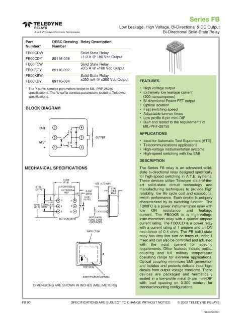
FB00FCY - Teledyne Relays
FB00FCY - Teledyne Relays
FB00FCY - Teledyne Relays

You also want an ePaper? Increase the reach of your titles
YUMPU automatically turns print PDFs into web optimized ePapers that Google loves.
Series FB<br />
Low Leakage, High Voltage, Bi-Directional & DC Output<br />
Bi-Directional Solid-State Relay<br />
Part<br />
DESC Drawing Relay Description<br />
Number* Number<br />
FB00CDW<br />
Solid State Relay<br />
FB00CDY 89116-006<br />
±1.0 A @ ±80 Vdc Output<br />
FB00FCW<br />
Solid State Relay<br />
<strong>FB00FCY</strong> 89116-002<br />
±0.5 A @ ±180 Vdc Output<br />
FB00KBW<br />
Solid State Relay<br />
FB00KBY 89116-004<br />
±250 mA @ ±350 Vdc Output<br />
* The Y suffix denotes parameters tested to MIL-PRF-28750<br />
specifications. The W suffix denotes parameters tested to <strong>Teledyne</strong><br />
specifications.<br />
BLOCK DIAGRAM<br />
FEATURES<br />
• High voltage output<br />
• Extremely low leakage current<br />
(200 nanoamperes)<br />
• Bi-directional Power FET output<br />
• Optical isolation<br />
• Fast switching speed<br />
• Adjustable turn-on times<br />
• Low profile 6-pin mini-DIP<br />
• Built and tested to the requirements of<br />
MIL-PRF-28750<br />
APPLICATIONS<br />
• Ideal for Automatic Test Equipment (ATE)<br />
• Telecommunications applications<br />
• High-voltage instrumentation systems<br />
• High-speed switching with low EMI<br />
DESCRIPTION<br />
MECHANICAL SPECIFICATIONS<br />
DIMENSIONS ARE SHOWN IN INCHES (MILLIMETERS)<br />
The Series FB relay is an advanced solidstate<br />
bi-directional relay designed specifically<br />
for high-speed switching in A.T.E. systems.<br />
These devices utilize <strong>Teledyne</strong> state-of-theart<br />
solid-state circuit technology and<br />
manufacturing techniques to provide high<br />
reliability, low life cycle cost and exceptional<br />
switch performance. Each device is uniquely<br />
characterized by its switching function. The<br />
FB00FC is a power instrumentation relay with<br />
low ON resistance and leakage<br />
current. The FB00KB is a high-voltage<br />
instrumentation relay with a quarter ampere<br />
current rating. The FB00CD is a power relay<br />
with a current rating of 1 ampere and an ON<br />
resistance of 0.4 ohm. The FB solid-state<br />
relay has very fast turn on times of under 1<br />
msec and can also be controlled and adjusted<br />
with the input current for specific<br />
requirements. Other features include optical<br />
coupling and full military temperature<br />
operating range for extreme applications.<br />
Optical coupling minimizes EMI generation<br />
and isolates and protects delicate input logic<br />
circuits from output voltage transients. These<br />
devices are packaged and hermetically<br />
sealed in a low-profile metal 6- pin mini-DIP<br />
with lead spacing on 0.300 centers for<br />
standard mounting configurations.<br />
FB 90 SPECIFICATIONS ARE SUBJECT TO CHANGE WITHOUT NOTICE © 2002 TELEDYNE RELAYS<br />
FB\072002\Q1
Series FB<br />
ELECTRICAL SPECIFICATIONS<br />
(-55°C TO 120°C Ambient Temperature Unless Otherwise Noted)<br />
INPUT (CONTROL) SPECIFICATION<br />
(See Note 1) Min Typ Max Units<br />
Rated Input Current 10 25 mAdc<br />
Input Voltage Drop @ 25 mA 3.25 Vdc<br />
Continuous Input Current<br />
-55°C < T A<br />
< 105°C 10 50 mAdc<br />
105°C < T A<br />
< 120°C 10 25 mAdc<br />
Reverse Voltage Protection -5 Vdc<br />
ENVIRONMENTAL SPECIFICATIONS<br />
Min Max Units<br />
Temperature<br />
Operating -55 +120 °C<br />
Storage -55 +125 °C<br />
Vibration, 100 g 10 2000 Hz<br />
Constant Acceleration 5000 g<br />
Shock, 0.5 ms pulse 1500 g<br />
Input Current (Guaranteed Off) 10 µAdc<br />
Input Current (Guaranteed On) 10 mA<br />
Turn-Off Voltage 1.5 Vdc<br />
OUTPUT (LOAD) SPECIFICATIONS<br />
BI-DIRECTIONAL AND AC CONFIGURATIONS (PIN 4 TO PIN 6), SEE NOTE 2<br />
FB00CD FB00FC FB00KB<br />
Min Max Min Max Min Max Units<br />
Continuous Load Current (See Fig. 3 & Note 5) ±1.0 ±0.5 ±0.25 Adc<br />
Leakage Current @ V load<br />
= max. operating voltage<br />
-55°C < T A<br />
< +25°C ±200 ±200 ±200 nAdc<br />
+25°C < T A<br />
< 120°C ±20 ±20 ±20 µAdc<br />
Output Voltage Drop ±0.75 ±1.0 ±2.4 Vdc<br />
Continuous Operating Load Voltage ±80 ±180 ±350 Vdc<br />
Transient Blocking Voltage (5 s max.) ±90 ±180 ±360 Vdc<br />
ON Resistance R ds<br />
(on) at T J<br />
= 25°C 0.6 1.0 8.0 Ohm<br />
I LOAD<br />
= 100 mAdc (See Fig. 4 & Note 6)<br />
Turn-On Time @ I IN<br />
= 25 mA (See Fig. 2 and 5) 800 800 500 µs<br />
Turn-Off Time (See Fig. 5) 500 500 500 µs<br />
dV/dt 100 100 100 V/µs<br />
Load Surge Current (See Note 3) ±3.5 ±1.75 ±0.875 Adc<br />
DC Offset Voltage 100 100 100 µV<br />
Output Capacitance at 25 Vdc, 1 MHz 325 250 100 pF<br />
© 2002 TELEDYNE RELAYS (800) 284-7007 • www.teledynerelays.com FB 91<br />
FB\072002\Q1
Series FB<br />
OUTPUT (LOAD) SPECIFICATIONS<br />
DC Configuration (Pins 4 and 6 connected together referenced to Pin 5) (See Notes 2 & 7)<br />
FB00CD FB00FC FB00KB<br />
Min Max Min Max Min Max Units<br />
Continuous Load Current (See Fig. 3 & Note 5) 2.0 1.0 0.5 Adc<br />
Leakage Current @ V load<br />
= max. operating voltage<br />
-55°C < T A<br />
< +25°C 400 400 400 nAdc<br />
+25°C < T A<br />
< 120°C 40 40 40 µAdc<br />
Output Voltage Drop 0.4 0.5 1.8 Vdc<br />
Continuous Operating Load Voltage 80 180 350 Vdc<br />
Transient Blocking Voltage (5 s max.) 90 180 360 Vdc<br />
ON Resistance R ds<br />
(on) at T J<br />
= 25°C 0.15 0.25 2.0 Ohm<br />
I LOAD<br />
= 100 mAdc (See Fig. 4 & Note 6)<br />
Turn-On Time @ I IN<br />
= 25 mA (See Fig. 2 and 5) 800 800 500 µs<br />
Turn-Off Time (See Fig. 5) 500 500 500 µs<br />
Load Surge Current (See Note 3) 7.0 3.5 1.75 Adc<br />
Output Capacitance at 25 Vdc, 1 MHz 650 500 200 pF<br />
OUTPUT (LOAD) SPECIFICATIONS<br />
FB00CD FB00FC FB00KB<br />
All Configurations Min Max Min Max Min Max Units<br />
Input to Output Capacitance 5 5 5 pF<br />
Dielectric Strength 500 500 500 Vac<br />
Insulation Resistance @ 500 Vdc 10 9 10 9 10 9 Ohm<br />
Output Junction Temperature @ I LOAD<br />
= I max rated<br />
125 125 125 °C<br />
Maximum Junction Temperature (T J<br />
Max.) 150 150 150 °C<br />
Thermal Resistance Junction to Ambient (θ JA<br />
) 110 110 110 °C/W<br />
Thermal Resistance Junction to Case (θ JC<br />
) 20 20 20 °C/W<br />
FB 92 SPECIFICATIONS ARE SUBJECT TO CHANGE WITHOUT NOTICE © 2002 TELEDYNE RELAYS<br />
FB\072002\Q1
Series FB<br />
A) BI-DIRECTIONAL AND DC CONFIGURATION (SEE NOTE 4)<br />
LOAD CURRENT DERATING CURVE<br />
FIGURE 3<br />
B) DC CONFIGURATION (SEE NOTE 4)<br />
WIRING CONFIGURATIONS<br />
FIGURE 1<br />
INPUT CURRENT VS TURN-ON TIME<br />
FIGURE 2<br />
NORMALIZED ON RESISTANCE VS JUNCTION<br />
TEMPERATURE.<br />
FIGURE 4 (SEE NOTE 6)<br />
NOTES:<br />
1. Series resistor required to limit input current to 50 mA<br />
max.<br />
2. The rated input current is 25 mA for all tests unless<br />
otherwise specified.<br />
3. Surge current is specified for 25°C, 10 cycles maximum at<br />
a 1 Hz repetition rate with 10% duty cycle and 0.1 s.<br />
duration.<br />
4. <strong>Relays</strong> may drive loads connected to either positive or<br />
negative referenced power supply lines. Inductive loads<br />
must be diode suppressed.<br />
5. Continuous load current is rated under the condition of still<br />
air.<br />
6. To calculate the maximum ON resistance for a given<br />
junction temperature, find the normalized ON resistance<br />
factor (NR) from Figure 4. Calculate the new ON<br />
resistance as follows:<br />
R (ON)<br />
= NR X R (ON)<br />
@ 25°C<br />
7. <strong>Relays</strong> are tested in the bi-directional configuration only.<br />
OUTPUT TURN-ON AND OFF TIMING<br />
FIGURE 5<br />
© 2002 TELEDYNE RELAYS (800) 284-7007 • www.teledynerelays.com FB 93<br />
FB\072002\Q1