2SK1736 - ClassicCMP
2SK1736 - ClassicCMP
2SK1736 - ClassicCMP

You also want an ePaper? Increase the reach of your titles
YUMPU automatically turns print PDFs into web optimized ePapers that Google loves.
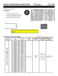
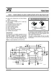
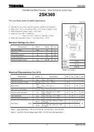
Ordering number:EN3831<br />
N-Channel Silicon MOSFET<br />
<strong>2SK1736</strong><br />
Ultrahigh-Speed Switching Applications<br />
Features<br />
· Low ON resistance.<br />
· Ultrahigh-speed switching.<br />
· Low-voltage drive.<br />
Package Dimensions<br />
unit:mm<br />
2087A<br />
6.9<br />
[<strong>2SK1736</strong>]<br />
1.45<br />
2.5<br />
1.0<br />
1.0<br />
4.5<br />
1.0<br />
Specifications<br />
Absolute Maximum Ratings at Ta = 25˚C<br />
Parameter<br />
Symbol<br />
Drain-to-Source<br />
Voltage<br />
VDSS<br />
100<br />
V<br />
Gate-to-Source<br />
Voltage<br />
VGSS<br />
± 15<br />
V<br />
Drain<br />
Current (DC)<br />
I D 1 A<br />
Drain<br />
Current (Pulse)<br />
IDP<br />
PW≤10µs, duty cycle≤1%<br />
4 A<br />
Allowable<br />
Power Dissipation<br />
P D 1 W<br />
Channel<br />
Temperature<br />
Storage<br />
Temperature<br />
Tch<br />
Tstg<br />
150<br />
–55 to +150<br />
˚C<br />
˚C<br />
Electrical Characteristics at Ta = 25˚C<br />
Parameter<br />
Symbol<br />
Conditions<br />
Conditions<br />
Ratings<br />
1 : Source<br />
2 : Drain<br />
3 : Gate<br />
SANYO : NMP<br />
Drain-to-Source<br />
Breakdown Voltage<br />
V( BR)DSS<br />
I D = 1mA, VGS<br />
100<br />
V<br />
Z ero-Gate Voltage Drain Current<br />
I DS<br />
S V DS<br />
= 100V, VGS<br />
100<br />
µ A<br />
Gate-to-Source<br />
Leakage Current<br />
IGSS<br />
V GS<br />
= ±12V, VDS<br />
± 10<br />
µ A<br />
C utoff Voltage<br />
V GS(off<br />
) V DS<br />
= 10V, ID= 1mA<br />
1.<br />
0<br />
2.<br />
0 V<br />
F orward Transfer Admittance<br />
| yfs | V DS<br />
= 10V, ID= 500mA<br />
0.<br />
9 1.<br />
5<br />
S<br />
Static Drain-to-Source ON-State Resistance<br />
R DS(on)<br />
I D = 500mA, VGS= 10V<br />
0.<br />
7 0.95<br />
Ω<br />
R DS(on)<br />
I D = 500mA, VGS= 4V<br />
0.95<br />
1.<br />
3 Ω<br />
Continued on next page.<br />
1.0<br />
0.9<br />
2.54<br />
0.6<br />
1 2 3<br />
0.5<br />
2.54<br />
min<br />
Ratings<br />
typ<br />
4.0<br />
0.45<br />
max<br />
Unit<br />
Unit<br />
Any and all SANYO products described or contained herein do not have specifications that can handle<br />
applications that require extremely high levels of reliability, such as life-support systems, aircraft’s<br />
control systems, or other applications whose failure can be reasonably expected to result in serious<br />
physical and/or material damage. Consult with your SANYO representative nearest you before using<br />
any SANYO products described or contained herein in such applications.<br />
SANYO assumes no responsibility for equipment failures that result from using products at values that<br />
exceed, even momentarily, rated values (such as maximum ratings, operating condition ranges,or other<br />
parameters) listed in products specifications of any and all SANYO products described or contained<br />
herein.<br />
SANYO Electric Co.,Ltd. Semiconductor Company<br />
TOKYO OFFICE Tokyo Bldg., 1-10, 1 Chome, Ueno, Taito-ku, TOKYO, 110-8534 JAPAN<br />
61599TH (KT)/12693TH (KOTO) A8-7602 No.3831–1/4
<strong>2SK1736</strong><br />
Continued from preceding page.<br />
Input<br />
Capacitance<br />
Output<br />
Capacitance<br />
Parameter<br />
Reverse<br />
Transfer Capacitance<br />
Symbol<br />
Ciss<br />
Coss<br />
Crss<br />
T urn-ON Delay Time<br />
t d(on<br />
)<br />
ise Time<br />
Conditions<br />
Ratings<br />
Unit<br />
V DS<br />
= 20V, f=1MHz<br />
150<br />
pF<br />
V DS<br />
= 20V, f=1MHz<br />
35<br />
pF<br />
V DS<br />
= 20V, f=1MHz<br />
6 pF<br />
See<br />
specified Test Circuit<br />
6 ns<br />
R t r See<br />
specified Test Circuit<br />
10<br />
ns<br />
T urn-OFF Delay Time<br />
t d(off<br />
)<br />
all Time<br />
See<br />
specified Test Circuit<br />
65<br />
ns<br />
F t f See<br />
specified Test Circuit<br />
20<br />
ns<br />
Diode<br />
Forward Voltage<br />
V SD<br />
I S = 1A, VGS<br />
= 0<br />
0.<br />
9<br />
V<br />
Switching Time Test Circuit<br />
No.3831–2/4
<strong>2SK1736</strong><br />
No.3831–3/4
<strong>2SK1736</strong><br />
Specifications of any and all SANYO products described or contained herein stipulate the performance,<br />
characteristics, and functions of the described products in the independent state, and are not guarantees<br />
of the performance, characteristics, and functions of the described products as mounted in the customer's<br />
products or equipment. To verify symptoms and states that cannot be evaluated in an independent device,<br />
the customer should always evaluate and test devices mounted in the customer's products or equipment.<br />
SANYO Electric Co., Ltd. strives to supply high-quality high-reliability products. However, any and all<br />
semiconductor products fail with some probability. It is possible that these probabilistic failures could<br />
give rise to accidents or events that could endanger human lives, that could give rise to smoke or fire,<br />
or that could cause damage to other property. When designing equipment, adopt safety measures so<br />
that these kinds of accidents or events cannot occur. Such measures include but are not limited to protective<br />
circuits and error prevention circuits for safe design, redundant design, and structural design.<br />
In the event that any or all SANYO products(including technical data,services) described or<br />
contained herein are controlled under any of applicable local export control laws and regulations,<br />
such products must not be exported without obtaining the export license from the authorities<br />
concerned in accordance with the above law.<br />
No part of this publication may be reproduced or transmitted in any form or by any means, electronic or<br />
mechanical, including photocopying and recording, or any information storage or retrieval system,<br />
or otherwise, without the prior written permission of SANYO Electric Co., Ltd.<br />
Any and all information described or contained herein are subject to change without notice due to<br />
product/technology improvement, etc. When designing equipment, refer to the "Delivery Specification"<br />
for the SANYO product that you intend to use.<br />
Information (including circuit diagrams and circuit parameters) herein is for example only ; it is not<br />
guaranteed for volume production. SANYO believes information herein is accurate and reliable, but<br />
no guarantees are made or implied regarding its use or any infringements of intellectual property rights<br />
or other rights of third parties.<br />
This catalog provides information as of June, 1999. Specifications and information herein are subject to<br />
change without notice.<br />
PS No.3831–4/4