25 + 25W STEREO AMPLIFIER WITH MUTE/ST-BY - ClassicCMP
25 + 25W STEREO AMPLIFIER WITH MUTE/ST-BY - ClassicCMP
25 + 25W STEREO AMPLIFIER WITH MUTE/ST-BY - ClassicCMP

You also want an ePaper? Increase the reach of your titles
YUMPU automatically turns print PDFs into web optimized ePapers that Google loves.
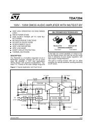
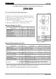
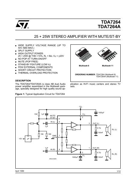
®TDA7264TDA7264A<strong>25</strong> + <strong>25</strong>W <strong><strong>ST</strong>EREO</strong> <strong>AMPLIFIER</strong> <strong>WITH</strong> <strong>MUTE</strong>/<strong>ST</strong>-<strong>BY</strong>WIDE SUPPLY VOLTAGE RANGE (UP TO50V ABS MAX.)SPLIT SUPPLYHIGH OUTPUT POWER:<strong>25</strong> + <strong>25</strong>W @ THD =10%, RL = 8Ω, VS = +20VNO POP AT TURN-ON/OFF<strong>MUTE</strong> (POP FREE)<strong>ST</strong>AND-<strong>BY</strong> FEATURE (LOW IQ)FEW EXTERNAL COMPONENTSSHORT CIRCUIT PROTECTIONTHERMAL OVERLOAD PROTECTIONMultiwatt 8 Multiwatt 11ORDERING NUMBER: TDA7264 (Multiwatt 8)TDA7264A (Multiwatt 11)DESCRIPTIONThe TDA7264/TDA7264A is class AB dual Audiopower amplifier assembled in the Multiwatt package,specially designed for high quality sound applicationas Hi-Fi music centers and stereo TVsets.Figure 1: Typical Application Circuit for TDA726415K 1µF<strong>MUTE</strong>/<strong>ST</strong>-<strong>BY</strong>4+V S2+V S1000µFIN (L)6+3OUT (L)1µF-4.7ΩRL (L)15K18KGND7100nF+5VµP1µFIN (R)D94AU069A8-+1000µF5-V S1OUT (R)4.7Ω100nFRL (R)April 19991/12
TDA7264 - TDA7264AFigure 2: Typical Application Circuit for TDA7264A+V S315K 1µF<strong>MUTE</strong>/<strong>ST</strong>-<strong>BY</strong>51000µFIN (L)7+4OUT (L)1µF-4.7ΩRL (L)15K18KGND9100nF+5VµP1µFIN (R)11-+162OUT (R)4.7ΩRL (R)-V S100nFD98AU9551000µFABSOLUTE MAXIMUM RATINGSSymbol Parameter Value UnitV S DC Supply Voltage 50 VI O Output Peak Current (internally limited) 4.5 AP tot Power Dissipation T case = 70°C 30 WT stg , T j Storage and Junction Temperature -40 to +150 °CPIN CONNECTION (Top view)Multiwatt 8 Multiwatt 118 IN (1)7GND6IN (2)5-V S4<strong>MUTE</strong>/<strong>ST</strong>-<strong>BY</strong>3OUTPUT (2)2+V S1OUTPUT (1)1110987654321IN(1)NOT CONNECTEDGNDNOT CONNECTEDIN(2)-V S<strong>ST</strong><strong>BY</strong>/<strong>MUTE</strong>OUTPUT(2)+V SOUTPUT(1)-V <strong>ST</strong>ab connected to pin 5D94AU096TAB CONNECTED TO PIN 6D98AU956THERMAL DATASymbol Description Value UnitR th j-case Thermal Resistance Junction-case Max 2 °C/W2/12
TDA7264 - TDA7264AELECTRICAL CHARACTERI<strong>ST</strong>ICS (Refer to the test circuit, VS + 20V; RL = 8Ω; Rs =50Ω;f = 1KHz; Tamb = <strong>25</strong>°C, unless otherwise specified.)Symbol Parameter Test Condition Min. Typ. Max. UnitV S Supply Range +5 +22.5 VI q Total Quiescent Current 80 130 mAP O Music Output Power (*) THD = 10%; R L = 8Ω ;V S + 22.5V32 WP O Output Power THD = 10%R L = 8Ω ;V S + 16V; R L = 4ΩTHD = 1%R L = 8Ω ;V S + 16V; R L = 4Ω20 <strong>25</strong><strong>25</strong>THD Total Harmonic Distortion R L = 8Ω ; P O = 1W; f = 1KHz 0.02 %R L = 8Ω ;P O = 0.1 to 15W;f = 100Hz to 15KHz0.5 %C T Cross Talk f = 1KHzf = 10KHz2020R L = 4Ω ; P O = 1W; f = 1KHz 0.03 %R L = 4Ω ; V S + 16V;P O = 0.1 to 12W;f = 100Hz to 15KHz1 %SR Slew Rate 10 V/µsG V Closed Loop Voltage Gain 29 30 31 dB∆G V Voltage Gain Matching 0.2 dBe N Total Input Noise A Curvef = 20Hz to 22KHz70602.53.5 8R i Input Resistance 15 20 KΩSVR Supply Voltage Rejection fr = 100Hz; Vripple = 0.5VRMS 60 dB(each channel)T j Thermal Shut-down145 °CJunction Temperature<strong>MUTE</strong> FUNCTION [ref: +VS]VT <strong>MUTE</strong> Mute / Play Threshold -7 -6 -5 VA M Mute Attenuation 60 90 dB<strong>ST</strong>AND-<strong>BY</strong> FUNCTION [ref: +VS]VT <strong>ST</strong>-<strong>BY</strong> Stand-by / Mute Threshold -3.5 -2.5 -1.5 VA <strong>ST</strong>-<strong>BY</strong> Stand-by Attenuation 110 dBI q <strong>ST</strong>-<strong>BY</strong> Quiescent Current @ Stand-by 3 mANote :(*) FULL POWER up to. VS = ±22.5V with RL = 8Ω and VS = ±16V with RL = 4ΩMUSIC POWER is the maximal power which the amplifier is capable of producing across the rated load resistance (regardless of non linearity)1 sec after the application of a sinusoidal input signal of frequency 1KHz.WWWWdBdBµVµV3/12
TDA7264 - TDA7264AFigure 3: Demo Board Schematic TDA7264R1R215KQ1C31µFC1 1µF<strong>MUTE</strong>/<strong>ST</strong>-<strong>BY</strong>IN (L)46++V S2+V S3OUT (L)C41000µFC5100nFSW1<strong>ST</strong>-<strong>BY</strong>DZR415KSW2<strong>MUTE</strong>R318KGND7-R54.7ΩC8100nFRL (L)C2 1µFIN (R)D94AU068B8-+C7100nF5-V S1C61000µFOUT (R)R64.7ΩC9100nFRL (R)Figure 3a: P.C. Board And Component Layout of the Demo Board Schematic TDA7264 (1:1 Scale)4/12
TDA7264 - TDA7264AFigure 4: Demo Board Schematic TDA7264AR1R2Q1C3<strong>MUTE</strong>/<strong>ST</strong>-<strong>BY</strong>IN (L)57++V S3+V S4C4OUT (L)C5SW1<strong>ST</strong>-<strong>BY</strong>DZC1-R7RL (L)R4R3GND9C8SW2<strong>MUTE</strong>C2IN (R)11-+162OUT (R)R10RL (R)-V SC9D98AU957C7C6Figure 4a: P.C. Board And Component Layout of the Demo Board Schematic TDA7264A (1:1 Scale)TDA7264A5/12
TDA7264 - TDA7264AAPPLICATIONS SUGGE<strong>ST</strong>ION for TDA7264(Demo Board Schematic)The recommended values of the external componentsare those shown on the demo board schematic.Different values can be used: the followingtable can help the designer.COMPONENTSRECOMMENDEDVALUEPURPOSELARGER THANRECOMMENDED VALUESMALLER THANRECOMMENDED VALUER1 10KΩ Mute CircuitIncrease of DzBiasing CurrentR2 15KΩ Mute Circuit Vpin # 4 Shifted Downward Vpin # 4 Shifted UpwardR3 18KΩ Mute Circuit Vpin # 4 Shifted Upward Vpin # 4 Shifted DownwardR4 15KΩ Mute Circuit Vpin # 4 Shifted Upward Vpin # 4 Shifted DownwardR5, R6 4.7Ω Frequency Stability Danger of Oscillations Danger of OscillationsC1, C2 1µFC3 1µFC4, C6 1000µFInput DCDecouplingSt-By/Mute TimeConstantSupply VoltageBypassC5, C7 0.1µFSupply VoltageBypassC8, C9 0.1µF Frequency StabilityDz 5.1V Mute CircuitQ1 BC107 Mute CircuitCOMPONENTSRECOMMENDEDVALUEPURPOSELarger On/Off TimeLARGER THANRECOMMENDED VALUEHigher Low FrequencyCutoffSmaller On/Off TimeDanger of OscillationsDanger of OscillationsSMALLER THANRECOMMENDED VALUER1 10KΩ Mute CircuitIncrease of DzBiasing CurrentR2 15KΩ Mute Circuit Vpin # 5 Shifted Downward Vpin # 5 Shifted UpwardR3 18KΩ Mute Circuit Vpin # 5 Shifted Upward Vpin # 5 Shifted DownwardR4 15KΩ Mute Circuit Vpin # 5 Shifted Upward Vpin # 5 Shifted DownwardR7, R10 4.7Ω Frequency Stability Danger of Oscillations Danger of OscillationsC1, C2 1µFC3 1µFC4, C6 1000µFInput DCDecouplingSt-By/Mute TimeConstantSupply VoltageBypassC5, C7 0.1µFSupply VoltageBypassC8, C9 0.1µF Frequency StabilityDz 5.1V Mute CircuitQ1 BC107 Mute CircuitAPPLICATIONS SUGGE<strong>ST</strong>ION for TDA7264A(Demo Board Schematic)The recommended values of the external componentsare those shown are the demo board schematicdifferent values can be used: the followingtable can help the designer.Larger On/Off TimeHigher Low FrequencyCutoffSmaller On/Off TimeDanger of OscillationsDanger of Oscillations<strong>MUTE</strong>, <strong>ST</strong>AND-<strong>BY</strong> TRUTH TABLESW1SW2A A <strong>ST</strong>AND-<strong>BY</strong>A B <strong>ST</strong>AND-<strong>BY</strong>B B <strong>MUTE</strong>B A PLAY6/12
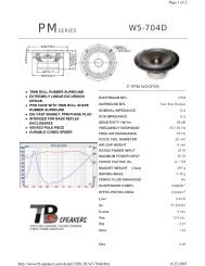
TDA7264 - TDA7264AFigure 5: Quiescent Current vs. Supply VoltageFigure 6: Frequency ResponseFigure 7: Output Power vs Supply VoltageFigure 8: Distortion vs. Output PowerFigure 9: Crosstalk vs. FrequencyFigure 10: Supply Voltage Rejection vs. Fequency7/12
TDA7264 - TDA7264AFigure 11: Attenuation & Total Quiescent Currentvs. Vpin4 VoltageFigure 12: Power Dissipation vs. Output Power8/12
TDA7264 - TDA7264A<strong>MUTE</strong> <strong>ST</strong>AND-<strong>BY</strong> FUNCTIONThe pin 4 (<strong>MUTE</strong>/<strong>ST</strong>AND-<strong>BY</strong>) controls the amplifierstatus by two different thresholds, referred to+VS.- When Vpin4 higher than = +VS - 2.5V theamplifier is in Stand-by mode and the finalstage generators are off- when Vpin4 is between +VS - 2.5V and +VS- 6V the final stage current generators areswitched on and the amplifier is in mutemode- when Vpin4 is lower than +VS - 6V the amplifieris play mode.Figure 13+V S(V)20t-V S-20V IN(mV)Vpin4(V)V SV S -2.5V S- 6V S -10I q(mA)0VOUT(V)OFF<strong>ST</strong>D<strong>BY</strong>PLAY <strong>ST</strong>D<strong>BY</strong> PLAY OFF<strong>ST</strong>D<strong>BY</strong><strong>MUTE</strong> D94AU084 <strong>MUTE</strong> <strong>MUTE</strong> <strong>MUTE</strong>9/12
TDA7264 - TDA7264ADIM.mminchMIN. TYP. MAX. MIN. TYP. MAX.A 5 0.197B 2.65 0.104C 1.6 0.063E 0.49 0.55 0.019 0.022F 0.78 0.85 0.030 0.033G 2.40 2.54 2.68 0.094 0.10 0.105G1 17.64 17.78 17.92 0.69 0.70 0.71H1 19.6 0.772H2 20.2 0.795L 20.35 20.65 0.80 0.81L2 17.05 17.20 17.35 0.67 0.68 0.68L3 17.<strong>25</strong> 17.5 17.75 0.679 0.689 0.699L4 10.3 10.7 10.9 0.406 0.421 0.429L7 2.65 2.9 0.104 0.114S 1.9 2.6 0.075 0.102S1 1.9 2.6 0.075 0.102U 0.40 0.55 0.015 0.022Z 0.70 0.85 0.028 0.034Dia1 3.65 3.85 0.144 0.152OUTLINE ANDMECHANICAL DATAMultiwatt8 (Pin. 5 Gnd)10/12
TDA7264 - TDA7264ADIM.mminchMIN. TYP. MAX. MIN. TYP. MAX.A 5 0.197B 2.65 0.104C 1.6 0.063D 1 0.039E 0.49 0.55 0.019 0.022F 0.88 0.95 0.035 0.037G 1.45 1.7 1.95 0.057 0.067 0.077G1 16.75 17 17.<strong>25</strong> 0.659 0.669 0.679H1 19.6 0.772H2 20.2 0.795L 21.9 22.2 22.5 0.862 0.874 0.886L1 21.7 22.1 22.5 0.854 0.87 0.886L2 17.4 18.1 0.685 0.713L3 17.<strong>25</strong> 17.5 17.75 0.679 0.689 0.699L4 10.3 10.7 10.9 0.406 0.421 0.429L7 2.65 2.9 0.104 0.114M 4.<strong>25</strong> 4.55 4.85 0.167 0.179 0.191M1 4.73 5.08 5.43 0.186 0.200 0.214S 1.9 2.6 0.075 0.102S1 1.9 2.6 0.075 0.102Dia1 3.65 3.85 0.144 0.152OUTLINE ANDMECHANICAL DATAMultiwatt11 V11/12
TDA7264 - TDA7264AInformation furnished is believed to be accurate and reliable. However, <strong>ST</strong>Microelectronics assumes no responsibility for the consequencesof use of such information nor for any infringement of patents or other rights of third parties which may result from its use. No license isgranted by implication or otherwise under any patent or patent rights of <strong>ST</strong>Microelectronics. Specification mentioned in this publication aresubject to change without notice. This publication supersedes and replaces all information previously supplied. <strong>ST</strong>Microelectronics productsare not authorized for use as critical components in life support devices or systems without express written approval of <strong>ST</strong>Microelectronics.The <strong>ST</strong> logo is a registered trademark of <strong>ST</strong>Microelectronics© 1999 <strong>ST</strong>Microelectronics – Printed in Italy – All Rights Reserved<strong>ST</strong>Microelectronics GROUP OF COMPANIESAustralia - Brazil - Canada - China - France - Germany - Italy - Japan - Korea - Malaysia - Malta - Mexico - Morocco - The Netherlands -Singapore - Spain - Sweden - Switzerland - Taiwan - Thailand - United Kingdom - U.S.A.http://www.st.com12/12