TL074, TL074CN LOW NOISE QUAD JFET OP-AMPS - AmpsLab.com
TL074, TL074CN LOW NOISE QUAD JFET OP-AMPS - AmpsLab.com
TL074, TL074CN LOW NOISE QUAD JFET OP-AMPS - AmpsLab.com
- No tags were found...

Create successful ePaper yourself
Turn your PDF publications into a flip-book with our unique Google optimized e-Paper software.
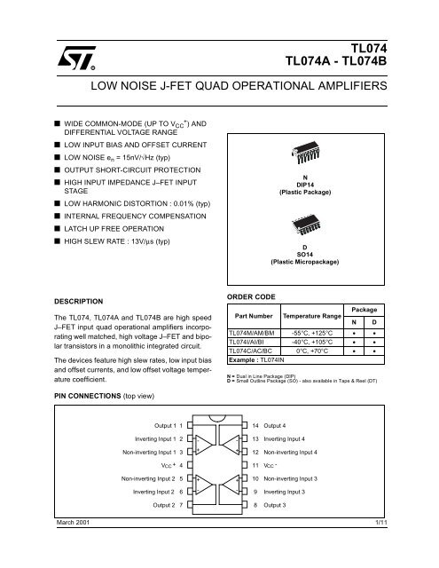
<strong>TL074</strong><strong>TL074</strong>A - <strong>TL074</strong>B<strong>LOW</strong> <strong>NOISE</strong> J-FET <strong>QUAD</strong> <strong>OP</strong>ERATIONAL AMPLIFIERS■ WIDE COMMON-MODE (UP TO V + CC ) ANDDIFFERENTIAL VOLTAGE RANGE■ <strong>LOW</strong> INPUT BIAS AND OFFSET CURRENT■ <strong>LOW</strong> <strong>NOISE</strong> e n = 15nV/√Hz (typ)■ OUTPUT SHORT-CIRCUIT PROTECTION■ HIGH INPUT IMPEDANCE J–FET INPUTSTAGE■ <strong>LOW</strong> HARMONIC DISTORTION : 0.01% (typ)■ INTERNAL FREQUENCY COMPENSATION■ LATCH UP FREE <strong>OP</strong>ERATION■ HIGH SLEW RATE : 13V/µs (typ)NDIP14(Plastic Package)DSO14(Plastic Micropackage)DESCRIPTIONThe <strong>TL074</strong>, <strong>TL074</strong>A and <strong>TL074</strong>B are high speedJ–FET input quad operational amplifiers incorporatingwell matched, high voltage J–FET and bipolartransistors in a monolithic integrated circuit.The devices feature high slew rates, low input biasand offset currents, and low offset voltage temperaturecoefficient.ORDER CODEPackagePart Number Temperature RangeN D<strong>TL074</strong>M/AM/BM -55°C, +125°C • •<strong>TL074</strong>I/AI/BI -40°C, +105°C • •<strong>TL074</strong>C/AC/BC 0°C, +70°C • •Example : <strong>TL074</strong>INN = Dual in Line Package (DIP)D = Small Outline Package (SO) - also available in Tape & Reel (DT)PIN CONNECTIONS (top view)Output 1114Output 4Inverting Input 12--13Inverting Input 4Non-inverting Input 13++12Non-inverting Input 4V CC + 411 VCC -Non-inverting Input 2Inverting Input 256+-+-109Non-inverting Input 3Inverting Input 3Output 278Output 3March 20011/11
<strong>TL074</strong>- <strong>TL074</strong>A - <strong>TL074</strong>BINPUT BIAS CURRENT versus FREE AIRTEMPERATURELARGE SIGNAL DIFFERENTIAL VOLTAGEAMPLIFICATION versus FREE AIR TEMP.INPUT BIAS CURRENT (nA)100V CC = 15V1010.10.01-50 -25 0 25 50 75 100 125TEMPERATURE (˚C)DIFFERENTIAL VOLTAGEAMPLIFICATION (V/V)1000400200100402010421V CC = 15VV O = 10VR = 2k Ω L-75 -50 -25 0 25 50 75 100 125TEMPERATURE (˚C)LARGE SIGNAL DIFFERENTIAL VOLTAGEAMPLIFICATION AND PHASE SHIFT versusFREQUENCYTOTAL POWER DISSIPATION versus FREE AIRTEMPERATURE TOTAL POWER DISSIPATION (mW)2502252001751501251007550250V CC = 15VNo signalNo load-75 -50 -25 0 25 50 75 100 125TEMPERATURE (˚C)SUPPLY CURRENT PER AMPLIFIER versusFREE AIR TEMPERATURECOMMON MODE REJECTION RATIO versusFREE AIR TEMPERATURESUPPLY CURRENT (mA)2.01.81.61.41.21.00.80.60.40.20V CC = 15VNo signalNo load-75 -50 -25 0 25 50 75 100 125TEMPERATURE (˚C)COMMON MODE MODE REJECTIONRATIO (dB)89R L = 10 kΩ88V CC = 15V8786858483-75 -50 -25 0 25 50 75 100 125TEMPERATURE (˚C)6/11
<strong>TL074</strong> - <strong>TL074</strong>A - <strong>TL074</strong>BVOLTAGE FOL<strong>LOW</strong>ER LARGE SIGNAL PULSERESPONSEOUTPUT VOLTAGE versus ELAPSED TIME OUTPUT VOLTAGE (mV)2824201612840-4OVERSHOOT90%V CC= 15VR10%L = 2k ΩTt amb = +25˚Cr0 0.1 0.2 0.3 0.4 0.5 0.6 0.7TIME ( µs)EQUIVALENT INPUT <strong>NOISE</strong> VOLTAGE versusFREQUENCYTOTAL HARMONIC DISTORTION versusFREQUENCYEQUIVALENT INPUT <strong>NOISE</strong>VOLTAGE (nV/VHz)706050403020V CC = 15VA V = 10R S = 100 ΩT amb = +25˚C10010 40 100 400 1k 4k 10k 40k 100kFREQUENCY (Hz)TOTAL HARMONIC DISTORTION(%)1VV CC0.4CC= = 15V 15VAAV V = = 1 1V V0.1 O O (rms) (rms) = = 6V 6VT amb T0.04 amb = = +25˚C0.010.0040.001100 400 1k 4k 10k 40k 100kFREQUENCY (Hz)7/11
<strong>TL074</strong>- <strong>TL074</strong>A - <strong>TL074</strong>BPARAMETER MEASUREMENT INFORMATIONFigure 1 : Voltage FollowerFigure 2 : Gain-of-10 Inverting Amplifier10k Ωe I1k Ω-1/4<strong>TL074</strong>e oR LC L = 100pFTYPICAL APPLICATIONSAUDIO DISTRIBUTION AMPLIFIERfO= 100kHz-1M Ω1/4<strong>TL074</strong>Output A-Input1µF1/4<strong>TL074</strong>-1/4<strong>TL074</strong>Output B100k Ω1OO µF100k Ω100k Ω100k ΩV CC+-1/4<strong>TL074</strong>Output C8/11
<strong>TL074</strong> - <strong>TL074</strong>A - <strong>TL074</strong>BTYPICAL APPLICATIONS (continued)POSITIVE FEEDBACK BANDPASS FILTER16k Ω16k Ω220pF220pF43k Ω43k ΩInput43k Ω1.5k Ω220pF-1/4<strong>TL074</strong>43k Ω30k Ω-1/4<strong>TL074</strong>43k Ω1.5k Ω220pF-1/4<strong>TL074</strong>43k Ω30k Ω-1/4<strong>TL074</strong>Output BOutput AGroundOUTPUT AOUTPUT BSECOND ORDER BANDPASS FILTERfo = 100kHz; Q = 30; Gain = 16CASCADED BANDPASS FILTERfo = 100kHz; Q = 69; Gain = 169/11
<strong>TL074</strong>- <strong>TL074</strong>A - <strong>TL074</strong>BPACKAGE MECHANICAL DATA14 PINS - PLASTIC DIPMillimetersInchesDim.Min. Typ. Max. Min. Typ. Max.a1 0.51 0.020B 1.39 1.65 0.055 0.065b 0.5 0.020b1 0.25 0.010D 20 0.787E 8.5 0.335e 2.54 0.100e3 15.24 0.600F 7.1 0.280i 5.1 0.201L 3.3 0.130Z 1.27 2.54 0.050 0.10010/11
<strong>TL074</strong> - <strong>TL074</strong>A - <strong>TL074</strong>BPACKAGE MECHANICAL DATA14 PINS - PLASTIC MICR<strong>OP</strong>ACKAGE (SO)LCGc1DM14Fa2Abe3esa1Eb181 7MillimetersInchesDim.Min. Typ. Max. Min. Typ. Max.A 1.75 0.069a1 0.1 0.2 0.004 0.008a2 1.6 0.063b 0.35 0.46 0.014 0.018b1 0.19 0.25 0.007 0.010C 0.5 0.020c145° (typ.)D (1) 8.55 8.75 0.336 0.344E 5.8 6.2 0.228 0.244e 1.27 0.050e3 7.62 0.300F (1) 3.8 4.0 0.150 0.157G 4.6 5.3 0.181 0.208L 0.5 1.27 0.020 0.050M 0.68 0.027S8° (max.)Note : (1) D and F do not include mold flash or protrusions - Mold flash or protrusions shall not exceed 0.15mm (.066 inc) ONLY FOR DATA BOOK.Information furnished is believed to be accurate and reliable. However, STMicroelectronics assumes no responsibility for the consequencesof use of such information nor for any infringement of patents or other rights of third parties which may result from its use. No license is grantedby implication or otherwise under any patent or patent rights of STMicroelectronics. Specifications mentioned in this publication are subjectto change without notice. This publication supersedes and replaces all information previously supplied. STMicroelectronics products are notauthorized for use as critical <strong>com</strong>ponents in life support devices or systems without express written approval of STMicroelectronics.© The ST logo is a registered trademark of STMicroelectronics© 2001 STMicroelectronics - Printed in Italy - All Rights ReservedSTMicroelectronics GROUP OF COMPANIESAustralia - Brazil - China - Finland - France - Germany - Hong Kong - India - Italy - Japan - Malaysia - Malta - MoroccoSingapore - Spain - Sweden - Switzerland - United Kingdom© http://www.st.<strong>com</strong>11/11