2SK369 - Datasheet Catalog
2SK369 - Datasheet Catalog
2SK369 - Datasheet Catalog

Create successful ePaper yourself
Turn your PDF publications into a flip-book with our unique Google optimized e-Paper software.
<strong>2SK369</strong><br />
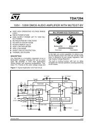
TOSHIBA Field Effect Transistor Silicon N Channel Junction Type<br />
<strong>2SK369</strong><br />
For Low Noise Audio Amplifier Applications<br />
Unit: mm<br />
Suitable for use as first stage for equalizer and MC head amplifiers.<br />
High |Yfs|: |Yfs| = 40 mS (typ.) (VDS = 10 V, VGS = 0, IDSS = 5 mA)<br />
High breakdown voltage: VGDS = −40 V (min)<br />
Super low noise: NF = 1.0dB (typ.)<br />
(VDS = 10 V, ID = 5 mA, f = 1 kHz, RG = 100 Ω)<br />
High input impedance: IGSS = −1 nA (max) (VGS = −30 V)<br />
Maximum Ratings (Ta 25°C)<br />
Characteristics Symbol Rating Unit<br />
Gate-drain voltage V GDS 40 V<br />
Gate current I G 10 mA<br />
Drain power dissipation P D 400 mW<br />
Junction temperature T j 125 °C<br />
Storage temperature range T stg 55~125 °C<br />
JEDEC<br />
JEITA<br />
TOSHIBA<br />
TO-92<br />
SC-43<br />
2-5F1D<br />
Electrical Characteristics (Ta 25°C)<br />
Weight: 0.21 g (typ.)<br />
Characteristics Symbol Test Condition Min Typ. Max Unit<br />
Gate cut-off current I GSS V GS 30 V, V DS 0 1.0 nA<br />
Gate-drain breakdown voltage V (BR) GDS V DS 0, I G 100 A 40 V<br />
Drain current<br />
I DSS<br />
V DS 10 V, V GS 0 5.0 30 mA<br />
(Note 1)<br />
Gate-source cut-off voltage V GS (OFF) V DS 10 V, I D 0.1 A 0.3 1.2 V<br />
Forward transfer admittance<br />
Y fs <br />
V DS 10 V, V GS 0, f 1 kHz,<br />
(I DSS 5 mA)<br />
25 40 mS<br />
Input capacitance C iss V DS 10 V, V GS 0, f 1 MHz 75 pF<br />
Reverse transfer capacitance C rss V GD 10 V, I D 0, f 1 MHz 15 pF<br />
Noise figure (Note 2)<br />
NF (1)<br />
NF (2)<br />
V DS 10 V, R G 100 9, I D 5 mA,<br />
f 100 Hz<br />
V DS 10 V, R G 100 9, I D 5 mA,<br />
f 1 kHz<br />
Note 1: I DSS classification GR: 5.0~10.0 mA, BL: 8.0~16.0 mA, V: 14.0~30.0 mA<br />
Note 2: Use this in the low voltage region (VDS 15 V) for low noise applications.<br />
5 10<br />
1 2<br />
dB<br />
1<br />
2003-03-26
<strong>2SK369</strong><br />
2<br />
2003-03-26
<strong>2SK369</strong><br />
3<br />
2003-03-26
<strong>2SK369</strong><br />
4<br />
2003-03-26
<strong>2SK369</strong><br />
RESTRICTIONS ON PRODUCT USE<br />
000707EAA<br />
TOSHIBA is continually working to improve the quality and reliability of its products. Nevertheless, semiconductor<br />
devices in general can malfunction or fail due to their inherent electrical sensitivity and vulnerability to physical<br />
stress. It is the responsibility of the buyer, when utilizing TOSHIBA products, to comply with the standards of<br />
safety in making a safe design for the entire system, and to avoid situations in which a malfunction or failure of<br />
such TOSHIBA products could cause loss of human life, bodily injury or damage to property.<br />
In developing your designs, please ensure that TOSHIBA products are used within specified operating ranges as<br />
set forth in the most recent TOSHIBA products specifications. Also, please keep in mind the precautions and<br />
conditions set forth in the “Handling Guide for Semiconductor Devices,” or “TOSHIBA Semiconductor Reliability<br />
Handbook” etc..<br />
The TOSHIBA products listed in this document are intended for usage in general electronics applications<br />
(computer, personal equipment, office equipment, measuring equipment, industrial robotics, domestic appliances,<br />
etc.). These TOSHIBA products are neither intended nor warranted for usage in equipment that requires<br />
extraordinarily high quality and/or reliability or a malfunction or failure of which may cause loss of human life or<br />
bodily injury (“Unintended Usage”). Unintended Usage include atomic energy control instruments, airplane or<br />
spaceship instruments, transportation instruments, traffic signal instruments, combustion control instruments,<br />
medical instruments, all types of safety devices, etc.. Unintended Usage of TOSHIBA products listed in this<br />
document shall be made at the customer’s own risk.<br />
The information contained herein is presented only as a guide for the applications of our products. No<br />
responsibility is assumed by TOSHIBA CORPORATION for any infringements of intellectual property or other<br />
rights of the third parties which may result from its use. No license is granted by implication or otherwise under<br />
any intellectual property or other rights of TOSHIBA CORPORATION or others.<br />
The information contained herein is subject to change without notice.<br />
5<br />
2003-03-26
This datasheet has been download from:<br />
www.datasheetcatalog.com<br />
<strong>Datasheet</strong>s for electronics components.