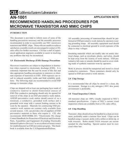
AN-1001 - California Eastern Laboratories
AN-1001 - California Eastern Laboratories
AN-1001 - California Eastern Laboratories

You also want an ePaper? Increase the reach of your titles
YUMPU automatically turns print PDFs into web optimized ePapers that Google loves.
<strong>California</strong> <strong>Eastern</strong> <strong>Laboratories</strong><br />
<strong>AN</strong>-<strong>1001</strong><br />
RECOMMENDED H<strong>AN</strong>DLING PROCEDURES FOR<br />
MICROWAVE TR<strong>AN</strong>SISTOR <strong>AN</strong>D MMIC CHIPS<br />
INTRODUCTION<br />
APPLICATION NOTE<br />
This document is provided to inform users of some of the<br />
handling precautions necessary and the assembly processes<br />
recommended in order to successfully use NEC microwave<br />
transistor and MMIC chips. Those who are unable to achieve<br />
satisfactory assembly results are encouraged to contact a CEL<br />
sales office for further assistance. CELhas a staff of experienced<br />
application engineers available to assist in resolving<br />
any problems that may be encountered.<br />
1.0 Electrostatic Discharge (ESD) Damage Precautions<br />
Microwave transistors are subject to degradation or destruction<br />
when exposed to electrostatic discharge (ESD). It is<br />
extremely important that the user be aware of this fact and<br />
take appropriate handling precautions to minimize or eliminate<br />
exposure of transistors to ESD. ESD exposure can result<br />
in reduced assembly yields and field reliability problems.<br />
The following steps are recommended to avoid ESD<br />
damage to transistor chips.<br />
Chips are shipped with at least one packaging layer made of<br />
conductive material to shield fromextemal sources of<br />
ESD.This conductive packaging should only be opened for<br />
removal of the chips at an ESD preventative work station.<br />
<strong>AN</strong>ESD preventative work station should consist of, as a<br />
minimum, a conductive, grounded work surface and a<br />
grounded wrist strap with a current limiting resistor to be<br />
wom by the operator. Materials for constructing ESD preventative<br />
work stations are commer cially available from<br />
several sources. CEL can provide a list of suppliers of ESD<br />
preventative materials to those who require it. CEL also<br />
recommends DOD-HDBK-263, “Electrostatic Dis charge<br />
Control Handbook for Protection of Electrical and Electronic<br />
Parts, Assemblies and Equipment (Excluding Electrically<br />
Initiated Explosive Devices)” as an excellent ref erence source<br />
for establishmentof an ESD prevention program. This handbook<br />
is available from the U.S.DepartmentofDefense.<br />
All assembly processing of transistorchips should be performed<br />
at ESD preventative work stations by operators wearing<br />
grounding straps. All assembly equipment used should<br />
be connected to electrical ground to avoid exposure of the<br />
chips to stray voltages.<br />
Insulating materials which can readily take on astatic electrical<br />
charge, such as styrofoam, plastic, and nylon, should<br />
be kept away from the vicinity of work stations. ESD preventative<br />
lab coats or smocks should be used to cover clothing<br />
made of synthetic materials wom by operators.<br />
Work in process should be transported and stored in closed<br />
conductive containers. These containers should only be<br />
opened at ESD preventative work stations.<br />
2.0 Chip Storage<br />
It is recommended that all chips be stored in a clean, dry<br />
environment. Storage in a dry nitrogen (-50°C dew point)<br />
environment is preferable.<br />
3.0 Visual Inspection Criteria<br />
All transistor chips are 100% visually inspected to NEC’s<br />
standard specifications. Copies of NEC’s current visual<br />
inspection criteria are available from a CEL sales office.<br />
4.0 Chip Handling<br />
Transistor chips should always be handled in a clean environment,<br />
preferably under a laminar flow hood. Chips can be<br />
handled using a vacuum probe with a teflon or delrin tip, or<br />
with tweezers. Rubis model 5ASA tweezers are recommended<br />
for chip handling. Special caution must be exercised<br />
when han-
dling GaAs FET chips with tweezers. Ga-As is a very brittle<br />
material and edge chip-outs will occur if excessive pressure<br />
is used. GaAs FET chips should be gripped squarely and<br />
lightly with tweezers. See figure 1.<br />
5.0 Die Attach<br />
FIGURE 1<br />
Bipolar transistor chips can be die attached by means of a<br />
colletor with tweezers. Best results are achieved for GaAs<br />
FETchips by using the tweezers, as collets frequently cause<br />
edge damage. Eutectic die attach is recommended, although<br />
epoxy die attach is permissible for small signal or low noise<br />
transistors. The increased thermal resistance resulting from<br />
epoxy die attach must be taken into consideration if this<br />
method is used. Epoxy die attach cannot be recommended<br />
for any power transistors.<br />
Eutectic die attach should be performed in a dry nitrogen<br />
atmosphere to avoid the formation of oxides. A suitable nitrogen<br />
environment can be achieved by directing a 200 liter<br />
per hour flow through a nozzle onto the surface to which the<br />
die will be attached. Forming gas composed of 95% nitrogen,<br />
and 5% hydrogen will reduce organic contaminants on<br />
the substrate surface and may be substituted for dry nitrogen.<br />
All NEC transistor chips have pure gold backside<br />
metallizaton to facilitate achieving good eutectic die attach.<br />
Die attachment is achieved by placing a eutectic preform in<br />
the proper location and then lightly “scrubbing” the chip on<br />
the preform. Silicon devices can also be eutecticly attached<br />
to a gold plated substrate surface widiout the use of preforms<br />
when the gold plating thickness exceeds 100 microinches.<br />
If multiple components must be euctectically attached to a<br />
substrate, the transistor chips should be attached last to minimize<br />
the exposure time at temperature. The total chip exposure<br />
time should be limited to less than 5 minutes at 300°C,<br />
and less than one minute at 400°C. A typical exposure time<br />
of about 30 seconds can be expected for a skilled operator<br />
die attaching small signal transistor chips. The following<br />
listed eutectic alloys and die attach temperatures are recommended<br />
for the various types of NEC microwave transistor<br />
and MMIC chips.<br />
A. NPN Silicon Bipolar Chips and Silicon MMIC Chips:<br />
a) AuSb (0.05% Sb) at 400°C ± 5°C.<br />
b) AuSi (3% Si) at 400°C ± 5°C.<br />
c) Au (100%) at 400°C ± 5°C.<br />
d) AuSi (no preform) at 400°C ± 5°C.<br />
B. PNP Silicon Bipolar Chips<br />
a) Au (100%) at 400°C ± 5°C.<br />
b) AuSi (no preform) at 400°C ± 5°C.<br />
C. GaAs FET Chips and GaAs MMIC Chips:<br />
a) AuSn (20% Sn) at 300°C 5°C.<br />
b) AuGe (8% Ge) at 380°C 5°C.<br />
Special handling procedures are required for power GaAs<br />
FET chips manufactured using NEC’s plated heat sink (PHS)<br />
technology. These chips are large, very thin (60° ±15 µm),<br />
and subject to the possibility of cracking due to the thermal<br />
shock encountered during the die attach process. This problem<br />
can be avoided by using a hot plate to preheat the chips<br />
and substrates to which they are being attached to an intermediate<br />
temperature for 2 minutes prior to placement on the<br />
die attach hot plate. After die attachment is completed, the<br />
reverse process is used for cool-down.<br />
Example when using AuSn eutectic:<br />
Ambient 150°C 300°C 150°C Ambient<br />
Hot Plate Die Attach Hot Plate<br />
Consult the appropriate CEL data sheet to determine if a<br />
power GaAs FET chip employs the PHS process.<br />
5.1 Trouble Shooting the Die Attach Process<br />
A. Using Gold Alloy Preforms<br />
The alloy elements and the percentage content in a preform<br />
will determine the melting temperature of the preform.<br />
Different alloys are available to meet particular<br />
electrical specifications or assembly requirements.<br />
NEC/CEL uses 80% gold and 20% tin preforms with<br />
GaAs MESFETs and Hetero Junction (HJ) FETS. The<br />
working temperature should be well above the preform<br />
melting point so that full wetting can be assured. For this<br />
preform the recommended working temperature is 300<br />
degrees C ± 5 degrees.<br />
All preforms should be stored in a dry nitrogen atmosphere<br />
to prolong their life by keeping them free of contaminants<br />
& oxidation.<br />
1. Contaminated Preforms<br />
Contaminated preforms can only be spotted during the<br />
die attachment process. A bad preform shows signs of a<br />
blackish, dull tint. Sample preforms should be tested<br />
before the die is scrubbed into the preform.<br />
a) Testing<br />
Place several preforms on a carrier. Use dry<br />
nitrogen or forming gas N2H2 (95% / 5% respectively)<br />
to flow evenly over the hot plate at a<br />
rate of 200 liters per hour. A low power zoom<br />
microscope with 7 to 40
magnification will be sufficient to inspect the results.<br />
Place the carrier onto the hot plate and watch the preforms<br />
start to melt (5 to 10 seconds) and spread out the preforms<br />
with a tweezer.<br />
Good Preforms: Will appear shiny and smooth and will<br />
flow smoothly over the carrier surface.<br />
Bad preforms: Will appear dull and wrinkled.<br />
Bad preforms should be either discarded or cleaned.<br />
Buying preforms in small quantities and different lots<br />
assists in eliminating problems.<br />
b) Cleaning<br />
The cleaning method for preforms is the same as for<br />
cleaning a substrate (see section 7. 1). This can be time<br />
consuming and costly. It may be more cost effective to<br />
replace bad preforms.<br />
c) Preform Sizes<br />
Care should be exercised in choosing preforms of proper dimensions.<br />
Oversized preforms can increase costs and reduce<br />
die attach quality due to floating effect. Floating occurs<br />
when the preform is too large and results in poor thermal<br />
contact caused by the chip floating on a bubble of melted<br />
preform. It is best to order preforms that are slightly smaller<br />
than the chip being used and/or allow plenty of scrubbing<br />
space for excess preform material to flow. The recommended<br />
thickness for preforms is .001 inch.<br />
B. Die Attaching Procedure<br />
1. Set preform in position where die is to rest.<br />
2. Place die on same carrier to preheat.<br />
3. Place carrier on hot plate.<br />
4. Wait for preform to melt.<br />
5. Scrub die onto preform - approximate time, 0 to 1<br />
minute.<br />
6. Remove carrier from hot plate and cool on metal<br />
block.<br />
C. Common Die Attach Problems<br />
1. The Back of the Chip Wets 50% or Less<br />
• The back of the chip is contaminated.<br />
• The preforms are contaminated or oxidized.<br />
• There is not enough scrubbing action.<br />
• The process is performed in a non-clean environ<br />
ment.<br />
• Oxides are forming due to insufficient or improper<br />
flow of dry nitrogen or forn-dng gas.<br />
2.The Preform Does Not Wet Properly<br />
• The preform is contaminated or oxidized.<br />
• There is no forming gas or there is an incorrect<br />
mixture.<br />
• The substrate or carrier is contaminated.<br />
6.0 Removal of Particulate from Chip Surface<br />
Foriegn particulate will occasionally be encountered on the<br />
surface of chips due to handling and exposure even when<br />
good procedures are used. In the case of power FET chips<br />
employing the PHS process, small pieces of the gold edge<br />
metallization will occasionally break off and be found on the<br />
surface of the chip or circuit substrate. This phenomenon is<br />
due to the process used to fabricate these chips which leaves<br />
a fragile edge area, but RF performance is not affected by<br />
this.<br />
Such particulate can be removed after die attach by<br />
blowing them off of the chip and circuit surfaces with dry<br />
nitrogen. If this process is not feasible, a vacuum needle<br />
can be used to remove particulate.<br />
6.1 Particulate Contamination Removal from Si and<br />
GaAs Chip Devices<br />
At CEL we used the WASSCO TEL-K-150 Vacuum<br />
System for particulate contamination removal from Si and<br />
GaAs Chip Devices. Any equivalent system can also be<br />
used with satisfactory results. Below is the basic procedure<br />
used by CEL for particle contamination removal.<br />
This can be used as a guide when implementing a system<br />
other than that used by CEL.<br />
1) Bend a Tel-1555 needle tip at the 2/3 length point<br />
at approximately a 45° angle for operator ease in particulate<br />
removal. See Figure 3.<br />
FIGURE 3<br />
2) Viewing the chip to be cleaned under a high power<br />
microscope, position the needle near and above the particulate<br />
contamination without touching the chip surface.<br />
3) The operator then puts his finger over the<br />
vacuum hole in the probe and the partculate is sucked<br />
into the needle and carried away.<br />
4) This is a somewhat delicate process and takes operator<br />
practice to develop the skill to remove contamination<br />
with out scratching and damaging the chips.<br />
Approximately 1 hour per day for 1 week should be<br />
sufficient practice.
7.0 Wire Bond Process<br />
Thermo-compression bonding (TCB)is recommended for<br />
NEC microwave chips. Ball bonding is not recommended<br />
for bond pads smaller than 100 pm square. Ultrasonic bonding<br />
is not recommended because the ultrasonic energy can<br />
cause weakening of the adhesion of the bonding pad<br />
metalization to the chip resulting in lifting of the bonding<br />
pads. Ultrasonic wire bonders can also induce electrostatic<br />
voltages if not properly grounded.<br />
Wire bonding is accomplished by first bonding to the chip<br />
bonding pad, and then to the circuit. Semi-hard gold bond<br />
wire with 3-8% elongation is recommended. 20 lim diameter<br />
wire should be used for all chips with bonding pads of 50 µm<br />
or less in width. 30 µm diameter bond wire is recommended<br />
for those chips with bond pads greater than 70 µm in width.<br />
Bonding should be performed in a dry nitrogen environment<br />
which can be accomplished by directing allow of nitrogen at<br />
100 liters per hour through a nozzle ovor the chip surface.<br />
The best results are achieved for a bond deformation of 1.5<br />
times the wire diameter. A bond deformation of less than 1.2<br />
times the wire diameter will usually result in poor bond-pull<br />
strength, while a bond deformation of two (2) times the wire<br />
diameter is indicative of excess bonding force which may<br />
damage the chip and/or weaken the bond wire at the heel of<br />
the bond. The following wire bonding process conditions<br />
are recommended:<br />
Chip temperature: 240°C ± 5°C<br />
Bonding tool temperature: 180°C ± 5°C<br />
Bonding force: 20-25 grams for 20 µm wire<br />
28-34 grams for 30 µm wire<br />
A bonding wedge of similar dimensions as depicted in Figure<br />
2 is recommended. Such a bonding wedge is available<br />
from Kulicke & Soffa Industries, part number 4200 Special.<br />
7.1 Trouble Shooting The Wire Bond Process<br />
A. Wire Considerations<br />
1. Stabilized vs. Unstabilized Gold Bond Wire For a<br />
given elongation, the break load of stabilized<br />
wire(in grams) can be from 15% to 50% greater<br />
than that of unstabilized wire. NEC recommends<br />
that stabilized wire with 3% - 8% elongation be<br />
used.<br />
2. Tempers of Gold<br />
•Hard - Maximum of gold work.<br />
•Semi-hard - Hardness is partially removed.<br />
•Annealed - All or most of the hardness is<br />
removed.<br />
Semi-hard and Annealed gold wire will show little or<br />
no aging effects at room temperature. Wire which is<br />
stress relieved with a percentage of elongation between<br />
Model 4200 special wedge<br />
F = 0.0017<br />
FR = 0.001<br />
BR = 0.0006<br />
H = 0.0015<br />
W = 0.003<br />
s = 0.010<br />
45 Degree Feed flole<br />
Flat Foot<br />
Length = 0.828<br />
NOTES:<br />
1. Back radius (BR) shall be included in<br />
F dimension unless otherwise specified.<br />
2. ( ) polished finish standard on flat foot, matte finish<br />
standard on concave foot.<br />
3. Funnel shall be centered on foot width (W) within<br />
+ 0004.<br />
4. Larger BR available as an option.<br />
5. All dimensions are in inches<br />
FIGURE 2<br />
3% to 8% will achieve the maximum breaking load to<br />
meet MIL-Stds 750 and 883.<br />
3. Storage<br />
Wire should be kept in a<br />
dry, dust free, air-conditioned environment, free<br />
from hydrocarbons. Storage in dry nitrogen atmo<br />
sphere with temperature controlled be tween 65 to 72<br />
degrees F is recommended.
B. Common Bonding Problems<br />
1. Low Bond Strength Can Result From:<br />
• Contamination films on the wire, chip or<br />
substrate.<br />
• Insufficient bonding temperature.<br />
• Insufficient force on the bonding wedge.<br />
• Bond pad lifting.<br />
a) Contamination Films on the Wire, Chip or<br />
Substrate<br />
Clean the effected surface by:<br />
•Wire - soaking the spool of wire in alcohol.<br />
•Substrates - cleaning in TCE, acetone, and<br />
alcohol for 15 minutes with ultrasonic.<br />
•Chips - Bipolar or GaAs FET chips may be<br />
cleaned by plasma cleaning (ashing) or by use of<br />
alcohol based solvents. Bonding capillaries may<br />
also be cleaned, if they become contaminated, in<br />
ultrasonic using DI WATER only.<br />
b) Insufficient Temperature<br />
Stage temperature can vary from ambient to 300<br />
degrees C depending on the method used to die<br />
attach the chip onto the substrate or carrier.<br />
Epoxies are cured at approximately 150 degrees<br />
C. Preforms flow at 150 degrees C or above,<br />
depending on the per centage of gold used in<br />
eutectic mixture; the more gold, the higher the<br />
temperature. With 80% gold and 20% tin<br />
mixture (CEL’s standard), the stage tempera ture<br />
is controlled to 240 degrees C, slightly below the<br />
melting temperature of the preform.<br />
Tip temperature is completely dependent upon the<br />
bonding machine used. Most machines on the<br />
market today have the capability of temperatures<br />
ranging from ambient to 275°C. CEL controls<br />
the tip temperature at 180°C. The tip temperature<br />
varies inversely with the stage temperature to<br />
achieve a good bond.<br />
2. Bond Pad Peeling<br />
There are two major causes of this problem:<br />
a) Pad peels away cleanly from chip.<br />
This effect is usually due to the use of ultrasonic<br />
bonding machines. The most obvious condition is<br />
when the wedge makes contact with the pad and<br />
causes immediate peeling. If the pad does not peel<br />
immediately, it may peel cleanly during bond pull.<br />
NEC/CEL does not recommend ultrasonic<br />
bonding for any of their devices.<br />
b) Cratering<br />
This condition results in pad peeling with a<br />
cratering effect down into the chip surface. This<br />
is usually caused by too much bonding force.<br />
8.0 Availability of Practice Chips:<br />
Assembly practice chips are available from CEL at reduced<br />
cost for training of operators and development of assembly<br />
processes. it is recommended that these practice chips be used<br />
to develop operator skills prior to attempting circuit assembly<br />
with full specification devices. Contact your local sales<br />
office for more information.<br />
NOTICE<br />
These handling procedures are to be used only as guidelines.<br />
Califomia Eastem <strong>Laboratories</strong> Inc. (CEL) assumes<br />
no liability for customer implimentation of these procedures.<br />
CEL reserves the right to make changes in these<br />
handling procedures without notice.<br />
For thermo-compression bonding, a capillary<br />
made of titanium carbide has proven to have a<br />
longer life when used at high temperatures.<br />
c) Insufficient Force on the Bonding Wedge Bonds<br />
that will not stick to the bonding pad may be<br />
caused by insufficient bonding force or by the<br />
wedge that is used.<br />
*CEL recommends the K & S “4200 Special”<br />
wedge made by Micro-Swiss. This wedge was<br />
designed to accommodate all of NEC’s bond pad<br />
sizes.<br />
<strong>California</strong> <strong>Eastern</strong> <strong>Laboratories</strong><br />
Exclusive Agents for NEC RF, Microwave and Optoelectronic<br />
semiconductor products in the U.S. and Canada<br />
4590 Patrick Henry Drive, Santa Clara, CA 95054-1817<br />
Telephone 408-988-3500 • FAX 408-988-0279 •Telex 34/6393<br />
Internet: http:/WWW.CEL.COM<br />
Information and data presented here is subject to change without notice.<br />
<strong>California</strong> <strong>Eastern</strong> <strong>Laboratories</strong> assumes no responsibility for the use of<br />
any circuits described herein and makes no representations or warranties,<br />
expressed or implied, that such circuits are free from patent infingement.<br />
© <strong>California</strong> <strong>Eastern</strong> <strong>Laboratories</strong> 01/23/2003