AN1035 - California Eastern Laboratories
AN1035 - California Eastern Laboratories
AN1035 - California Eastern Laboratories

You also want an ePaper? Increase the reach of your titles
YUMPU automatically turns print PDFs into web optimized ePapers that Google loves.
<strong>California</strong> <strong>Eastern</strong> <strong>Laboratories</strong><br />
<strong>AN1035</strong><br />
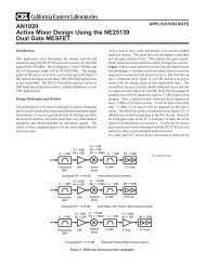
Design Considerations for a Ku-Band DRO<br />
in Digital Communication Systems<br />
APPLICATION NOTE<br />
ABSTRACT<br />
This application note will review the process by which Dielectric<br />
Resonator Oscillator (DRO) designers choose their<br />
oscillator’s topology and devices based on performance requirements,<br />
real estate constraints and manufacturing yields<br />
concerns. DROs are attractive microwave sources because of<br />
their high Q, low phase noise, good output power and high<br />
stability versus temperature. They represent a good compromise<br />
of costs, size, and performance compared to alternative<br />
signal sources such as cavity oscillators, microstrip oscillators<br />
or multiplied crystal oscillators.<br />
Using the local oscillator of a Ku-Band Low Noise Block<br />
(LNB) in a Digital Direct Broadcast System (DDBS) application<br />
as a practical example, this article will demonstrate a<br />
DRO design at 11.25 GHz with one of NEC’s new super low<br />
cost plastic package MESFETs. The required system specifications<br />
as well as the design’s performance will be presented.<br />
The paper then discusses choosing an appropriate device and<br />
how phase noise parameters are included in the nonlinear<br />
model. Upon reviewing basic DRO topologies and focusing<br />
on a reflection type oscillator, the paper proceeds with a linear<br />
and nonlinear simulation using HP-EEsof’s SERIES IV<br />
to accurately predict the DRO performance. Measured results<br />
and practical “on the bench optimization” methods will then<br />
be considered. Finally, as cost is of paramount importance to<br />
designers of commercial products, a total cost summary of<br />
the parts for the DRO and mechanical assembly will be presented.<br />
While the design proposed might not yield the optimum<br />
design solution for all DBS applications, it does introduce<br />
a few important DRO design techniques that can be applied<br />
to other high frequency communication systems.<br />
SPECIFICATIONS<br />
In a DDBS system application, the DRO must exhibit low<br />
phase noise in order to meet the digital modulation scheme<br />
and Bit Error Rate (BER) requirements. It also must have<br />
minimal frequency drift over temperature to keep the receiver<br />
locked into the selected channel and should provide enough<br />
output power to directly drive the mixer downconverter (usually<br />
a diode ring or an active GaAs FET mixer). Because the<br />
DC supply is usually supplied through the IF feed from an<br />
indoor unit, voltage requirements are usually not a constraint<br />
with as much as 8 V available from the system. However,<br />
current draw remains a limitation and needs to be set to the<br />
lowest value that will allow meeting the output power specifications.<br />
Finally, DBS applications drive the need for a design<br />
that is both compact and light since the LNB will be a<br />
small outdoor unit located at the focal point of an antenna<br />
through a light supportive pole. These last needs were met by<br />
using 0603 (60 mils by 30 mils components) SMT technology<br />
components and by laying out the components within a<br />
tightly enclosed cavity. These choices resulted in a .950" by<br />
0.750" by 0.500" final design that also includes the metal<br />
PARAMETER UNITS SPECIFICATION SIMULATION MEASURED<br />
PERFORMANCE<br />
Supply Voltage (V) 8 ± 0.25 6.0 6.0 ± 0.25<br />
Supply Current (mA) 20 ± 2.5 18 18<br />
Operating Frequency Range (GHz) 11.25 11.25 11.25<br />
Output Power (50 ohms) (dBm) 7 ± 2.5 7.2 6.5<br />
Phase Noise at 1 KHz (dBC/Hz) -58 -61.3 -62.8<br />
Phase Noise at 10 KHz (dBC/Hz) -80 -91.3 -89.4<br />
Phase Noise at 30 KHz (dBC/Hz) -90 - -97.6<br />
Phase Noise at 100 KHz (dBC/Hz) -100 -120.4 -112.3<br />
Phase Noise at 1 MHz (dBC/Hz) -120 -131.2 -130.0<br />
Freq. pushing (VCC = 6 V ± 0.25 V) (KHz) ±800 max Not simulated ±200<br />
Freq. pulling (VSWR = 2.0:1 at all phases) (MHz) ±2 Not simulated ±1<br />
Harmonics (dBC) -40 min -20 min -50 min<br />
Spurious (dBC) -80 min N/A -80 min<br />
Output impedance (in a 50 Ω system) N/A VSWR ≤ 2.0:1 Not simulated VSWR ≤ 1.5:1<br />
(With Buffer)<br />
Operating temperature (°C) -55 to +80 Not simulated -55 to +80<br />
Temperature stability (MHz) ±2 Not simulated ±700 KHz<br />
Table 1. Digital DBS DRO: Goal, simulation and test results.
<strong>AN1035</strong><br />
cavity, the tuning screw and output connectors. The enclosed<br />
Table 1 summarizes the design goals, simulated performance<br />
and final laboratory results.<br />
DEVICE CHOICE AND CHARACTERISTICS<br />
Designers of high volume commercial products share common<br />
goals: high performance, small size, low costs and high<br />
manufacturing yields. When choosing a device, the choices<br />
are many: Silicon Bipolars, Si MOSFETs, GaAs FETs or<br />
Gunn/IMPATT diodes [1]. In all cases, to achieve a clean oscillation<br />
and good phase noise performance, the criteria should<br />
include a low noise figure and enough loop gain at the maximum<br />
operating junction temperature and under large signal<br />
conditions. The silicon bipolar is a natural for low noise oscillators<br />
due to its well-characterized and repeatable parameters<br />
and an intrinsic excellent phase noise performance.<br />
However, for any good steady oscillating operation, a good<br />
rule of thumb is to use a transistor with a f T at least two to<br />
three times the operating frequency. These conditions would<br />
require medium output power silicon transistors with a f T<br />
between 23 and 35 GHz. Such devices, currently under development,<br />
are not yet readily available for high volume manufacturing.<br />
However, DRO designs up to X-Band are now easily<br />
attainable with a silicon solution. Because of similar high<br />
frequency requirement, Si MOSFETs are better suited choices<br />
at lower frequencies. Gunn and IMPATT diodes make excellent<br />
very high frequency devices (50 GHz and above), but<br />
their high phase noise, need for careful mechanical design<br />
and very low power efficiency make them an unsuitable choice<br />
for high volume consumer applications. This elimination process<br />
leaves the GaAs FETs the most suitable device to meet<br />
the Table 1 specifications because they naturally exhibit a<br />
very high f T , a good loop gain and enough output power in<br />
Ku-Band and up to 25 GHz.<br />
To meet the needs of Ku-Band oscillator designers, NEC developed<br />
the NE72218, a new epitaxial grown, recessed gate<br />
GaAs MESFET that provides high performance and low phase<br />
noise for oscillators up to 14 GHz. Housed in a single SOT-<br />
343, 1.25 x 2 mm four pin surface mount plastic package,<br />
this component is ideally suited for high volume, high density<br />
SMT assembly. With a high I DSS rank, the NE72218 can<br />
also offer enough output power under different biases to drive<br />
most Ku-Band mixers even where a resistive buffer has been<br />
added. Finally, NEC optimized its ion implantation technology<br />
to minimize the device’s flicker noise and provide the<br />
lowest 1/f noise performance currently available with GaAs<br />
devices. This parameter will directly impact the DRO’s phase<br />
noise performance.<br />
DEVICE NONLINEAR MODEL<br />
DEVELOPMENT<br />
The choice of a nonlinear model for a FET is determined by<br />
evaluating the DC characteristics of the device and comparing<br />
these measured characteristics to characteristics of available<br />
nonlinear models. Different models implement the DC<br />
I-V curve equations differently [8]. For the device under consideration,<br />
NEC’s NE72218, it was determined Triquint’s Own<br />
Model (TOM) would best represent the I-V curves because<br />
the MESFET showed an almost linear increase in drain current<br />
with increasing drain voltage at lower gate voltages and<br />
an approximately constant drain current with respect to increasing<br />
drain voltage at higher gate voltages.<br />
The first step in the extraction process is to extract DC model<br />
parameters so the model reflects the measured I-V curves.<br />
From Table 2, the main DC parameters affecting the I-V<br />
curves are VTO, ALPHA, BETA, GAMMADC, Q, DELTA,<br />
RG and RS. A good fit to the AC data cannot be achieved<br />
until a good DC fit is obtained. When the model accurately<br />
predicts the device’s DC characterization, AC parameters can<br />
then be adjusted. The TOM model parameters that most affect<br />
the AC prediction of the model are GAMMA, TAU, CDS,<br />
CGSO, CDSO, RG, RS and the package parasitics (see Figure<br />
1) Once the DC and AC performance of the model is<br />
satisfactory, the model can be optimized to fit measured power<br />
and noise data (including 1/f noise), where applicable.<br />
Model parameters typically affect more than one type of simulation<br />
response. The value of a parameter that results in the<br />
model providing the best S-parameter fit may not provide the<br />
best fit to measured noise data across a wide range of biases<br />
and frequencies. <strong>California</strong> <strong>Eastern</strong> <strong>Laboratories</strong> develops<br />
nonlinear models to fit the widest range of biases, frequencies<br />
and applications as possible. There is usually a trade-off<br />
in device model performance when developing this type of<br />
model. In general, the DC and AC parameter prediction is<br />
approximately equivalent. Then, depending on the targeted<br />
application of the device, either the power or the noise performance<br />
of the device model is optimized. Sometimes the<br />
AC performance of the model is slightly degraded to improve<br />
the power or noise prediction of the model. However, the<br />
parameters AF and KF are the only model parameters which<br />
affect 1/f noise prediction and no compromises to the AC<br />
performance need to be made.<br />
Device model extraction results<br />
The device model for the NE72218 was extracted over the<br />
following ranges:<br />
DC: Vds=0V to 5V, Vgs=0V to -1.4V<br />
AC: Vds=2V to 4V, Id=10mA to 40mA,<br />
frequency=0.5GHz to 18GHz<br />
1/f : Vds=3V, Id=30mA and Vds=3V, Id=40mA.<br />
Figure 1 and Table 2 presents the final device model and<br />
Figures 2-5 compare the results of the extracted device model<br />
to the measured data. S-parameter comparisons (Figures 2-<br />
5) are shown at the desired DRO bias of Vds=4V, Ids=20mA.<br />
Figure 6a,b shows the measured and modeled 1/f noise at<br />
Vds=3V, Ids=30mA and Vds=3V, Ids=40mA.
<strong>AN1035</strong><br />
CGD_PKG<br />
1.0<br />
0.003pF<br />
0.5<br />
2.0<br />
LD<br />
LD_PKG<br />
GATE<br />
LG_PKG<br />
0.55nH<br />
LG<br />
0.5nH<br />
Q1<br />
0.76nH<br />
0.1nH<br />
DRAIN<br />
0.2<br />
5.0<br />
CGS_PKG<br />
0.15pF<br />
LS<br />
0.25nH<br />
CDS_PKG<br />
0.15pF<br />
CDX<br />
0.02pF<br />
0.0<br />
0.0 0.2 0.5<br />
1.0 2.0 5.0<br />
INF<br />
.<br />
CGX<br />
0.15pF<br />
LS_PKG<br />
0.05nH<br />
-0.2<br />
-5.0<br />
SOURCE<br />
-0.5<br />
-2.0<br />
Figure 1. NEC NE72218 Nonlinear Model Schematic<br />
-1.0<br />
Frequency 0.5 to 18.0 GHz<br />
72218_multi_ac_tb<br />
measured_S11<br />
72218r58_multi<br />
S(3, 3)<br />
72218_multi_ac_tb<br />
modeled_S11<br />
72218r58_multi<br />
S(1, 1)<br />
Figure 2. NEC NE72218 Measured vs. Modeled S11<br />
LIBRA PARAMETER DEFINITION<br />
PARAMETER<br />
VALUE<br />
VTO -1.8065 Nonscaleable portion of the threshold voltage<br />
VTOSC 0 Scaleable portion of the threshold voltage<br />
ALPHA 2.5 Current saturation parameter<br />
BETA 0.0396 Transconductance parameter or coefficient<br />
GAMMA 0.072 AC drain pull coefficient<br />
GAMMADC 0.03 DC drain pull coefficient<br />
Q 1.8 Power law exponent<br />
DELTA 0.3 Output feedback coefficient<br />
VBI 1 Built-in gate potential<br />
IS 1e-14 Gate junction reverse saturation current<br />
N 1.3 Gate junction ideality factor<br />
RIS 0 Source end channel resistance<br />
RID 0 Drain end channel resistance<br />
TAU 4e-12 Transit time under gate<br />
CDS 0.27e-12 Drain-source capacitance<br />
RDB 5000 Dispersion source output impedance<br />
CBS 1e-10 Dispersion source capacitance<br />
CGSO 0.85e-12 Zero bias gate-source junction capacitance<br />
CGDO 0.055e-12 Zero bias gate-drain junction capacitance<br />
DELTA 1 0.3 Capacitance saturation transition voltage parameter<br />
DELTA 2 0.3 Capacitance threshold transition voltage parameter<br />
FC 0.5 Coefficient for forward bias depletion capacitance<br />
VBR Infinity Gate-drain junction reverse bias breakdown voltage<br />
RD 4 Drain ohmic resistance<br />
RG 10 Gate ohmic resistance<br />
RS 4 Source ohmic resistance<br />
RGMET 0 Gate metal resistance<br />
KF 2e-10 Flicker noise coefficient<br />
AF 1.5 Flicker noise exponent<br />
XTI 3 Temperature exponent for saturation current<br />
EG 1.43 Energy gap or band gap voltage<br />
VTOTC 0 VTO temperature coefficient<br />
BETATCE 0 BETA exponential temperature coefficient<br />
FFE 1 Flicker noise frequency exponent<br />
Table 2. Triquint's own model (TOM) parameters for the NE72218 nonlinear model
<strong>AN1035</strong><br />
0.2<br />
0.5<br />
0.0 0.0 0.2 0.5<br />
-0.2<br />
-0.5<br />
1.0<br />
-1.0<br />
Frequency 0.5 to 18.0 GHz<br />
72218_multi_ac_tb<br />
measured_S22<br />
72218r58_multi<br />
S(4, 4)<br />
2.0<br />
1.0 2.0 5.0<br />
72218_multi_ac_tb<br />
modeled_S22<br />
72218r58_multi<br />
S(2, 2)<br />
-2.0<br />
5.0<br />
INF<br />
-5.0<br />
-100<br />
-105<br />
-110<br />
-115<br />
-120<br />
-125<br />
-130<br />
-135<br />
-140<br />
-145<br />
-150<br />
-155<br />
-160<br />
-165<br />
-170<br />
-175<br />
-180<br />
-185<br />
-190<br />
100K 1K 10K 100K 1M 10M 40M<br />
Frequency MHz<br />
72218_1_fnoise1_tb<br />
v_noise_out<br />
72218_1_fnoise<br />
OUT_EQN<br />
Re: 3 V, 30 mA<br />
VDS = 3 V<br />
ID = 30 mA<br />
VG = 0.957 V<br />
Figure 3. NEC NE72218 Measured vs. Modeled S22<br />
180˚<br />
150˚<br />
-150˚<br />
120˚<br />
90˚<br />
4<br />
Figure 4. NEC NE72218 Measured vs. Modeled S21<br />
150˚<br />
60˚<br />
-120˚<br />
-60˚<br />
-90˚<br />
Frequency 0.5 to 18.0 GHz<br />
72218_multi_ac_tb<br />
measured_S21<br />
72218r58_multi<br />
S(4, 3)<br />
120˚<br />
3<br />
2<br />
1<br />
90˚<br />
0.4<br />
0.3<br />
0.2<br />
30˚<br />
72218_multi_ac_tb<br />
modeled_S21<br />
72218r58_multi<br />
S(2, 1)<br />
60˚<br />
-30˚<br />
30˚<br />
0˚<br />
Figure 6a. NEC NE72218 Measured vs. Modeled 1/f<br />
Noise<br />
-100<br />
-105<br />
-110<br />
-115<br />
-120<br />
-125<br />
-130<br />
-135<br />
-140<br />
-145<br />
-150<br />
-155<br />
-160<br />
-165<br />
-170<br />
-175<br />
-180<br />
-185<br />
-190<br />
100K 1K 10K 100K 1M 10M 40M<br />
Frequency MHz<br />
72218_1_fnoise2_tb<br />
v_noise_out<br />
72218_1_fnoise<br />
OUT_EQN<br />
Re: 3 V, 40 mA<br />
VDS = 3 V<br />
ID = 40 mA<br />
VG = 0.946 V<br />
Figure 6b. NEC NE72218 Measured vs. Modeled 1/f<br />
Noise<br />
180˚<br />
0.1<br />
0˚<br />
-150˚<br />
-30˚<br />
-120˚<br />
-60˚<br />
-90˚<br />
Frequency 0.5 to 18.0 GHz<br />
72218_multi_ac_tb<br />
measured_S12<br />
72218r58_multi<br />
S(3, 4)<br />
72218_multi_ac_tb<br />
modeled_S12<br />
72218r58_multi<br />
S(1, 2)<br />
Figure 5. NEC NE72218 Measured vs. Modeled S12
<strong>AN1035</strong><br />
CHOICE OF TOPOLOGY<br />
There are essentially four different classes of DROs that can<br />
be designed: Reaction, transmission, parallel-feedback and<br />
reflection DROs. A reaction DRO is a free running oscillator<br />
with enough appropriate feedback to oscillate in the desired<br />
frequency range. The frequency of oscillation is then stabilized<br />
with a Dielectric Resonator (DR) on the output. Because<br />
of the design method, this oscillator usually has a high<br />
spurious content and does not provide low phase noise [4].<br />
The parallel-feedback and the transmission DRO uses the DR<br />
between two transmission lines to provide the frequency selective<br />
loop feedback between the input and the output of an<br />
amplifier design. Usually, these two configurations do not<br />
allow too much adjustment during on-the-bench tuning and<br />
are generally complex to model with a simulator. Because of<br />
the tight enclosure required in LNB designs, most DROs display<br />
some level of feedback within the cavity. In most cases,<br />
however, that effect is both undesired and rarely simulated.<br />
Finally, the reflection type DRO uses the concept of negative<br />
resistance in which the resonator is placed near a terminated<br />
microstrip line connected to the input port of an unstable<br />
amplifier. Near its resonant frequency, the dielectric resonator<br />
reflects power back to the amplifier, causing an oscillation<br />
build-up between the two components that can be tapped<br />
into. In this configuration, the coupling between the resonator<br />
and the transmission line is easier to model and spurious<br />
oscillations are more readily avoided. Figure 7 shows the<br />
topology that will be used for this DRO design.<br />
d<br />
R1<br />
Figure 7. DRO Schematic<br />
DRO DESIGN THEORY<br />
General Electrical Considerations<br />
θ<br />
DR<br />
U1, NE72218<br />
DS<br />
The two most challenging aspects of the design will be to<br />
meet the low phase noise specifications and the frequency<br />
stability over temperature. Studying Leeson’s equation [3]<br />
provides some insight into the factors that affect the phase<br />
noise of an oscillator. These parameters are studied in depth<br />
in reference [5]. However the important rules of thumb that<br />
should be remembered to optimize this design for low phase<br />
noise are:<br />
• Maximize the loaded Q (Q L ) of the tuned circuit. This goal<br />
will be achieved with a very high Q unloaded dielectric resonator<br />
that will only be lightly coupled to the circuit to limit<br />
SS1<br />
R2<br />
SS2<br />
C3<br />
Drain Stub: Close to shorting out dream to optimize<br />
transconductor transfer between Gate and Source.<br />
C2<br />
Output<br />
VDD<br />
R3<br />
C1<br />
loading effects.<br />
• Choose a device with a low flicker noise. The 1/f noise characteristic<br />
of the NE72218 (Figure 6) makes this device a prime<br />
choice for the application.<br />
• Maximize the power at the input of the oscillator (High P avs ).<br />
A light coupling of the DR will ensure that most of the circuit’s<br />
available power is stored in the DR and available at the FET’s<br />
gate.<br />
In addition, the phase noise is also dominated by Signal to<br />
Noise Ratio at the input (SNR I ) which depends on the noise<br />
figure of the active device and on the P avs (power available<br />
from the source). Consequently, design rules that make good<br />
Low Noise Amplifiers (LNAs) also apply to low phase noise<br />
oscillators. Usually, a typical oscillator runs at about 20%<br />
efficiency, however, this achievement also depends on how<br />
much output power is tapped out of the circuit. A higher output<br />
power means higher efficiency, however, this will reduce<br />
the circuit’s loaded Q, which in turn degrades the phase noise<br />
performance. A light output coupling will increase phase noise<br />
but reduce the power available to drive the rest of the system.<br />
With this trade-off in mind, this particular circuit was set to<br />
achieve 5% efficiency to provide a minimum of 6 dBm output<br />
power over temperature.<br />
Negative Resistance Amplifier<br />
The most common use of GaAs FET amplifiers at Ku-Band<br />
is in the common source configuration. However, without<br />
feedback elements, the common source FET transistor does<br />
not make a very good oscillator because of its small feedback<br />
capacitance from input to output (C GD0 =0.055 pF) when compared<br />
to other capacitance values in the FET.<br />
Therefore, to generate the required output to input feedback,<br />
the design will use a common drain configuration. This structure<br />
is very unstable and makes excellent oscillators by using<br />
the internal capacitance feedback of the transistor (C GS0 = 0.85<br />
pF) instead of external feedback. This configuration will reverse<br />
the normal output with respect to ground since the drain<br />
will provide the RF grounding and all signals will be referenced<br />
to that port. By choosing the appropriate drain open<br />
stub length (DS in Figure 7), the designer will determine the<br />
frequency at which the series negative resistance will be generated<br />
on the gate’s reflection port. That port should be set to<br />
a quarter wavelength at the desired frequency of oscillation.<br />
Selecting the correct reactance at the source (Ss1) maximizes<br />
the magnitude of the reflection coefficient at the gate terminal.<br />
Adjusting these two parameters will provide the required<br />
amount of negative resistance at the needed frequency. Adjusting<br />
the output matching network and the amount of output<br />
coupling (C3) will drive the output power and loaded Q<br />
(and therefore the phase noise) of the oscillator. As the amplitude<br />
of the oscillation increases, the active devices start<br />
saturating, and magnitude of the negative resistance decreases<br />
until it is equal to the equivalent resistance presented by the<br />
DR at the resonant frequency. For a steady state oscillation to<br />
occur, the following condition needs to be met in the input<br />
reference plane of the active device:
<strong>AN1035</strong><br />
Γ in * Γ R = 1 (1)<br />
Where Γ in is the return loss provided by the puck coupled<br />
with the transmission line and Γ R is the greater than 1 reflective<br />
coefficient exhibited by the negative resistance amplifier.<br />
Consequently, for a given amplifier circuit, the designer<br />
will need to adjust the puck coupling both in term of phase<br />
(how far the puck should be from the FET) and strength of<br />
the coupling (how far the puck should be from the transmission<br />
line). Eventually, the oscillator should achieve under<br />
steady state oscillation, a loop phase and amplitude of 0 and<br />
1 respectively. Therefore, the next task is to synthesize the<br />
gate load by coupling the resonating structure.<br />
Choosing the Puck<br />
As mentioned earlier, the Dielectric Resonator is key to the<br />
performance of the oscillator in that it defines the Q of the<br />
circuit and locks the frequency. The high unloaded Q (Q 0 )<br />
results in the super low noise performance and is defined by<br />
both dielectric loss tangent of the material and the environmental<br />
losses. Recent developments in ceramic material technology<br />
have resulted in performance improvements including<br />
Q 0 as high as 12,000 at 12 GHz and small controllable<br />
temperature coefficients. With proper temperature compensation,<br />
nearly constant frequency over temperature can be<br />
achieved. This parameter also depends on both the characteristics<br />
of the FET’s S-Parameters over temperature and the<br />
cavity’s mechanical expansion coefficient. Finally, the last<br />
important parameter defining the DR is the dielectric constant<br />
which ultimately determines the resonator dimensions<br />
as well as the cavity (and circuit design) dimensions. At<br />
present, commercially available temperature stable DR materials<br />
exhibit dielectric constants of about 36 to 40. These<br />
dielectric resonators also come in different forms and modes,<br />
however, the cylindrical shape transverse electric (TE) mode<br />
has been widely accepted as the most advantageous one.<br />
Numerous references are available describing the advantages<br />
of different ratio in height (H) and diameter (D) from dielectric<br />
resonator manufacturers [7]. However, a choice of H/D =<br />
0.4 is recommended to avoid spurious modes oscillations and<br />
achieve and optimal Q 0 .<br />
Coupling the Puck<br />
Choosing the right DR for the application is key to meeting<br />
the DRO’s specifications, however, fitting use of the puck is<br />
as equally important to the DRO’s performance. Because of<br />
the series negative resistance of the FET in its feedback circuit,<br />
the puck is coupled in series to the circuit through a 50Ω<br />
line and used in a band reject filter mode. At the desired frequency,<br />
the puck will reflect any incoming power back to the<br />
FET producing a build-up between the active device and the<br />
DR. Coupling between the microstrip and the resonator is<br />
accomplished by orienting the resonator’s magnetic momentum<br />
perpendicular to the microstrip plane at a distance d (Figure<br />
7). The position of the resonator relative to the transmission<br />
line determines the oscillator’s stability, output power<br />
and phase noise. As will be seen in the next sections, optimum<br />
positioning can be tricky but is greatly aided by linear<br />
and nonlinear simulations. Adjusting d increases or decreases<br />
the amount of coupling. A higher coupling provides more<br />
output power and robustness of oscillation build-up, however,<br />
it reduces the loaded Q and therefore the phase noise<br />
performance. A lower coupling will improve phase noise but<br />
reduces the output power, and under certain circumstances,<br />
the oscillator could fail to start oscillating. Therefore, when<br />
designing a low noise oscillator, the compromise will be to<br />
set the distance d small enough that the oscillator will always<br />
start (under both quick and slow turn-on and at all temperatures)<br />
and provides enough power, but large enough to get<br />
high loaded Q and low phase noise. Finally, as more energy<br />
is stored in the DR, the temperature characteristics of the DRO<br />
more closely follow that of the DR. Consequently, a lighter<br />
coupling will also provide more control of the LO drift over<br />
temperature. The phase relationship of the puck to the active<br />
device is as equally critical to efficiently creating an oscillation<br />
build-up. The electrical length (θ ) (Figure 7) representing<br />
the physical distance between the FET and the puck’s<br />
plane of reference will determine how fast and stable the buildup<br />
will occur, driving both output power and phase noise performance.<br />
Mechanical Considerations<br />
In a DRO, the electrical layout is only one aspect of the oscillator<br />
design. Mechanical interests also highly influence the<br />
local oscillator’s performance. The cavity’s size and height<br />
have loading effects on the LO which can reduce the phase<br />
noise performance and create an unwanted frequency drift<br />
over temperature. Under best conditions, the DR would be<br />
free to resonate in free space, but because of obvious real<br />
estate consideration, the LO needs to be constrained within a<br />
shielded cavity. References [4] and [7] analyze in depth the<br />
effects of enclosed cavities, and rules-of-thumb dictate that<br />
in order for the cavity to have a reasonable thermal and loading<br />
effects, the cavity should be at least three pucks high and<br />
three puck’s diameter wide. This height requirement is one<br />
reason most DRO designers prefer to set their DR on a standoff,<br />
so that the housing or PCB on which the DR usually rests<br />
does not affect the resonator’s performance. The PCB<br />
material’s mechanical integrity also needs careful consideration<br />
because of LO drift over temperature and long term<br />
aging effects, especially if the cavity is resting on the PCB.<br />
For example, Rogers 4003 material is hard enough to allow<br />
only minimum frequency aging while providing a low tangent<br />
loss at 12 GHz. This low insertion loss provides for a<br />
low noise figure performance as well as a high Q for the circuit.<br />
However, other low loss materials such as Teflon mesh<br />
compound do not have the same mechanical integrity and the<br />
PCB thickness has a tendency to change over time. Although<br />
this has little bearing in an amplifier design, in an oscillator,<br />
the cavity and ground plane relations will slowly change over
-<br />
<strong>AN1035</strong><br />
time, providing a slow LO drift or aging effect that could<br />
obsolete the LNB after a few years. Finally, the fine tuning<br />
and adjustment of the DRO will be set through a tuning screw<br />
that will increase the DR’s resonant frequency as it closes the<br />
electrical field above the puck. This should provide as much<br />
80 MHz of tuning range. However, it is important to notice<br />
that tuning the frequency with a tuning screw is achieved at<br />
the cost of reduction in both unloaded Q and temperature stability.<br />
This increase in temperature stability is due to the increasing<br />
slope of the tuning curve as the metal plate gets closer<br />
to the DR surface. Therefore, if no more than about 10 MHz<br />
of loading can be achieved, the design will provide a good<br />
compromise between adjustment for manufacturing variations<br />
and high performance.<br />
LINEAR CIRCUIT SIMULATION<br />
With the DRO topology elected, designers will first create a<br />
first approximation design by using the Touchstone formatted<br />
s-parameter files (*.s2p) in a linear simulation. Although<br />
its is understood that an oscillator is a saturated circuit that<br />
behaves nonlinearly under steady state operation, a linear<br />
simulation will provide a good initial circuit layout before<br />
fine tuning the design in the nonlinear simulator.<br />
The linear simulation can be used to develop the matching<br />
network, determine the appropriate resonator model, and find<br />
the appropriate reactive elements that will affect the circuit’s<br />
performance.<br />
For both simulations, considerable care must be taken to account<br />
for the many components and board parasitics in the<br />
simulation. At Ku-band, 0.5 nH of parasitic can amount to up<br />
to a 40Ω impedance. Therefore, an accurate simulation resulting<br />
in a minimum of board tuning in the laboratory can<br />
only be achieved through careful modeling of all components<br />
utilized by the design, including:<br />
1. Using models for the 0603 resistors and capacitors that<br />
include parasitics. Most manufacturers of such components<br />
now provide an accurate high frequency model.<br />
2. Carefully modeling transmission lines (lengths and widths),<br />
especially in regard to impedance steps, crosses and open stubs<br />
with capacitive effects.<br />
3. Using an accurate model of the board characteristics including<br />
loss tangent effects and metal deposition thickness.<br />
4. Utilizing via holes and via pads instead of perfect grounds<br />
where appropriate.<br />
The final linear simulation circuit utilized is provided in Figure<br />
8.<br />
RES<br />
R3<br />
R = 1000000000<br />
MLIN<br />
TL6<br />
W = 62<br />
L = 50<br />
MSUB = MSUB 1<br />
TAND = TAND 1<br />
0603 Res Mod<br />
X1<br />
W1 = 35<br />
W2 = 35<br />
R1 = 101<br />
PRLC<br />
PRLC1<br />
R = 5000<br />
L = 5.00e-03<br />
C = 40.00<br />
PORT<br />
P2<br />
port = 2<br />
VIA<br />
V6<br />
D1 = 25<br />
D2 = 25<br />
H = 20<br />
T = 0.70<br />
W = 35<br />
COND1 LAYER = cond<br />
HOLE LAYER = hole<br />
0 XFER<br />
1<br />
XFER2<br />
4<br />
N = n<br />
0<br />
OSCTEST2<br />
OSC1<br />
PORT<br />
P1<br />
port = 1<br />
COND2 LAYER = cond2<br />
DATA<br />
MSUB<br />
MSUB1<br />
ER = 3.38<br />
H = 20<br />
T = 0.70<br />
RHO = 0.71<br />
RGH = 4.00e-03<br />
COND1 = cond<br />
COND2 = cond2<br />
MLIN<br />
TL2<br />
W= 46<br />
L = 51<br />
TP<br />
TP2<br />
gate<br />
MSUB = MSUB1<br />
TAND = TAND1<br />
var<br />
Eqn<br />
DIEL1 = diel<br />
DIEL2 = diel2<br />
HOLE = hole<br />
RES = resi<br />
S2P<br />
SNP1<br />
FILE = 722r581<br />
TP<br />
TP3<br />
MTEE<br />
TEE1<br />
W1 = 20<br />
W2 = 46<br />
W3 = 8<br />
MSUB = MSUB1<br />
VAR<br />
VAR<br />
source stub = 80<br />
drain stub = 82<br />
n = 3<br />
MLEF<br />
TL7<br />
W = 25<br />
L = 30<br />
MSUB = MSUB1<br />
TAND = TAND1<br />
TP<br />
TP1<br />
MLIN<br />
TL1<br />
W = 46<br />
L = 80<br />
MSUB=MSUB1<br />
TAND=TAND1<br />
AMMETER<br />
AMM1<br />
MLIN<br />
TL D1<br />
W = 8<br />
L = 170<br />
MSUB=MSUB1<br />
TAND=TAND1<br />
MLEF<br />
TL8<br />
W = 46<br />
L = drain stub<br />
MSUB = MSUB1<br />
TAND = TAND1<br />
VIA<br />
V4<br />
D1 = 25<br />
D2 = 25<br />
H = 20<br />
T = 0.70<br />
W = 35<br />
COND1 LAYER = cond<br />
HOLE LAYER = hole<br />
0603 Res Mod<br />
X4<br />
W1 = 35<br />
W2 = 35<br />
R1 = 92<br />
MCROS<br />
CROS1<br />
W1 = 46<br />
W2 = 46<br />
W3 = 35<br />
W4 = 46<br />
MSUB = MSUB1<br />
MLIN<br />
TL5<br />
MLEF<br />
TL3<br />
W = 46<br />
L = source stub<br />
MSUB = MSUB1<br />
TAND = TAND1<br />
MTEE<br />
TEE2<br />
W1 = 8<br />
W2 = 8<br />
MLEF<br />
TL4<br />
W = 46<br />
L = 160<br />
MSUB = MSUB1<br />
TAND = TAND1<br />
W3 = 46<br />
MSUB = MSUB1<br />
0603 Res Mod<br />
X3<br />
W1 = 10<br />
W2 = 35<br />
R1 = 30<br />
COND2 LAYER = cond2<br />
0603 Cap Mod<br />
X10<br />
W1 = 46<br />
W2 = 50<br />
C1 = 2.20<br />
W = 46<br />
L = 50<br />
MSUB = MSUB1<br />
TAND = TAND1<br />
MTEE<br />
TEE3<br />
W1 = 35<br />
W2 = 8<br />
W3 = 35<br />
MSUB = MSUB1<br />
0603 Cap Mod<br />
X9<br />
W1 = 35<br />
W2 = 35<br />
C1 = 100<br />
MLIN<br />
TL D2<br />
W = 10<br />
L = 175<br />
MSUB=MSUB1<br />
TAND=TAND1<br />
+<br />
RES<br />
R1<br />
R = 50<br />
V2<br />
COND2 LAYER = cond2<br />
D1 = 25<br />
D2 = 25<br />
H = 20<br />
T = 0.70<br />
W = 35<br />
COND1 LAYER = cond<br />
HOLE LAYER = hole<br />
DATA<br />
TAND<br />
TAND1<br />
TAND = 2.50e-03<br />
Figure 8. Linear Circuit Schematic for Simulation<br />
0603 Cap Mod<br />
X8<br />
W1 = 10<br />
W2 = 35<br />
C1 = 1000<br />
DCVS<br />
SRC1<br />
DC = 6<br />
VIA<br />
COND2 LAYER = cond2<br />
V1<br />
D1 = 25<br />
D2 = 25<br />
H = 20<br />
T = 0.70<br />
W = 35<br />
COND1 LAYER = cond<br />
HOLE LAYER = hole
<strong>AN1035</strong><br />
Dielectric Resonator Model<br />
The resonator is modeled as a parallel resistor-inductor-capacitor<br />
where the value of L and C are adjusted to provided<br />
the proper resonant frequency (11.25GHz) and Q factor (Figure<br />
8).<br />
The resonant frequency is defined as<br />
1<br />
ƒ 0 =<br />
2π √ LC<br />
with L and C the modeling equivalent inductive and capacitive<br />
elements of the resonator.<br />
The Q is defined as:<br />
Q 0 = 2π<br />
Maximum energy stored<br />
Energy dissipated per cycle<br />
also defined for simulation purpose into the following formula:<br />
Q 0 = 0 dφ ω<br />
2 dω<br />
4<br />
2<br />
0<br />
-2<br />
-4<br />
-6<br />
-8<br />
-10<br />
-12<br />
-14<br />
Figure 9. DR and FET Insertion Losses from Linear<br />
Circuit Simulation<br />
0.5<br />
1.0<br />
M1<br />
M2<br />
-16<br />
M1: Frequency = 11.25 GHz<br />
Value = 3.1 dB<br />
-18<br />
M2: Frequency = 11.25 GHz<br />
Value = 1.5 dB<br />
-20<br />
8 10 12 14 16<br />
Frequency 1.0 GHz/DIV<br />
res_tb<br />
modeled_S11<br />
72218_res_tb<br />
s(1,1)dB<br />
res_tb<br />
modeled_S22<br />
72218_res_tb<br />
s(2,2)dB<br />
2.0<br />
where ω 0 is the resonant frequency:<br />
ω 0 = 2πƒ 0 and φ is the phase of the resonator impedance.<br />
0.2<br />
5.0<br />
1/S11 Active device<br />
For a parallel resonator at resonance,<br />
Q 0 =<br />
R dφ<br />
because =<br />
Lω 0 dω<br />
2R<br />
L<br />
at resonance.<br />
0.0 0.0 0.2 0.5<br />
-0.2<br />
1.0 2.0<br />
M1<br />
INF<br />
M2<br />
S11 Resonator<br />
-5.0<br />
Therefore, the value of R defines the DR’s unloaded Q 0 . The<br />
more frequency selective the resonator, the larger the derivation<br />
and the better the phase noise. Also, off resonance, this<br />
derivative diminishes, causing the Q to decrease. Such a resonator<br />
model is also provided by Trans-Tech through their program<br />
DR which also assists in choosing the right DR part<br />
number dependant on the cavity size and required tuning<br />
range. In the model, the DR is then coupled to the 50 Ω transmission<br />
line through a transformer where the ratio (n) simulates<br />
the coupling coefficient β (distance d). When β (or n) is<br />
adjusted, the increased or decreased coupling is characterized<br />
by the insertion loss of the band stop filter as seen in<br />
Figure 9. This coupling coefficient will eventually be fine<br />
tuned in the nonlinear simulation to minimize the phase noise<br />
while keeping an appropriate output power, but initially should<br />
be set so that the filter’s insertion loss is less than the reflection<br />
gain provided by the active device on the gate port (-1.5<br />
dB versus +3.1 dB in Figure 9). Figure 10 also shows the<br />
coupled DR’s reflection coefficient in the DR plane of reference<br />
in a Smith chart to be compared to the FETs’ reflection<br />
coefficient. Notice that both angles were set to 0° to set the<br />
overall loop phase to 0° as well.<br />
-0.5<br />
-1.0<br />
Frequency 11.0 to 11.5 GHz<br />
res_tb<br />
S11_inv<br />
72218_res_tb<br />
OUT_EQN<br />
res_tb<br />
modeled_S22<br />
72218_res_tb<br />
S(2, 2)<br />
M1& M2: Frequency = 11.25 GHz<br />
Figure 10. DR and FET Reflection Coefficients from<br />
Linear Circuit Simulation<br />
Dielectric Resonator Positioning<br />
Once the Dielectric Resonator is modeled (in terms of the<br />
parallel RLC network), physical placement of the puck on<br />
the board needs to be simulated. This is achieved through the<br />
transformer (XFER2) where transform ratio n defines the<br />
amount of coupling and through the 50 Ohm transmission<br />
line TL2 which introduces the desired amount of phase and<br />
adjusts the loop phase. The first location approximation will<br />
be done under small signal conditions. However, as the device<br />
saturates and its S-Parameters change accordingly, a refinement<br />
will be conducted for best output power and phase<br />
noise performance during the nonlinear simulation.<br />
-2.0
<strong>AN1035</strong><br />
Negative Resistance Modeling<br />
From the negative resistance amplifier section, we know that<br />
the common drain amplifier should be set so that:<br />
• Its drain will be AC shorted at the frequency of interest<br />
providing the required feedback to unstabilize the FET. This<br />
is done through TL8, an open stub on the drain that is close to<br />
a λ/4 length. The stub is also isolated from the DC supply<br />
with a high impedance λ/4 line (TL D1) followed by another<br />
λ/4 open stub (TL4). Adjusting TL8 will mostly move the<br />
negative resistance peak up and down in frequency. Its length<br />
was adjusted so that the maximum negative resistance occurred<br />
at 11.25 GHz (Figure 11).<br />
• The source reactance will define the amount of negative<br />
resistance at the gate. This is achieved by adjusting TL3 in<br />
conjunction with the oscillator output network (matched to<br />
50 Ω) and the self-biasing network (X4). TL3 was adjusted<br />
to provide about +3 dB gate reflection coefficient but could<br />
be increased to provide a higher return gain. However, too<br />
much return gain could provide unwanted spurious oscillation<br />
due to the non-perfect return loss of the 50 Ω load shorting<br />
the gate beyond the DR’s placement. The short open stub<br />
TL7 models the second source pin of the four pin FET device.<br />
• It will provide a negative resistance on the gate port and a<br />
good output match into 50 Ohms.<br />
• The phase delay of the transmission line θ needs to be set to<br />
0 so that (1) condition is respected and a steady state oscillation<br />
occurs.<br />
In actuality and for a better understanding of the simulation,<br />
designers will consider the parameter 1/S11 of the active device,<br />
since we are interested in Γ in * Γ R ≥ 1 and therefore in<br />
1 1<br />
making sure that Γ in ≥ = and that the phase relation<br />
is equal to 0° at f 0 . These two relations are easily seen<br />
Γ S11 R<br />
in Figure 10, where clearly both reflection coefficients have<br />
a 0° phase relation and the magnitude relation is respected<br />
under small signal conditions. As signal builds-up, |S11| will<br />
decrease and both |1/S 11 | (M1) and the resonator’s refection<br />
(M2) will merge at the desired frequency where steady state<br />
will be reached.<br />
180<br />
160<br />
140<br />
120<br />
100<br />
80<br />
60<br />
40<br />
20<br />
0<br />
-20<br />
-40<br />
-60<br />
-80<br />
-100<br />
-120<br />
-140<br />
-160<br />
-180<br />
Figure 11. FET Negative Resistance from Linear<br />
Circuit Simulation<br />
NONLINEAR CIRCUIT SIMULATION<br />
M1<br />
M2<br />
8 10 12 14 16<br />
Frequency 1.0 GHz/DIV<br />
res_tb<br />
modeled_S11<br />
72218_res_tb<br />
s(1,1) Ang deg.<br />
M1: Frequency = 11.25 GHz<br />
Value = -0.19°<br />
M2: Frequency = 11.25 GHz<br />
Value = -285 Ω<br />
res_tb ZI1<br />
72218_res_tb<br />
Z1<br />
Re: Ohm<br />
240<br />
210<br />
180<br />
150<br />
120<br />
90<br />
60<br />
30<br />
0<br />
-30<br />
-60<br />
-90<br />
-120<br />
-150<br />
-180<br />
-210<br />
-240<br />
-270<br />
-300<br />
After tuning the matching circuit and determining the proper<br />
resonator model, the nonlinear model can be substituted for<br />
the *.s2p file and used to simulate and optimize the phase<br />
noise and power performance of the circuit. It should be noted<br />
that accurate and complete modeling of the biasing network<br />
is needed at this point to ensure the model will more closely<br />
predict the actual circuit. The final circuit for the DRO nonlinear<br />
simulation is shown in Figure 12.<br />
The HP-EEsof Libra simulator simulates the performance of<br />
an oscillator in three steps:<br />
1. The simulator looks for the frequency of oscillation,<br />
2. The power output of the oscillator is computed, and<br />
3. The phase noise is calculated.<br />
Difficulties in successfully simulating the oscillator circuit<br />
are typically encountered in steps (1) and (2). However, if<br />
the linear circuit has been properly optimized for negative<br />
resistance, step (1) should result in an oscillation frequency<br />
close to that for which the circuit was designed and only small<br />
adjustments to the resonator model should be needed. It is<br />
more likely problems will be encountered in step (2) and the<br />
simulator will be unable to converge on the oscillator’s output<br />
power. If this problem is encountered, the following steps<br />
may help convergence problems:<br />
1. Change the Q of the resonator circuit by varying the R of<br />
the parallel RLC,<br />
2. Vary the coupling of the resonator by varying the N of the<br />
transformer, or<br />
3. Vary the source and drain stub lengths.<br />
Once convergence is achieved, the above parameters can be<br />
modified in small increments to achieve the circuit performance<br />
while still ensuring convergence.
<strong>AN1035</strong><br />
Using the schematic of Figure 12, the simulator predicted<br />
the results shown in Figures 13 and 14. Compared to the<br />
measured performance (Table 1), it can be seen the simulation<br />
was useful in predicting actual circuit behavior.<br />
RES<br />
R3<br />
R = 1000000000<br />
MLIN<br />
TL6<br />
W = 62<br />
L = 50<br />
MSUB = MSUB 1<br />
TAND = TAND 1<br />
0603 Res Mod<br />
X1<br />
W1 = 35<br />
W2 = 35<br />
R1 = 51<br />
PRLC<br />
PRLC1<br />
R = 5000<br />
L = 5.01e-03<br />
C = 40.00<br />
VIA<br />
V6<br />
D1 = 25<br />
D2 = 25<br />
H = 20<br />
T = 0.70<br />
W = 35<br />
COND1 LAYER = cond<br />
HOLE LAYER = hole<br />
0 XFER<br />
1<br />
XFER2<br />
4<br />
N = n<br />
0<br />
OSCTEST2<br />
OSC1<br />
DATA<br />
MSUB<br />
MSUB1<br />
ER = 3.38<br />
H = 20<br />
T = 0.70<br />
RHO = 0.71<br />
RGH = 4.00e-03<br />
COND1 = cond<br />
COND2 = cond2<br />
MLIN<br />
TL2<br />
W= 46<br />
L = 51<br />
COND2 LAYER = cond2<br />
TP<br />
TP2<br />
gate<br />
MSUB = MSUB1<br />
TAND = TAND1<br />
DIEL1 = diel<br />
DIEL2 = diel2<br />
HOLE = hole<br />
RES = resi<br />
72218 sch<br />
X2<br />
var<br />
Eqn<br />
VAR<br />
VAR<br />
source stub = 80<br />
drain stub = 100<br />
n = 1.50<br />
MLEF<br />
TL7<br />
W = 25<br />
L = 30<br />
MSUB = MSUB1<br />
TAND = TAND1<br />
TP<br />
TP3<br />
TP<br />
TP1<br />
MTEE<br />
TEE1<br />
W1 = 20<br />
W2 = 46<br />
W3 = 8<br />
MSUB = MSUB1<br />
MLIN<br />
TL1<br />
W = 46<br />
L = 80<br />
MSUB=MSUB1<br />
TAND=TAND1<br />
AMMETER<br />
AMM1<br />
MLIN<br />
TL D1<br />
W = 8<br />
L = 170<br />
MSUB=MSUB1<br />
TAND=TAND1<br />
MLEF<br />
TL8<br />
W = 46<br />
L = drain stub<br />
MSUB = MSUB1<br />
TAND = TAND1<br />
VIA<br />
V4<br />
D1 = 25<br />
D2 = 25<br />
H = 20<br />
T = 0.70<br />
W = 35<br />
COND1 LAYER = cond<br />
HOLE LAYER = hole<br />
0603 Res Mod<br />
X4<br />
W1 = 35<br />
W2 = 35<br />
R1 = 92<br />
MCROS<br />
CROS1<br />
W1 = 46<br />
W2 = 46<br />
W3 = 35<br />
W4 = 46<br />
MSUB = MSUB1<br />
MLEF<br />
TL3<br />
W = 46<br />
L = source stub<br />
MSUB = MSUB1<br />
TAND = TAND1<br />
MTEE<br />
TEE2<br />
W1 = 8<br />
W2 = 8<br />
MLEF<br />
TL4<br />
W = 46<br />
L = 160<br />
MSUB = MSUB1<br />
TAND = TAND1<br />
W3 = 46<br />
MSUB = MSUB1<br />
0603 Res Mod<br />
X3<br />
W1 = 10<br />
W2 = 35<br />
R1 = 30<br />
COND2 LAYER = cond2<br />
0603 Cap Mod<br />
X10<br />
W1 = 46<br />
W2 = 50<br />
C1 = 2.20<br />
MLIN<br />
TL5<br />
W = 46<br />
L = 50<br />
MSUB = MSUB1<br />
TAND = TAND1<br />
MTEE<br />
TEE3<br />
W1 = 35<br />
W2 = 8<br />
W3 = 35<br />
MSUB = MSUB1<br />
0603 Cap Mod<br />
X9<br />
W1 = 35<br />
W2 = 35<br />
C1 = 100<br />
MLIN<br />
TL D2<br />
W = 10<br />
L = 175<br />
MSUB=MSUB1<br />
TAND=TAND1<br />
+<br />
-<br />
PORT<br />
P source<br />
port = 1<br />
V2<br />
COND2 LAYER = cond2<br />
D1 = 25<br />
D2 = 25<br />
H = 20<br />
T = 0.70<br />
W = 35<br />
COND1 LAYER = cond<br />
HOLE LAYER = hole<br />
DATA<br />
TAND<br />
TAND1<br />
TAND = 2.50e-03<br />
Figure 12. Nonlinear Circuit Schematic for Simulation<br />
0603 Cap Mod<br />
X8<br />
W1 = 10<br />
W2 = 35<br />
C1 = 1000<br />
DCVS<br />
SRC1<br />
DC = 6<br />
VIA<br />
COND2 LAYER = cond2<br />
V1<br />
D1 = 25<br />
D2 = 25<br />
H = 20<br />
T = 0.70<br />
W = 35<br />
COND1 LAYER = cond<br />
HOLE LAYER = hole<br />
-40<br />
-50<br />
-60<br />
-70<br />
M1<br />
50<br />
0<br />
M1<br />
M2<br />
M1: Harmonic Frequency = 11.25 GHz<br />
Value = 7.15 dBm<br />
M2-M1: Harmonic Frequency = 11.25 GHz<br />
dvalue = -22.67 dBc<br />
M3-M1: Harmonic Frequency = 22.50 GHz<br />
dvalue = -45.47 dBc<br />
-80<br />
-90<br />
M2<br />
-50<br />
M3<br />
-100<br />
FOSC = 11.2508 GHz<br />
POSC = 7.2 dBm<br />
VOSC = 5.5 V<br />
IOSC<br />
-110 = 17 mA<br />
M1: Offset Frequency = 1 kHz<br />
Phase Noise = -61.3 dBc/Hz<br />
M3<br />
-120 M2: Offset Frequency = 10 kHz<br />
Phase Noise = -91.3 dBc/Hz<br />
M3: Offset Frequency = 100 kHz<br />
M4<br />
-130 Phase Noise = -120.4 dBc/Hz<br />
M4: Offset Frequency = 1 MHz<br />
Phase Noise = -131.2 dBc/Hz<br />
-140<br />
100 1000000<br />
Offset Frequency Hz<br />
72218_osc_calamp_tb<br />
OSCPHNZ1<br />
72218_osc_ca<br />
OSCPHNZ<br />
dBc/Hz<br />
-100<br />
-150<br />
10 20 30 40 50 60 70<br />
Harmonic Frequency 10.0 GHz/DIV<br />
72218_osc_calamp_tb<br />
OscSpectrum<br />
72218_osc_ca<br />
PSPEC<br />
dBm<br />
Figure 13. Phase Noise, Power, and Bias from the<br />
Nonlinear Circuit Simulation<br />
Figure 14. Power Harmonics from the Nonlinear<br />
Circuit Simulation
<strong>AN1035</strong><br />
CIRCUIT TESTING<br />
Upon achieving satisfying results with the simulation and<br />
choosing the appropriate circuit values for the different components,<br />
a prototype board was constructed and tested for<br />
compliance with the proposed specifications. When turned<br />
on, the DRO exhibited a lower than expected output power<br />
(+2 dBm) and the tuning range (via the tuning screw) was<br />
less than the preferred 100 MHz minimum range, even after<br />
optimizing the puck placement. This was due to non-optimal<br />
length of the two tuning stubs (Source and Drain). Decreasing<br />
the length of the drain stub by about 20 mils brought back<br />
the oscillator’s center frequency to 11.25 GHz, slightly increased<br />
the output power and provided the required tuning<br />
range. Decreasing the source stub granted the expected output<br />
power (6.5 dBm). During that process, no tuning element<br />
values (capacitor or resistors) had to be modified and it was<br />
also verified that the oscillator would not have spurious oscillations<br />
at undesired frequencies by removing the puck. If<br />
an oscillation occurs without the resonator, it means that the<br />
FET provides too much gain or the circuit has too much indirect<br />
feedback. Such spurious oscillation has a loading effect<br />
on the circuit and seriously reduces the DRO’s phase noise<br />
performance. Self-oscillation problem can also result from a<br />
poor 50 Ω termination on the gate. If at any frequencies, the<br />
return loss of the termination is less than the device’s reflection<br />
gain, a spurious oscillation will occur. Therefore, it is<br />
important to ensure a good match throughout the frequency<br />
range where the device exhibits high reflection gain. In the<br />
presented design, this was achieved in reducing the inherent<br />
parasitics of the SMT resistors by paralleling two 100 Ω. For<br />
a more comprehensive testing, all spurious oscillation testing<br />
also has to be run at low temperatures, since under such thermal<br />
conditions, GaAs devices have more gain and a higher<br />
propensity to self-oscillate.<br />
Once basic oscillation conditions were reached, and the two<br />
start-up conditions (slow, with a power supply and fast by<br />
clipping the supply on) were verified, the phase noise performance<br />
was investigated and the puck placement optimized.<br />
Although it usually is a time consuming and tedious activity,<br />
it is also fairly straightforward. The puck is first moved along<br />
the 50 Ω transmission line to optimize output power, fairly<br />
close to the line (to provide a strong coupling). If the active<br />
circuit has been centered at the proper frequency, the maximum<br />
output power will occur when the loop gain is 0° and<br />
the puck will be optimally placed in regards to its distance to<br />
the FET. Once that location is defined, the puck will be moved<br />
within that place of reference closer or away from the line.<br />
This will reduce the output power, but will increase the loaded<br />
Q of the DRO and dramatically improve phase noise. The<br />
compromise is then to be far enough to get the absolute best<br />
phase noise, but close enough to get some decent output power<br />
and always be able to start the oscillator (again under both<br />
start-up conditions). When this is optimized, the design should<br />
be able to provide an adequate tuning range to accommodate<br />
manufacturing yields and fallout, and a limited power variation<br />
over the specified temperature range. If the output power<br />
drops significantly (3 dBm or more) at high temperature, the<br />
design is bound to experience high attrition during production<br />
due to some DROs not oscillating at high temperature,<br />
the puck’s coupling should be increased. If coupling does not<br />
provide the required phase noise, the source stub can be adjusted<br />
to provide more reflection gain, at the expense of a<br />
potential spurious oscillation, and the puck location optimization<br />
should be started again from the beginning.<br />
Figure 15 presents the layout of the DRO that was tested,<br />
and Figures 16a,b,c and 17 presents the measured output<br />
power and phase noise performance that was achieved. As<br />
can be reviewed in Table 1, these results matched quite well<br />
the simulated performance and meet all of the design’s specifications.<br />
Table 3 provides the part list for the DRO’s assembly<br />
and the total approximate cost that would be expected for<br />
this circuit.<br />
L.O.OUT<br />
C1<br />
Figure 15. NE72218 DRO Layout<br />
D<br />
S<br />
ATTEN 20 dB<br />
RL 10.0 dBm<br />
MKR<br />
100.1 K Hz<br />
-109.4 dB/Hz<br />
10 dB/<br />
CENTER 11.2517664 GHz<br />
*RBW 1.0 K Hz *VBW 100 Hz<br />
Figure 16a. DRO Measured Output Performance<br />
RS<br />
RL<br />
RDC<br />
MKR -109.4 dB/Hz<br />
100.1 K Hz<br />
POUT: +6.5 dBm<br />
SPAN 220.0 K Hz<br />
SWP 5.50 sec<br />
VCC
<strong>AN1035</strong><br />
ATTEN 30 dB<br />
RL 20.0 dBm<br />
10 dB/<br />
MKR -93.39 dB/Hz<br />
10.01 K Hz<br />
ATTEN 30 dB<br />
RL 20.0 dBm<br />
10 dB/<br />
MKR -63.36 dB/Hz<br />
1.000 K Hz<br />
D<br />
S<br />
MKR<br />
10.01 K Hz<br />
-93.39 dB/Hz<br />
D<br />
S<br />
MKR<br />
1.000 K Hz<br />
-63.36 dB/Hz<br />
CENTER 11.25174976 GHz<br />
*RBW 100 Hz *VBW 10 Hz<br />
SPAN 22.00 K Hz<br />
SWP 8.80 sec<br />
CENTER 11.251750274 GHz<br />
*RBW 10 Hz *VBW 3.0 Hz<br />
SPAN 3.000 K Hz<br />
SWP 2.28 sec<br />
Figure 16b. DRO Measured Output Performance<br />
Figure 16c. DRO Measured Output Performance<br />
Phase Noise (dBc/Hz) SSB<br />
-40<br />
-50<br />
-60<br />
-70<br />
-80<br />
-90<br />
-100<br />
-110<br />
-120<br />
-130<br />
Phase Noise Measurement<br />
RF Input Freq. = 750.2 MHz<br />
Marker = 9213 Hz -87.6 dBc<br />
-58 dBc/Hz @ 1 KHz<br />
-80 dBc/Hz @ 10 KHz<br />
-100 dBc/Hz<br />
@ 100 KHz<br />
-120 dBc/Hz<br />
@ 1 MHz<br />
-140<br />
10 2 10 3 10 4 10 5 10 6<br />
Frequency (Hz)<br />
Figure 17. DRO Measured Phase Noise Performance<br />
Versus Minimum Specifications<br />
REFERENCE DESCRIPTION APPROXIMATE COST in $<br />
DESIGNATOR<br />
(Refer to Figure 7)<br />
(100K QUANTITIES)<br />
U1 NE72218 GaAs MESFET microwave transistor (NEC) 0.60<br />
DR1 11.25 GHz. dielectric resonator, (Trans-Tech Inc.) 0.70<br />
C1 1000 pF SMT chip capacitor, 0603 package 0.02<br />
C2 100 pF SMT chip capacitor, 0603 package 0.02<br />
C3 2.2 pF SMT chip capacitor, 0603 package 0.02<br />
R1 (2 in parallel) 101 ohm chip resistor, 0603 package 0.010<br />
R2 92 ohm chip resistor, 0603 package 0.005<br />
R3 30 ohm chip resistor, 0603 package 0.005<br />
PCB1 0.020 thick double sided Rogers 4003 printed circuit board 0.5<br />
CAVITY1 Metal cavity with tuning screw 1.00<br />
Total parts cost (approximate) 2.88<br />
Table 3. DRO Billing of Materials.
<strong>AN1035</strong><br />
SUMMARY<br />
This application note has demonstrated a DRO design at 11.25<br />
GHz using one of NEC’s new super low cost GaAs MESFETs.<br />
The required performance specifications were presented.<br />
Leeson’s phase noise equation was then discussed to develop<br />
some rules of thumb for low noise DRO design. HP-EEsof’s<br />
Series IV was then used to predict and optimize the DRO<br />
performance. Measured results and practical “on the bench<br />
optimization” was then pursued. The result was a DRO that<br />
met all the specification goals for a typical DBS application.<br />
In general, the design of any DRO requires tradeoffs between<br />
phase noise, output power, tuning range and frequency stability.<br />
By applying the design techniques presented in this<br />
applications note and understanding how resonant circuits are<br />
affected by different factors, designers can quickly design a<br />
DRO that is customized to their requirements. The NE72218<br />
is an excellent choice for DRO because of good microwave<br />
performance at low power biasing, compact packaging, low<br />
cost and NEC’s consistent processes. A very compact DRO<br />
was presented that would cost just under $3.00 in 100K quantities<br />
for high volume manufacturing.<br />
REFERENCE<br />
[1] R. Muat, “Choosing Devices for quiet oscillators,” Microwave<br />
& RF, August 1984.<br />
[2] <strong>California</strong> <strong>Eastern</strong> <strong>Laboratories</strong>, AN1034, “Designing<br />
VCOs and Buffer Using the UPA Family of Dual Transistors.”<br />
[3] D. B. Leeson, “A Simple Model of Feedback Oscillator<br />
Noise Spectrum,” Proc. IEEE, vol. 54 p. 329, Feb. 1966.<br />
[4] J.S. Sun, L. Wu, C.C. Wei, “Network Analysis simplifies<br />
the design of Microwave DROs,” Microwaves & RF,<br />
May 1990.<br />
[5] <strong>California</strong> <strong>Eastern</strong> <strong>Laboratories</strong>, AN1026, “1/f Noise characteristics<br />
influencing Phase Noise.”<br />
[6] Randall W. Rhea, “Oscillator Design and Computer<br />
Simulation,” Noble Publishing, Atlanta, 1995.<br />
[7] Trans-Tech, “An introduction to Dielectric Resonators,”<br />
N0. 821<br />
To contact Trans-Tech for a free Application notes on Dielectric<br />
Resonators, call (301) 695-7065.<br />
[8] <strong>California</strong> <strong>Eastern</strong> <strong>Laboratories</strong>, AN1023, “Converting<br />
GaAs FET Models for Different Nonlinear Simulators.”<br />
<strong>California</strong> <strong>Eastern</strong> <strong>Laboratories</strong><br />
Exclusive Agents for NEC RF, Microwave and Optoelectronic<br />
semiconductor products in the U.S. and Canada<br />
4590 Patrick Henry Drive, Santa Clara, CA 95054-1817<br />
Telephone 408-988-3500 • FAX 408-988-0279 •Telex 34/6393<br />
Internet: http:/WWW.CEL.COM<br />
Information and data presented here is subject to change without notice.<br />
<strong>California</strong> <strong>Eastern</strong> <strong>Laboratories</strong> assumes no responsibility for the use of<br />
any circuits described herein and makes no representations or warranties,<br />
expressed or implied, that such circuits are free from patent infingement.<br />
© <strong>California</strong> <strong>Eastern</strong> <strong>Laboratories</strong> 02/04/2003