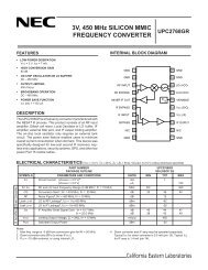
AN1020 Active Mixer Design Using the NE25139 Dual Gate MESFET
AN1020 Active Mixer Design Using the NE25139 Dual Gate MESFET
AN1020 Active Mixer Design Using the NE25139 Dual Gate MESFET

Create successful ePaper yourself
Turn your PDF publications into a flip-book with our unique Google optimized e-Paper software.
California Eastern Laboratories<br />
<strong>AN1020</strong><br />
<strong>Active</strong> <strong>Mixer</strong> <strong>Design</strong> <strong>Using</strong> <strong>the</strong> <strong>NE25139</strong><br />
<strong>Dual</strong> <strong>Gate</strong> <strong>MESFET</strong><br />
APPLICATION NOTE<br />
Introduction<br />
This application note documents <strong>the</strong> design method and<br />
results of using <strong>the</strong> <strong>NE25139</strong> as an active mixer for <strong>the</strong> ISM<br />
band of 902-928 MHz. The IF frequency will be 70 MHz, and<br />
<strong>the</strong> LO frequency range will be 832-858 MHz. The design<br />
goals for this mixer are to have a conversion gain of at least 11<br />
dB, and a noise figure lower than 7 dB while keeping <strong>the</strong> costs<br />
as low as possible. The <strong>NE25139</strong> could be used as a mixer in<br />
ISM band spread spectrum radios, cellular telephones, or any<br />
UHF applications.<br />
<strong>Design</strong> Philosophy and Method<br />
The challenge to every receiver designer is to have a front end<br />
that is sensitive and at <strong>the</strong> same time robust in a multiple signal<br />
environment. Excessive gain before <strong>the</strong> IF filtering can make<br />
<strong>the</strong> receiver sensitive, but at <strong>the</strong> same time very vulnerable to<br />
saturation and intermodulation by unwanted signals. The<br />
trick is to have adequate gain to set <strong>the</strong> noise figure but not<br />
excessive gain.<br />
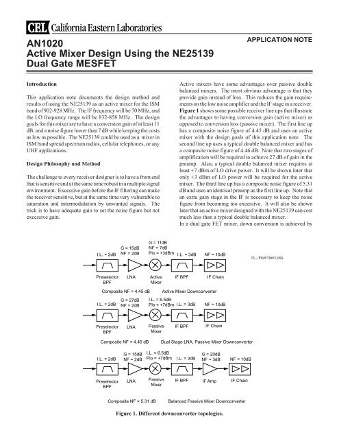
<strong>Active</strong> mixers have some advantages over passive double<br />
balanced mixers. The most obvious advantage is that <strong>the</strong>y<br />
provide gain instead of loss. This reduces <strong>the</strong> gain requirements<br />
on <strong>the</strong> low noise amplifier and <strong>the</strong> IF stage in a receiver.<br />
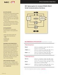
Figure 1 shows some possible receiver line ups that illustrate<br />
<strong>the</strong> advantages to having conversion gain (active mixer) as<br />
opposed to conversion loss (passive mixer). The first line up<br />
has a composite noise figure of 4.45 dB and uses an active<br />
mixer with <strong>the</strong> design goals of this application note. The<br />
second line up uses a typical double balanced mixer and has<br />
a composite noise figure of 4.46 dB. Note that two stages of<br />
amplification will be required to achieve 27 dB of gain in <strong>the</strong><br />
preamp. Also, a typical double balanced mixer requires at<br />
least +7 dBm of LO drive power. It will be shown later that<br />
only +3 dBm of LO power will be required for <strong>the</strong> active<br />
mixer. The third line up has a composite noise figure of 5.31<br />
dB and uses an identical preamp as <strong>the</strong> first line up. Note that<br />
an extra gain stage in <strong>the</strong> IF is necessary to keep <strong>the</strong> noise<br />
figure from becoming too excessive. It will also be shown<br />
later that an active mixer designed with <strong>the</strong> <strong>NE25139</strong> can cost<br />
much less than a typical double balanced mixer.<br />
In a dual gate FET mixer, down conversion is achieved by<br />
I.L. = 2dB<br />
G = 15dB<br />
NF = 2dB<br />
G = 11dB<br />
NF = 7dB<br />
Plo = +3dBm<br />
I.L. = 3dB<br />
NF = 10dB<br />
I.L.: Insertion Loss<br />
Preselector<br />
BPF<br />
LNA<br />
<strong>Active</strong><br />
<strong>Mixer</strong><br />
IF BPF<br />
IF Chain<br />
Composite NF = 4.45 dB<br />
I.L. = 2dB<br />
G = 27dB<br />
NF = 2dB<br />
I.L. = 6.5dB<br />
Plo = +7dBm<br />
<strong>Active</strong> <strong>Mixer</strong> Downconverter<br />
I.L. = 3dB<br />
NF = 10dB<br />
Preselector<br />
BPF<br />
LNA<br />
Passive<br />
<strong>Mixer</strong><br />
IF BPF<br />
IF Chain<br />
Composite NF = 4.45 dB<br />
<strong>Dual</strong> Stage LNA, Passive <strong>Mixer</strong> Downconverter<br />
I.L. = 2dB<br />
G = 15dB<br />
NF = 2dB<br />
I.L. = 6.5dB<br />
Plo = +7dBm<br />
I.L. = 3dB<br />
G = 20dB<br />
NF = 3dB<br />
NF = 10dB<br />
Preselector<br />
BPF<br />
LNA<br />
Passive<br />
<strong>Mixer</strong><br />
IF BPF<br />
IF Amp<br />
IF Chain<br />
Composite NF = 5.31 dB<br />
Balanced Passive <strong>Mixer</strong> Downconverter<br />
Figure 1. Different downconverter topologies.
<strong>AN1020</strong><br />
varying <strong>the</strong> transconductance with a local oscillator signal on<br />
one gate and applying <strong>the</strong> RF signal to <strong>the</strong> o<strong>the</strong>r gate. The IF<br />
signal is <strong>the</strong>n extracted from <strong>the</strong> drain.<br />
<strong>Design</strong>ing a mixer with <strong>the</strong> <strong>NE25139</strong> boils down to an<br />
impedance matching problem. The RF gate should be conjugately<br />
matched at <strong>the</strong> RF frequency and see a short circuit at<br />
<strong>the</strong> IF frequency. The LO gate should be conjugately matched<br />
at <strong>the</strong> LO frequency and short circuited at <strong>the</strong> IF frequency.<br />
Shorting <strong>the</strong> gates at <strong>the</strong> IF frequency helps prevent amplification<br />
of noise that would fall into <strong>the</strong> IF passband, and hence,<br />
helps to lower <strong>the</strong> noise figure of <strong>the</strong> mixer. Shorting <strong>the</strong> gates<br />
at <strong>the</strong> IF frequency also increases <strong>the</strong> conversion gain. The<br />
drain should be conjugately matched at <strong>the</strong> IF frequency and<br />
short circuited at <strong>the</strong> RF and LO frequencies. According to<br />
Maas 1 short circuiting <strong>the</strong> drain at <strong>the</strong> RF and LO frequencies<br />
provides a stable termination over a broad range of frequencies<br />
and provides for optimum gain and noise figure at <strong>the</strong> IF<br />
frequency. Ano<strong>the</strong>r important advantage is that it helps<br />
attenuate LO feed through into <strong>the</strong> IF output.<br />
Impedance Matching <strong>the</strong> <strong>NE25139</strong><br />
Although a mixer is a nonlinear circuit <strong>the</strong> linear S-parameters<br />
can be used as a starting point for <strong>the</strong> impedance matching<br />
task. Then with some intelligent, empirical optimization on<br />
<strong>the</strong> lab bench, <strong>the</strong> job can be finished. The S-parameters at <strong>the</strong><br />
IF, RF, and LO frequencies are shown in Table 1. (VDS = 5<br />
V, IDS = 10 mA, VGS 2 = 1V). Even though <strong>the</strong>se are not <strong>the</strong><br />
exact bias conditions that will be used, <strong>the</strong>se S-parameters<br />
will be close enough. The bias conditions that will be used in<br />
<strong>the</strong> actual design are VDS = 4.2V, IDS = 7.5 mA, VGS1 =<br />
VGS2 =-0.75 V.<br />
S-Parameter 70 MHz(IF) 845 MHz(LO) 915 MHz(RF)<br />
S 11<br />
0.99 < -3° 0.95 < -25° 0.94 < -29°<br />
S 21<br />
2.36 < 177° 2.23 < 142° 2.45 < 137°<br />
S 12<br />
0.001 < 87° 0.005 < 79° 0.005 < 79°<br />
S 22<br />
0.97 < -1° 0.96 < -9° 0.99 < -13°<br />
reflection coefficient, Γ o<br />
is <strong>the</strong> output reflection coefficient,<br />
and Γ S<br />
is <strong>the</strong> source reflection coefficient. Some assumptions<br />
must be made in order to make <strong>the</strong>se calculations. These<br />
assumptions are as follows: <strong>the</strong> drain is short circuited at <strong>the</strong><br />
RF and LO frequencies; <strong>the</strong> gates are well isolated from one<br />
ano<strong>the</strong>r, and <strong>the</strong> gates are short circuited at <strong>the</strong> IF frequency.<br />
The reason for <strong>the</strong> good isolation between <strong>the</strong> gates is that <strong>the</strong><br />
gate to gate capacitance is very low. Even though <strong>the</strong> S-<br />
parameters were measured with <strong>the</strong> transistor configured as a<br />
two port device, assuming that <strong>the</strong> impedance is equal at both<br />
of <strong>the</strong> gates is still a reasonable approximation. The main goal<br />
of <strong>the</strong> impedance matching calculations is to come up with a<br />
good topology that will be close and that can be optimized on<br />
<strong>the</strong> bench. Because <strong>the</strong> drain is short circuited at <strong>the</strong> RF and<br />
LO frequencies Γ L<br />
=-1 is used in <strong>the</strong> formulas for <strong>the</strong> RF and<br />
LO reflection coefficient calculations. Because <strong>the</strong> gates are<br />
short circuited at <strong>the</strong> IF frequency Γ S<br />
=-1 is used for <strong>the</strong> IF<br />
reflection coefficient calculations. Plugging <strong>the</strong> S-parameters<br />
and <strong>the</strong> source and load reflection coefficients into <strong>the</strong> formula<br />
gives<br />
Γ RF = 0.93 < -28.3°<br />
Γ LO = 0.95 < -24.7°<br />
Γ IF = 0.97 < -0.9°<br />
Now <strong>the</strong> formula from Gonzales 2<br />
Ζ = Ζ o [(1 + Γ) / (1 − Γ)]<br />
where Z o<br />
= 50 Ω, can be used to convert <strong>the</strong> reflection<br />
coefficients into impedances. The results of <strong>the</strong>se calculations<br />
are shown below:<br />
Ζ RF = 29.7 - j194 Ω<br />
Ζ LO = 26.5 - j225.4 Ω<br />
Ζ IF = 2,472 - j1,416 Ω<br />
where Z RF<br />
is <strong>the</strong> impedance looking into gate 2 at <strong>the</strong> RF<br />
frequency, Z LO<br />
is <strong>the</strong> impedance looking onto gate 1 at <strong>the</strong> LO<br />
frequency, and Z IF<br />
is <strong>the</strong> impedance looking into <strong>the</strong> drain at<br />
<strong>the</strong> IF frequency.<br />
The impedance matching topology and biasing circuitry are<br />
shown in Figure 2. Note that <strong>the</strong> source is bypassed at RF<br />
frequencies with <strong>the</strong> 47 pF capacitor and at IF frequencies<br />
with <strong>the</strong> 0.01 uF capacitor. This is critical for maintaining<br />
stability.<br />
Table 1. Linear S-parameters<br />
The impedance at each port of <strong>the</strong> mixer can be calculated<br />
using <strong>the</strong> formulas from Gonzalez 2<br />
and<br />
Γ o = S 22 + (S 12 S 21 Γ s ) / (1 - S 11 Γ s )<br />
Γ i = S 11 + (S 12 S 21 Γ L ) / (1 - S 22 Γ L )<br />
where Γ i<br />
is <strong>the</strong> input reflection coefficient, Γ L<br />
is <strong>the</strong> load
<strong>AN1020</strong><br />
LO<br />
C3<br />
47pF<br />
L1<br />
C1 22nH<br />
0.5pF G1<br />
D<br />
RF<br />
G2 S<br />
C2<br />
0.8pF<br />
L2<br />
R1<br />
18nH<br />
100Ω<br />
+5V<br />
Figure 2. Calculated Value Based on Small Signal<br />
S-parameters.<br />
It is best to have <strong>the</strong> source well bypassed for <strong>the</strong> broadest<br />
range of frequencies possible. The gates are matched to 50<br />
ohms with a shunt inductor and series capacitor. Note that <strong>the</strong><br />
shunt inductor will provide <strong>the</strong> desired short circuit at <strong>the</strong> IF<br />
frequency. The inductors at <strong>the</strong> gates also provide a DC<br />
ground to bias <strong>the</strong> transistor. R1 in <strong>the</strong> source sets <strong>the</strong> drain<br />
current to about 7.5 mA. R2 helps to isolate <strong>the</strong> mixer circuit<br />
from <strong>the</strong> power supply and very little voltage is dropped<br />
across it. The drain is matched to 50 ohms with a π circuit.<br />
<strong>Using</strong> a π topology lowers <strong>the</strong> Q of <strong>the</strong> matching and also<br />
serves as a low pass filter to attenuate LO feed through. C7<br />
provides <strong>the</strong> short circuit at <strong>the</strong> LO and RF frequencies.<br />
R2<br />
10Ω<br />
L3<br />
270nH<br />
Q1<br />
<strong>NE25139</strong><br />
C5<br />
47pF<br />
C4<br />
0.01uF<br />
C7<br />
47pF<br />
C6<br />
0.01uF<br />
L4<br />
270nH<br />
C8<br />
220pF<br />
IF<br />
well matched. Simply adjusting element values while monitoring<br />
<strong>the</strong> gain can be a frustrating and time consuming<br />
experience. Fortunately, all <strong>the</strong> ports are well isolated from<br />
one ano<strong>the</strong>r and can be independently matched one at a time.<br />
As soon as <strong>the</strong> ports are matched <strong>the</strong> gain will be achieved.<br />
Conjugately matching all <strong>the</strong> ports gives <strong>the</strong> best noise figure<br />
and gain. Figure 3 shows <strong>the</strong> final mixer circuit that has been<br />
empirically optimized. When first measured <strong>the</strong> return loss<br />
notch at <strong>the</strong> LO gate was 100 MHz too high and <strong>the</strong> return loss<br />
notch at <strong>the</strong> RF gate was 150 MHz too low. The return loss<br />
switch at <strong>the</strong> IF port was 40 Mhz too low. Air wound coils<br />
were used for L1 and L2. Optimization of <strong>the</strong> matching at <strong>the</strong><br />
gates was easily accomplished by knifing apart <strong>the</strong> windings<br />
or squeezing <strong>the</strong>m toge<strong>the</strong>r. Simply lowering <strong>the</strong> value of C8<br />
matched <strong>the</strong> impedance at <strong>the</strong> IF port. It was found that <strong>the</strong> best<br />
noise figure was achieved with IDS = 3.5 mA. At 915 MHz <strong>the</strong><br />
SSB noise figure was 5.4 dB and <strong>the</strong> gain was 11.7 dB. The<br />
conversion gain return loss and noise figure at <strong>the</strong> RF port are<br />
graphed in Figure 4. The return loss at <strong>the</strong> IF port was 22 dB.<br />
With P LO<br />
= +3 dBm, <strong>the</strong> P1dB was measured to be -1 dBm, and<br />
<strong>the</strong> IP3 OUT<br />
was measured to be +7.5 dBm. The LO to RF<br />
isolation is 21 dB and <strong>the</strong> LO to IF isolation is 31 dB.<br />
If an even higher P1dB and IP3 are desired, it can be achieved<br />
by optimizing <strong>the</strong> circuit for best P1dB and IP3. A much<br />
higher IP3 can be achieved by increasing <strong>the</strong> drain current;<br />
however, an increase in noise figure will result.<br />
Now that <strong>the</strong> initial calculations have been completed, <strong>the</strong><br />
circuit must be optimized on <strong>the</strong> lab bench. The input impedance<br />
on both of <strong>the</strong> gates is somewhat dependent on <strong>the</strong><br />
amount of LO power used. If <strong>the</strong> FET is biased at IDS = 7.5<br />
mA, about +3 dBm of LO power is a good place to start. <strong>Using</strong><br />
a network analyzer you can quickly see how close <strong>the</strong> impedance<br />
match is by monitoring <strong>the</strong> return loss at each of <strong>the</strong> ports.<br />
A deep notch in <strong>the</strong> return loss should occur at <strong>the</strong> center<br />
frequency for each of <strong>the</strong> ports. When matching <strong>the</strong> RF and IF<br />
ports, be sure to have +3 dBm of LO power pumping <strong>the</strong> LO<br />
gate. Also, be sure <strong>the</strong> network analyzer output power is low<br />
enough to ensure small signal measurements at <strong>the</strong> RF and IF<br />
ports, and that <strong>the</strong> output power of <strong>the</strong> network analyzer is set<br />
close to +3 dBm when measuring <strong>the</strong> return loss at <strong>the</strong> LO port.<br />
Although <strong>the</strong> ports are well isolated from each o<strong>the</strong>r, <strong>the</strong> LO<br />
drive affects <strong>the</strong> biasing and hence <strong>the</strong> impedance at all <strong>the</strong><br />
ports. While adjusting <strong>the</strong> impedance matching values at each<br />
port watch <strong>the</strong> effect each change has on <strong>the</strong> return loss notch.<br />
In this manner, <strong>the</strong> notch can be moved to center frequency<br />
and a good match will be achieved. If a network analyzer is not<br />
available, a tracking generator, spectrum analyzer, and a<br />
directional coupler can be used to monitor <strong>the</strong> return loss as <strong>the</strong><br />
elements are adjusted. It is highly recommended that this<br />
circuit be optimized by first making sure that all <strong>the</strong> ports are<br />
LO<br />
L1<br />
5 turns, 28 AWG<br />
.050 I.D<br />
Ċ1<br />
0.5pF<br />
RF<br />
C2<br />
0.5pF<br />
L2<br />
5 turns, 28 AWG<br />
.050 I.D.<br />
C3<br />
47pF<br />
G1<br />
G2<br />
R1<br />
270Ω<br />
+5V<br />
Figure 3. Optimized Value for Best Noise Figure.<br />
R2<br />
10Ω<br />
L3<br />
270nH<br />
D Q1<br />
<strong>NE25139</strong><br />
S<br />
C5<br />
47pF<br />
C4<br />
0.01uF<br />
C7<br />
42pF<br />
L4<br />
270nH<br />
C8<br />
82pF<br />
C8<br />
0.01uF<br />
IF
<strong>AN1020</strong><br />
Gain and Noise Figure (dB)<br />
13<br />
0<br />
Gain<br />
10<br />
-10<br />
7<br />
Noise Figure<br />
4<br />
-20<br />
902 915 928<br />
Return Loss (dB)<br />
(RF POUT)<br />
Gain and Noise Figure (dB)<br />
13<br />
0<br />
Noise Figure<br />
10<br />
7<br />
Gain<br />
-10<br />
-20<br />
902 915 928<br />
Return Loss (dB)<br />
(RF POUT)<br />
Frequency (MHz)<br />
Frequency (MHz)<br />
Figure 4. <strong>Mixer</strong> with Best Noise Figure<br />
A second mixer circuit was optimized on <strong>the</strong> bench for best<br />
P1dB and IP3. The bias point was changed to <strong>the</strong> original 7.5<br />
mA. The matching elements on <strong>the</strong> gates were empirically<br />
modified while monitoring <strong>the</strong> P1dB and IP3 performance.<br />
Figure 5 shows <strong>the</strong> optimized values for <strong>the</strong> higher linearity<br />
mixer. With P LO<br />
= +3 dBm, <strong>the</strong> P1dB was measured to be +4<br />
dBm, and <strong>the</strong> IP3 OUT<br />
was measured to be +15 dBm. At 915<br />
MHz <strong>the</strong> SSB noise figure was 11 dB and <strong>the</strong> gain was 10.7<br />
dB. The conversion gain, <strong>the</strong> return loss and <strong>the</strong> noise figure<br />
are graphed in Figure 6. The return loss at <strong>the</strong> IF port was 24<br />
dB. The LO to RF isolation is 46 dB and <strong>the</strong> LO to IF isolation<br />
is 16 dB and <strong>the</strong> LO to IF isolation is 24 dB.<br />
The input and ouput impedances of <strong>the</strong> <strong>NE25139</strong> are very<br />
high. This makes <strong>the</strong> matching a little bit touchy and narrow<br />
band. In narrow band receivers (e.g., <strong>the</strong> RF bandwidth is less<br />
than 50 MHz) this can be advantageous. Both of <strong>the</strong> circuits<br />
Figure 6. <strong>Mixer</strong> with Best Linearity<br />
in Figures 3 and 5 had -5 dB of conversion gain at <strong>the</strong> image<br />
frequency. This provides 16.7 dB of image rejection for <strong>the</strong><br />
circuit in Figure 3 and 15.7 dB of image rejection for <strong>the</strong><br />
circuit in Figure 5. The image rejection performance of a<br />
receiver could be improved by as much as 16.7 dB without<br />
adding any cost to <strong>the</strong> preselector filter. Or <strong>the</strong> requirements<br />
on <strong>the</strong> preselector filter could be relaxed to provide fur<strong>the</strong>r<br />
cost saving. To ensure consistent performance yield in production,<br />
<strong>the</strong> air wound coils should be adjusted while monitoring<br />
<strong>the</strong> gain somewhere in <strong>the</strong> IF stage with an oscilloscope.<br />
The local oscillator power was varied +/- 3 dB on both<br />
versions of <strong>the</strong> mixer and <strong>the</strong> effects this had on conversion<br />
gain and noise figure are shown in Tables 2 and 3 below.<br />
LO<br />
L1<br />
3 turns, 28 AWG<br />
.050 I.D.<br />
C1<br />
1pF<br />
RF<br />
C2<br />
0.5pF<br />
L2<br />
4 turns, 28 AWG<br />
.050 I.D.<br />
C3<br />
47pF<br />
G1<br />
G2<br />
R1<br />
100Ω<br />
+5V<br />
R2<br />
10Ω<br />
C4<br />
Figure 5. Optimized Value for Best Linearity<br />
L3<br />
270nH<br />
D Q1<br />
<strong>NE25139</strong><br />
S<br />
C5<br />
47pF<br />
0.01uF<br />
C7<br />
42pF<br />
L4<br />
270nH<br />
C8<br />
82pF<br />
C8<br />
0.01uF<br />
IF<br />
P LO<br />
Gain NF<br />
0 dBm 11.6 dB 5.9 dB<br />
3 dBm 11.7 dB 5.4 dB<br />
6 dBm 11.8 dB 5.0 dB<br />
Table 2. Best Noise Figure Circuit<br />
P LO<br />
Gain NF<br />
0 dBm 10.5 dB 12 dB<br />
3 dBm 10.7 dB 11 dB<br />
6 dBm 10.9 dB 10.5 dB<br />
Table 3. Best Linearity Circuit<br />
As can be seen <strong>the</strong> mixer performance was not critically<br />
affected by small changes in <strong>the</strong> LO power. This should make<br />
<strong>the</strong> variations in LO power that can occur in production noncritical.
<strong>AN1020</strong><br />
The <strong>NE25139</strong> is available in several IDSS ranges. The U73<br />
range was used for this circuit (IDSS = 20 - 30 mA). The higher<br />
IDSS range devices will give better third order intercept point<br />
performance. If <strong>the</strong> U74 range were to be used even better<br />
third order intercept point performance can be expected. It is<br />
highly recommended that at least <strong>the</strong> U73 range device be<br />
used when designing a mixer.<br />
Table 4 shows <strong>the</strong> parts list for <strong>the</strong> circuit in Figure 3 (best<br />
noise figure circuit) and <strong>the</strong> cost of <strong>the</strong> parts in 100K quantities.<br />
Reference Description Cost*<br />
<strong>Design</strong>ator<br />
Q1 <strong>NE25139</strong>T1U73 <strong>Dual</strong> 0.76<br />
<strong>Gate</strong> <strong>MESFET</strong><br />
C1, C2 0.5 PF, NPO CAP, 0805, 0.045<br />
+/- 0.1PF<br />
C4, C6 0.01 UF, CAP, 0805, 0.015<br />
+/- 10%<br />
C3, C5 47 PF, NPO CAP, 0805, 0.015<br />
+/- 5%<br />
C7 42 PF, NPO CAP, 0805, 0.015<br />
+/- 5%<br />
C8 82 PF, NPO CAP, 0805, 0.015<br />
+/- 5%<br />
R2 10 Ohm, Resistor, 0805, 0.005<br />
+/- 10%<br />
R1 270 Ohm, Resistor, 0805, 0.005<br />
+/- 10%<br />
L1, L2 270 NH, Inductor, 0805, 0.13<br />
+/- 10%<br />
L3, L4 Air Wound Coil, 5 turns, 0.05<br />
26 AWG, 0.050 Inch Inner<br />
Diameter<br />
Total Cost of <strong>Mixer</strong> in 100K Quantities 1.31<br />
Conclusion<br />
This application note presents <strong>the</strong> results of using <strong>NE25139</strong> as<br />
an active mixer. It has been shown that simple impedance<br />
matching methods and empirical optimization can be used to<br />
design a high performance active mixer. A mixer that only<br />
uses 3.5 mA of current and +3 dBm of LO power was<br />
designed. The noise figure was 5.4 dB and <strong>the</strong> conversion gain<br />
was 11.7 dB. The output third order intercept point was +7.5<br />
dBm. Because this mixer only uses 3.5 mA of current it would<br />
be ideal for battery operated receivers. Fur<strong>the</strong>r current savings<br />
can also be obtained when using <strong>the</strong> <strong>NE25139</strong> as an active<br />
mixer because fewer gain stages in <strong>the</strong> LNA or IF are required.<br />
It was also shown that higher IP3 performance could be<br />
achieved by increasing <strong>the</strong> drain current but a trade off in<br />
increased noise figure would result. By using <strong>the</strong> <strong>NE25139</strong> as<br />
a discrete active mixer, <strong>the</strong> designer can optimize its performance<br />
to suit <strong>the</strong> application. There are many o<strong>the</strong>r topologies<br />
that could be used with <strong>the</strong> <strong>NE25139</strong> to accomplish <strong>the</strong><br />
impedance matching, providing <strong>the</strong> proper short circuits and<br />
conjugate matches are achieved. Cost savings and some<br />
performance advantages can be achieved by using <strong>the</strong> <strong>NE25139</strong><br />
instead of <strong>the</strong> standard passive double balanced mixers that<br />
are used in many designs.<br />
References<br />
1. Maas, S., Microwave <strong>Mixer</strong>s, 2nd Ed. Artech House,<br />
1993, pg. 315<br />
2. Gonzalez, G., Microwave Transistor Amplifiers,<br />
Prentice-Hall, 1984, pg. 6 & 85.<br />
Table 4. Best Noise Figure Circuit Parts List<br />
* The cost reflected in this table is an estimate based on<br />
information available as of <strong>the</strong> date of publication. For <strong>the</strong><br />
latest prices, contact California Eastern Laboratories.<br />
The total parts cost for 100K quantities in production is only<br />
$1.31 for <strong>the</strong> mixer circuit. <strong>Using</strong> <strong>the</strong> <strong>NE25139</strong> as an active<br />
mixer relaxes <strong>the</strong> gain requirements in <strong>the</strong> LNA and <strong>the</strong> IF<br />
stage to achieve a given receiver sensitivity. The requirements<br />
on <strong>the</strong> preselector filter to achieve a given image rejection can<br />
also be relaxed. These two advantages should result in fur<strong>the</strong>r<br />
cost savings.<br />
California Eastern Laboratories<br />
Exclusive Agents for NEC RF, Microwave and Optoelectronic<br />
semiconductor products in <strong>the</strong> U.S. and Canada<br />
4590 Patrick Henry Drive, Santa Clara, CA 95054-1817<br />
Telephone 408-988-3500 • FAX 408-988-0279 •Telex 34/6393<br />
Internet: http:/WWW.CEL.COM<br />
Information and data presented here is subject to change without notice.<br />
California Eastern Laboratories assumes no responsibility for <strong>the</strong> use of<br />
any circuits described herein and makes no representations or warranties,<br />
expressed or implied, that such circuits are free from patent infingement.<br />
© California Eastern Laboratories 02/04/2003