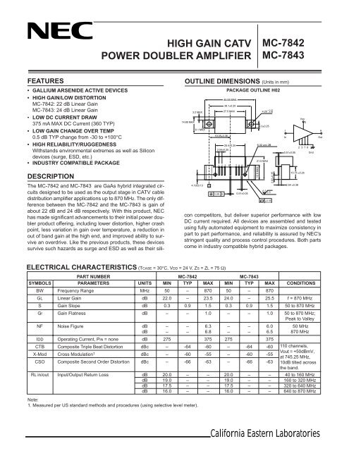
high gain catv power doubler amplifier mc-7842 mc-7843
high gain catv power doubler amplifier mc-7842 mc-7843
high gain catv power doubler amplifier mc-7842 mc-7843

You also want an ePaper? Increase the reach of your titles
YUMPU automatically turns print PDFs into web optimized ePapers that Google loves.
2.62±0.35HIGH GAIN CATVPOWER DOUBLER AMPLIFIERMC-<strong>7842</strong>MC-<strong>7843</strong>FEATURES• GALLIUM ARSENIDE ACTIVE DEVICES• HIGH GAIN/LOW DISTORTIONMC-<strong>7842</strong>: 22 dB Linear GainMC-<strong>7843</strong>: 24 dB Linear Gain• LOW DC CURRENT DRAW375 mA MAX DC Current (360 TYP)• LOW GAIN CHANGE OVER TEMP0.5 dB TYP change from -30 to +100°C• HIGH RELIABILITY/RUGGEDNESSWithstands environmental extremes as well as Silicondevices (surge, ESD, etc.)• INDUSTRY COMPATIBLE PACKAGEDESCRIPTIONOUTLINE DIMENSIONS (Units in mm)4.19±0.1325.4±0.252.54±0.25PACKAGE OUTLINE H023.2 MAX27.5 MAX4.25 + - 0.350.2514.85 MAX4.0±0.258.1 MAX A19.05±0.3845.08 MAX38.1±0.251 2 3 5 7 8 90.38.. A0.51±0.0521.5 MAXVDD5The MC-<strong>7842</strong> and MC-<strong>7843</strong> are GaAs hybrid integrated circuitsdesigned to be used as the output stage in CATV cabledistribution <strong>amplifier</strong> applications up to 870 MHz. The only differencebetween the MC-<strong>7842</strong> and the MC-<strong>7843</strong> is <strong>gain</strong> ofabout 22 dB and 24 dB respectively. With this product, NEChas made significant advancements to their initial <strong>power</strong> <strong>doubler</strong>product offering, including lower distortion, <strong>high</strong>er crashpoint, less variation in <strong>gain</strong> over temperature, a reduction inout of band <strong>gain</strong> at the <strong>high</strong> end, and improved ability to survivean overdrive. Like the previous products, these devicessurvive such hazards as surge and ESD as well as their siliconcompetitors, but deliver superior performance with lowDC current required. All devices are assembled and testedusing fully automated equipment to maximize consistency inpart to part performance, and reliability is assured by NEC'sstringent quality and process control procedures. Both partscome in industry compatible hybrid packages.12.9 MAX6-32 unc 2B6.32.5±0.05 1In0.51±0.052.54 ±0.382 3 7 810.75 ±0.25Gnd9OutELECTRICAL CHARACTERISTICS (TCASE = 30°C, VDD = 24 V, ZS = ZL = 75 Ω)PART NUMBER MC-<strong>7842</strong> MC-<strong>7843</strong>SYMBOLS PARAMETERS UNITS MIN TYP MAX MIN TYP MAX CONDITIONSBW Frequency Range MHz 50 – 870 50 – 870GL Linear Gain dB 22.0 – 23.5 24.0 – 25.5 f = 870 MHzS Gain Slope dB 0.3 0.9 1.5 0.3 0.9 1.5 50 to 870 MHzGf Gain Flatness dB – – 1.0 – – 1.0 50 to 870 MHz;Peak to ValleyNF Noise Figure dB – – 6.3 – – 6.0 50 MHzdB – – 6.8 – – 6.5 870 MHzIDD Operating Current, PIN = none dB 275 375 275 375CTB Composite Triple Beat Distortion dBc – -64 -60 – -64 -60X-Mod Cross Modulation 1 dBc – -60 -55 – -60 -55CSO Composite Second Order Distortion dBc – -66 -63 – -66 -63RL in/out Input/Output Return Loss dB 20.0 – – 20.0 – – 40 to 160 MHzdB 19.0 – – 19.0 – – 160 to 320 MHzdB 17.5 – – 17.5 – – 320 to 640 MHzdB 16.0 – – 16.0 – – 640 to 870 MHzNote:1. Measured per US standard methods and procedures (using selective level meter).110 channels,Vout = +50dBmV,at 745.25 MHz,10dB tilted acrossthe band.California Eastern Laboratories
MC-<strong>7842</strong>, MC-<strong>7843</strong>ABSOLUTE MAXIMUM RATINGS 1 (TCASE= 30 °C)SYMBOLS PARAMETERS UNITS RATINGSVDD Supply Voltage V 30Vi Input Voltage 2 dBmV 65TC Operating Case Temperature °C -30 to +100TSTG Storage Temperature °C -40 to +100Note:1. Operation in excess of any one of these parameters may resultin permanent damage.2. Maximum single channel <strong>power</strong> applied to the input for 1 minutewith no measurable degradation in performance.RECOMMENDED OPERATING CONDITIONS(ZS= ZL= 75Ω)SYMBOLS PARAMETERS UNITS MIN TYP MAXVDD Supply Voltage V 23.5 24.0 24.5Vi Input Voltage 1MC-<strong>7842</strong> dBmV – 27.0 31.5MC-<strong>7843</strong> dBmV – 25.0 29.5TC Operating Case °C -30 +25 +85TemperatureNote:1. Test Condition: 110 channels, 10 dB tilted across the band.NOTES ON CORRECT USE1. The space between PC board and root of the lead should bekept more than 1 mm to prevent undesired stress on the lead andalso should be kept less than 4 mm to prevent undesired parasiticinductance.Recommended space is 2.0 to 3.0 mm typical.2. Recommended torque strength of the screw is 59 to 78 Ncm.3. Form the ground pattern as wide as possible to minimize groundimpedance. (to prevent undesired oscillation)All the ground pins must be connected together with wide groundpattern to decrease impedance difference.RECOMMENDED SOLDERING CONDITIONSThis product should be soldered in the following recommendedconditions. Other soldering methods and conditions than therecommended conditions are to be consulted with our salesrepresentatives.Soldering Soldering ConditionMethod Conditions SymbolPin Part Heating Pin area temperature: less –than 260°C 1Hour: Within 2 sec./pinNote.1. The point of pin part heating must be kept at a distance of morethan 1.2 mm from the root of lead.Life Support ApplicationsThese NEC products are not intended for use in life support devices, appliances, or systems where the malfunction of these products can reasonablybe expected to result in personal injury. The customers of CEL using or selling these products for use in such applications do so at their own risk andagree to fully indemnify CEL for all damages resulting from such improper use or sale.EXCLUSIVE NORTH AMERICAN AGENT FOR RF, MICROWAVE & OPTOELECTRONIC SEMICONDUCTORSCALIFORNIA EASTERN LABORATORIES • Headquarters • 4590 Patrick Henry Drive • Santa Clara, CA 95054-1817 • (408) 988-3500 • Telex 34-6393 • FAX (408) 988-027924-Hour Fax-On-Demand: 800-390-3232 (U.S. and Canada only) • Internet: http://WWW.CEL.COMDATA SUBJECT TO CHANGE WITHOUT NOTICE 07/10/2002