Replica molding with a polysiloxane mold provides this ... - EPFL
Replica molding with a polysiloxane mold provides this ... - EPFL
Replica molding with a polysiloxane mold provides this ... - EPFL

You also want an ePaper? Increase the reach of your titles
YUMPU automatically turns print PDFs into web optimized ePapers that Google loves.
REVIEWS<br />
G. M. Whitesides et al.<br />
<strong>with</strong> photolithography. Figure 28 shows SEM images of some<br />
patterned microstructures that were fabricated by MIMIC<br />
from systems involving solvents or suspending liquids. The<br />
ability to form patterned microstructures offers new opportunities<br />
for these materials. For example, the closely packed,<br />
multilayered structures of polymer beads are interesting for<br />
potential applications in chromatography and diffractive<br />
optics. [192] The ability to form patterned microstructures of<br />
conducting polymers <strong>provides</strong> a potential route to flexible, allplastic<br />
electronic and optoelectronic devices. [193]<br />
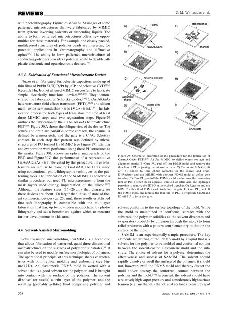
4.3.4. Fabrication of Functional Microelectronic Devices<br />
Nuzzo et al. fabricated ferroelectric capacitors made up of<br />
thin films of Pt/Pb(Zr,Ti)O 3 /Pt by mCP and selective CVD. [194]<br />
Recently Hu, Jeon et al. used MIMIC successfully to fabricate<br />
simple, electrically functional devices. [195±197] They demonstrated<br />
the fabrication of Schottky diodes, [195] GaAs/AlGaAs<br />
heterostructure field effect transistors (FETs), [196] and silicon<br />
metal oxide semiconductor FETs (MOSFETs). [197] The fabrication<br />
process for both types of transistors required at least<br />
three MIMIC steps and two registration steps. Figure 29<br />
outlines the fabrication of the GaAs/AlGaAs heterostructure<br />
FET. [196] Figure 30 A shows the oblique view of the device. The<br />
source and drain are AuNiGe ohmic contacts, the channel is<br />
defined by a mesa etch, and the gate is a Cr/Au Schottky<br />
contact. In each step the pattern was defined by microstructures<br />
of PU formed by MIMIC (see Figure 29): Etching<br />
and evaporation were performed using these PU structures as<br />
the masks. Figure 30 B shows an optical micrograph of the<br />
FET, and Figure 30 C the performance of a representative<br />
GaAs/AlGaAs FET fabricated by <strong>this</strong> procedure. Its characteristics<br />
are similar to those of GaAs/AlGaAs FETs made<br />
using conventional photolithographic techniques as the patterning<br />
tools. The fabrication of the Si MOSFETs followed a<br />
similar procedure, but used PU microstructures to form the<br />
mask layers used during implantation of the silicon. [197]<br />
Although the feature sizes (16 ± 26 mm) that characterize<br />
these devices are about 100 larger than those of state-of-theart<br />
commercial devices (ca. 250 nm), these results established<br />
that soft lithography is compatible <strong>with</strong> the multilayer<br />
fabrication that has, up to now, been monopolized by photolithography<br />
and set a benchmark against which to measure<br />
further developments in <strong>this</strong> area.<br />
4.4. Solvent-Assisted Micro<strong><strong>mold</strong>ing</strong><br />
Solvent-assisted micro<strong><strong>mold</strong>ing</strong> (SAMIM) is a technique<br />
that allows fabrication of patterned, quasi-three-dimensional<br />
microstructures on the surfaces of polymeric substrates. [38] It<br />
can also be used to modify surface morphologies of polymers.<br />
The operational principle of <strong>this</strong> technique shares characteristics<br />
<strong>with</strong> both replica <strong><strong>mold</strong>ing</strong> and embossing (see Figure<br />
17 D). An elastomeric PDMS <strong>mold</strong> is wetted <strong>with</strong> a<br />
solvent that is a good solvent for the polymer, and is brought<br />
into contact <strong>with</strong> the surface of the polymer. The solvent<br />
dissolves (or swells) a thin layer of the polymer, and the<br />
resulting (probably gellike) fluid comprising polymer and<br />
Figure 29. Schematic illustration of the procedure for the fabrication of<br />
GaAs/AlGaAs FETs. [196] A) Use MIMIC to define ohmic contacts and<br />
alignment marks. B) Cure PU, peel off the PDMS <strong>mold</strong>, and remove the<br />
thin film of PU adjoining the microstructures. C) Evaporate AuNiGe, lift<br />
off PU, anneal to form ohmic contacts for the source, and drain.<br />
D) Register and use MIMIC <strong>with</strong> another PDMS <strong>mold</strong> to define etch<br />
trenches. E) Cure PU, peel off the PDMS <strong>mold</strong>, and remove the connecting<br />
film of PU. F) Etch in an aqueous solution of citric acid and hydrogen<br />
peroxide to remove the 2DEG in the etched trenches. G) Register and use<br />
MIMIC <strong>with</strong> a third PDMS <strong>mold</strong> to define the gate. H) Cure PU, peel off<br />
the PDMS <strong>mold</strong>, and remove the thin film of PU. I) Evaporate Cr/Au and<br />
lift off PU to form the gate.<br />
solvent conforms to the surface topology of the <strong>mold</strong>. While<br />
the <strong>mold</strong> is maintained in conformal contact <strong>with</strong> the<br />
substrate, the polymer solidifies as the solvent dissipates and<br />
evaporates (probably by diffusion through the <strong>mold</strong>) to form<br />
relief structures <strong>with</strong> a pattern complementary to that on the<br />
surface of the <strong>mold</strong>.<br />
SAMIM is an experimentally simple procedure. The key<br />
elements are wetting of the PDMS <strong>mold</strong> by a liquid that is a<br />
solvent for the polymer to be <strong>mold</strong>ed and conformal contact<br />
between the solvent-coated elastomeric <strong>mold</strong> and the substrate.<br />
The choice of solvent for a polymer determines the<br />
effectiveness and success of SAMIM. The solvent should<br />
rapidly dissolve or swell the surface of the polymer; it should<br />
not, however, swell the PDMS <strong>mold</strong> and thereby distort the<br />
<strong>mold</strong> and/or destroy the conformal contact between the<br />
polymer and the <strong>mold</strong>. [126] In general, the solvent should have<br />
a relatively high vapor pressure and a moderately high surface<br />
tension (e.g., methanol, ethanol, and acetone) to ensure rapid<br />
568 Angew. Chem. Int. Ed. 1998, 37, 550 ± 575