Replica molding with a polysiloxane mold provides this ... - EPFL
Replica molding with a polysiloxane mold provides this ... - EPFL
Replica molding with a polysiloxane mold provides this ... - EPFL

You also want an ePaper? Increase the reach of your titles
YUMPU automatically turns print PDFs into web optimized ePapers that Google loves.
REVIEWS<br />
contact printing will be discussed in <strong>this</strong> review since it is the<br />
one that seems to offer the most interesting combination of<br />
convenience and new capability.<br />
2.3. Contact Printing, <strong>Replica</strong> Molding, and Embossing<br />
Contact printing is an efficient method for pattern transfer.<br />
[105] A conformal contact between the stamp and the<br />
surface of the substrate is the key to its success. Printing has<br />
the advantage of simplicity and convenience: Once the stamp<br />
is available, multiple copies of the pattern can be produced<br />
using straightforward experimental techniques. Printing is an<br />
additive process; the waste of material is minimized. Printing<br />
also has the potential to be used for patterning large areas.<br />
Although contact printing is most suitable for two-dimensional<br />
fabrication, it has also been used to generate quasithree-dimensional<br />
structures through combination <strong>with</strong> other<br />
processes such as metal plating. [106]<br />
<strong>Replica</strong> <strong><strong>mold</strong>ing</strong> duplicates the informationÐfor example,<br />
the shape, the morphology, and the structureÐpresent in a<br />
master. It is a procedure that accommodates a wider range of<br />
materials than does photolithography. It also allows duplication<br />
of three-dimensional topologies in a single step, whereas<br />
photolithography is not able to replicate such structures. It has<br />
been used for the mass production of surface relief structures<br />
such as diffraction gratings, [107] holograms, [108] compact disks<br />
(CDs), [19, 20] and microtools. [109] <strong>Replica</strong> <strong><strong>mold</strong>ing</strong> <strong>with</strong> an<br />
appropriate material (usually in the form of a precursor)<br />
enables highly complex structures in the master to be<br />
faithfully duplicated into multiple copies <strong>with</strong> nanometer<br />
resolution in a reliable, simple, and inexpensive way. [110±112]<br />
The fidelity of replica <strong><strong>mold</strong>ing</strong> is determined by van der Waals<br />
interactions, wetting, and kinetic factors such as filling of the<br />
<strong>mold</strong>. These physical interactions should allow more accurate<br />
replication of features that are smaller than 100 nm than does<br />
photolithography, which is limited by optical diffraction. [10]<br />
Embossing is another cost-effective, high-throughput manufacturing<br />
technique that imprints microstructures in thermoplastic<br />
materials. [17, 18] The manufacturing of CDs based on<br />
imprinting in polycarbonate <strong>with</strong> nickel masters [17a] and of<br />
holograms by imprinting in SURPHEX photopolymer (Du-<br />
Pont) <strong>with</strong> fused quartz masters [17f] are two typical examples<br />
of large-volume commercial applications of <strong>this</strong> technique.<br />
Until recently embossing had not been seriously developed as<br />
a method for fabricating and manufacturing structures of<br />
semiconductors, metals, and other materials used in microelectronic<br />
circuitry. The beautiful work by Chou et al. showed<br />
that embossing can be used to make features as small as 25 nm<br />
in silicon, and has attracted attention to the potential of <strong>this</strong><br />
kind of patterning technique. [18]<br />
We are extending the capability of these patterning<br />
techniques by bringing new approaches and new materials<br />
into these areas. In particular, a combination of self-assembly<br />
(especially of self-assembled monolayers) and pattern transfer<br />
using elastomeric stamps, <strong>mold</strong>s, or masks constitutes the<br />
basis of soft lithographic methods. [33] It complements photolithography<br />
in a number of aspects and <strong>provides</strong> a wide range<br />
of new opportunities for micro- and nanofabrication.<br />
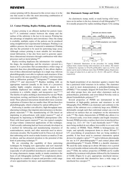
2.4. Elastomeric Stamps and Molds<br />
G. M. Whitesides et al.<br />
An elastomeric stamp, <strong>mold</strong>, or mask having relief structures<br />
on its surface is the key element of soft lithography. [33±38]<br />
It is usually prepared by replica <strong><strong>mold</strong>ing</strong> (Figure 5) by casting<br />
Figure 5. Schematic illustration of the procedure for casting PDMS<br />
replicas from a master having relief structures on its surface. The master<br />
is silanized by exposure to CF 3 (CF 2 ) 6 (CH 2 ) 2 SiCl 3 vapor (ca. 0.5 h); each<br />
master can be used to fabricate more than 50 PDMS replicas. Representative<br />
ranges of values for h, d, and l are 0.2 ± 20, 0.5 ± 200, and 0.5 ± 200 mm,<br />
respectively.<br />
the liquid prepolymer of an elastomer against a master that<br />
has a patterned relief structure in its surface. The elastomer<br />
we used in most demonstrations is poly(dimethylsiloxane)<br />
(PDMS), [113] for example, Sylgard 184 from Dow Corning. We<br />
and other groups have also used other elastomers such as<br />
polyurethanes, polyimides, and cross-linked Novolac resin (a<br />
[84, 85]<br />
phenol formaldehyde polymer).<br />
Several properties of PDMS are instrumental in the<br />
formation of high-quality patterns and structures in soft<br />
lithography. First, PDMS is an elastomer and conforms to the<br />
surface of the substrate over a relatively large area. PDMS is<br />
deformable enough such that conformal contact can even be<br />
achieved on surfaces that are nonplanar on the micrometer<br />
scale. [114] The elastic characteristic of PDMS also allows it to<br />
be released easily, even from complex and fragile structures.<br />
Second, PDMS <strong>provides</strong> a surface that is low in interfacial free<br />
energy (ca. 21.6 10 3 J m 2 ) and chemically inert: [113] Polymers<br />
being <strong>mold</strong>ed do not adhere irreversibly to or react <strong>with</strong><br />
the surface of PDMS. Third, PDMS is homogeneous, isotropic,<br />
and optically transparent down to about 300 nm: [115]<br />
UV cross-linking of prepolymers that are being <strong>mold</strong>ed is<br />
possible. It has been used to construct elastomeric optical<br />
devices for adaptive optics [116±119] and to fabricate photomasks<br />
for use in UV photolithography [120] and contact phase-shift<br />
photolithography. [121] Fourth, PDMS is a durable elastomer.<br />
We used the same stamp up to about 100 times over a period<br />
of several months <strong>with</strong>out noticeable degradation in performance.<br />
[85] Fifth, the surface properties of PDMS can be readily<br />
modified by treatment <strong>with</strong> plasma followed by the formation<br />
of SAMs (Figure 6) to give appropriate interfacial interactions<br />
<strong>with</strong> materials that themselves have a wide range of<br />
interfacial free energies. [122]<br />
556 Angew. Chem. Int. Ed. 1998, 37, 550 ± 575