Replica molding with a polysiloxane mold provides this ... - EPFL
Replica molding with a polysiloxane mold provides this ... - EPFL
Replica molding with a polysiloxane mold provides this ... - EPFL

Create successful ePaper yourself
Turn your PDF publications into a flip-book with our unique Google optimized e-Paper software.
REVIEWS<br />
G. M. Whitesides et al.<br />
Table 1. The recent past, present, and future of semiconductor technology.<br />
[10c, 12]<br />
Year Lithographic method Resolution<br />
Bits<br />
[nm] [a] (DRAM)<br />
[b]<br />
Photolithography (l[nm])<br />
1992 UV (436), g line of Hg lamp 500 16 M<br />
1995 UV (365), i line of Hg lamp 350 64 M<br />
1998 DUV (248), KrF excimer laser 250 256 M<br />
2001 DUV (193), ArF excimer laser 180 1 G<br />
2004 DUV (157), F 2 excimer laser 120 4 G<br />
2007 DUV (126), dimer discharge from an 100 16 G<br />
argon laser<br />
2010 Advanced lithography < 100 [c] > 16 G<br />
extreme UV (EUV, 13 nm)<br />
soft X-ray (6 ± 40 nm)<br />
focused ion beam (FIB)<br />
electron-beam writing<br />
proximal-probe methods<br />
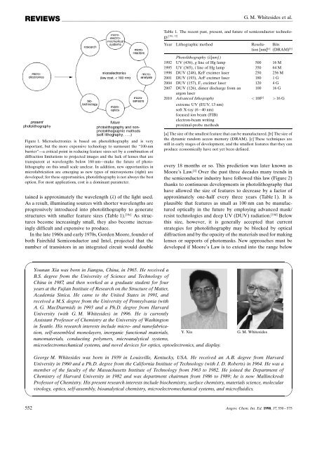
Figure 1. Microelectronics is based on photolithography and is very<br />
important, but the more expensive technology to surmount the ª100-nm<br />
barrierºÐa critical point in reducing feature sizes set by a combination of<br />
diffraction limitations to projected images and the lack of lenses that are<br />
transparent at wavelengths below 160 nmÐmake the future of photolithography<br />
on <strong>this</strong> small scale unclear. In addition, new opportunities in<br />
microfabrication are emerging as new types of microsystems (right) are<br />
developed; for these opportunities, photolithography is not always the best<br />
option. For most applications, cost is a dominant parameter.<br />
tained is approximately the wavelength (l) of the light used.<br />
As a result, illuminating sources <strong>with</strong> shorter wavelengths are<br />
progressively introduced into photolithography to generate<br />
structures <strong>with</strong> smaller feature sizes (Table 1). [10c] As structures<br />
become increasingly small, they also become increasingly<br />
difficult and expensive to produce.<br />
In the late 1960s and early 1970s, Gorden Moore, founder of<br />
both Fairchild Semiconductor and Intel, projected that the<br />
number of transistors in an integrated circuit would double<br />
[a] The size of the smallest feature that can be manufactured. [b] The size of<br />
the dynamic random access memory (DRAM). [c] These techniques are<br />
still in early stages of development, and the smallest features that they can<br />
produce economically have not yet been defined.<br />
every 18 months or so. This prediction was later known as<br />
Moores Law. [2] Over the past three decades many trends in<br />
the semiconductor industry have followed <strong>this</strong> law (Figure 2)<br />
thanks to continuous developments in photolithography that<br />
have allowed the size of features to decrease by a factor of<br />
approximately one-half every three years (Table 1). It is<br />
plausible that features as small as 100 nm can be manufactured<br />
optically in the future by employing advanced mask/<br />
resist technologies and deep UV (DUV) radiation. [10d] Below<br />
<strong>this</strong> size, however, it is generally accepted that current<br />
strategies for photolithography may be blocked by optical<br />
diffraction and by the opacity of the materials used for making<br />
lenses or supports of photomasks. New approaches must be<br />
developed if Moores Law is to extend into the range below<br />
Younan Xia was born in Jiangsu, China, in 1965. He received a<br />
B.S. degree from the University of Science and Technology of<br />
China in 1987, and then worked as a graduate student for four<br />
years at the Fujian Institute of Research on the Structure of Matter,<br />
Academia Sinica. He came to the United States in 1991, and<br />
received a M.S. degree from the University of Pennsylvania (<strong>with</strong><br />
A. G. MacDiarmid) in 1993 and a Ph.D. degree from Harvard<br />
University (<strong>with</strong> G. M. Whitesides) in 1996. He is currently<br />
Assistant Professor of Chemistry at the University of Washington<br />
in Seattle. His research interests include micro- and nanofabrication,<br />
self-assembled monolayers, inorganic functional materials,<br />
nanomaterials, conducting polymers, microanalytical systems,<br />
Y. Xia G. M. Whitesides<br />
microelectromechanical systems, and novel devices for optics, optoelectronics, and display.<br />
George M. Whitesides was born in 1939 in Louisville, Kentucky, USA. He received an A.B. degree from Harvard<br />
University in 1960 and a Ph.D. degree from the California Institute of Technology (<strong>with</strong> J. D. Roberts) in 1964. He was a<br />
member of the faculty of the Massachusetts Institute of Technology from 1963 to 1982. He joined the Department of<br />
Chemistry of Harvard University in 1982 and was department chairman from 1986 to 1989; he is now Mallinckrodt<br />
Professor of Chemistry. His present research interests include biochemistry, surface chemistry, materials science, molecular<br />
virology, optics, self-assembly, bioanalytical chemistry, microelectromechanical systems, and microfluidics.<br />
552 Angew. Chem. Int. Ed. 1998, 37, 550 ± 575