Replica molding with a polysiloxane mold provides this ... - EPFL
Replica molding with a polysiloxane mold provides this ... - EPFL
Replica molding with a polysiloxane mold provides this ... - EPFL

Create successful ePaper yourself
Turn your PDF publications into a flip-book with our unique Google optimized e-Paper software.
Soft Lithography<br />
REVIEWS<br />
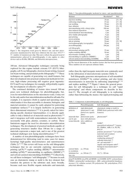
Table 2. Non-photolithographic methods for micro- and nanofabrication.<br />
Method Resolution [a] Ref.<br />
Figure 2. The integration trend given by Moores law, and how microprocessors<br />
manufactured by Intel have followed <strong>this</strong> law since 1973;<br />
[2b, c]<br />
N ˆ number of transistors per chip. This curve reflects the general trend of<br />
miniaturization achieved by microlithography; it also applies to other<br />
devices such as RAMs, DRAMs, and Motorola microprocessors.<br />
100 nm. Advanced lithographic techniques currently being<br />
explored for <strong>this</strong> regime include extreme UV (EUV) lithography,<br />
soft X-ray lithography, electron-beam writing, focused<br />
ion beam writing, and proximal-probe lithography. [11, 12] These<br />
techniques are capable of generating very small features, but<br />
their development into practical commercial methods for lowcost,<br />
high-volume processing still requires great ingenuity:<br />
EUVand X-ray techniques, for example, will probably require<br />
the development of reflective optics. [10d]<br />
The continued shrinking of feature sizes toward 100 nm<br />
poses new technical challenges for photolithography, but,<br />
even for microfabrication on the micrometer scale, it may not<br />
be the only and/or best microfabrication method for all tasks. For<br />
example, it is expensive (both in capital and operating cost),<br />
which makes it less than accessible to chemists, biologists, and<br />
material scientists; it cannot be easily adopted for patterning<br />
nonplanar surfaces; [13] it is largely ineffective in generating<br />
three-dimensional structures; [11a] it is poorly suited for introducing<br />
specific chemical functionalities; it is directly applicable<br />
to only a limited set of materials used as photoresists; [14]<br />
and it integrates well <strong>with</strong> semiconductor materials, but not<br />
necessarily <strong>with</strong> glass, plastics, ceramics, or carbon. These<br />
limitations suggest the need for alternative microfabrication<br />
techniques. The development of practical methods capable of<br />
generating structures smaller than 100 nm for a range of<br />
materials represents a major task, and is one of the greatest<br />
[11, 12]<br />
technical challenges now facing microfabrication.<br />
A number of non-photolithographic techniques have been<br />
demonstrated for fabricating (and in some cases for manufacturing)<br />
high-quality microstructures and nanostructures<br />
(Table 2). [15±38] This review will focus on the soft lithographic<br />
techniques that we are currently exploring: microcontact<br />
printing (mCP), [34] replica <strong><strong>mold</strong>ing</strong> (REM), [35] microtransfer<br />
<strong><strong>mold</strong>ing</strong> (mTM), [36] micro<strong><strong>mold</strong>ing</strong> in capillaries (MIMIC), [37]<br />
and solvent-assisted micro<strong><strong>mold</strong>ing</strong> (SAMIM). [38] Collectively,<br />
we call these techniques ªsoft lithographyº, [33] because in each<br />
case an elastomeric stamp or <strong>mold</strong> is the key element that<br />
transfers the pattern to the substrate and, more broadly,<br />
because each uses flexible organic molecules and materials<br />
injection <strong><strong>mold</strong>ing</strong> 10 nm [15, 16]<br />
embossing (imprinting) 25 nm [17, 18]<br />
cast <strong><strong>mold</strong>ing</strong> 50 nm [19, 20]<br />
laser ablation 70 nm [21, 22]<br />
micromachining <strong>with</strong> a sharp stylus 100 nm [23]<br />
laser-induced deposition 1 mm [24]<br />
electrochemical micromachining 1 mm [25]<br />
silver halide photography 5 mm [26]<br />
pad printing 20 mm [27]<br />
screen printing 20 mm [28]<br />
ink-jet printing 50 mm [29, 30]<br />
electrophotography (xerography) 50 mm [31]<br />
stereolithography 100 mm [32]<br />
soft lithography [33]<br />
microcontact printing (mCP) 35 nm [34, 84f]<br />
replica <strong><strong>mold</strong>ing</strong> (REM) 30 nm [35]<br />
microtransfer <strong><strong>mold</strong>ing</strong> (mTM) 1 mm [36]<br />
micro<strong><strong>mold</strong>ing</strong> in capillaries (MIMIC) 1 mm [37]<br />
solvent-assisted micro<strong><strong>mold</strong>ing</strong> (SAMIM) 60 nm [38]<br />
[a] The lateral dimension of the smallest feature that has been generated.<br />
These numbers do not represent ultimate limits.<br />
rather than the rigid inorganic materials now commonly used<br />
in the fabrication of microelectronic systems (Table 3).<br />
Soft lithography generates micropatterns of self-assembled<br />
monolayers (SAMs) [39] by contact printing, and also forms<br />
[17, 18]<br />
microstructures in materials by embossing (imprinting)<br />
and replica <strong><strong>mold</strong>ing</strong>. [19, 20] Figure 3 shows the general procedure<br />
for soft lithography in a technique we call ªrapid<br />
prototypingº and whose components we describe in Section<br />
2.5. The strength of soft lithography is in replicating<br />
rather than fabricating the master, but rapid prototyping and<br />
Table 3. Comparison of photolithography to soft lithography.<br />
Photolithography Soft lithography<br />
definition of<br />
patterns<br />
materials that<br />
can be patterned<br />
directly<br />
current limits<br />
to resolution<br />
minimum feature<br />
size<br />
rigid photomask<br />
(patterned Cr supported<br />
on a quartz<br />
plate)<br />
photoresists (polymers<br />
<strong>with</strong> photosensitive<br />
additives)<br />
elastomeric stamp or <strong>mold</strong> (a<br />
PDMS block patterned <strong>with</strong> relief<br />
features)<br />
photoresists [e]<br />
SAMs<br />
SAMs [a]<br />
unsensitized polymers [b±e] (epoxy,<br />
PU, PMMA, ABS, CA, PS, PE,<br />
PVC) [f]<br />
polymer precursors [c, d] (of carbon<br />
materials and ceramics)<br />
polymer beads [d]<br />
conducting polymers [d]<br />
[a, d]<br />
colloidal materials<br />
[c, d]<br />
sol ± gel materials<br />
organic and inorganic salts [d]<br />
biological macromolecules [d]<br />
ca. 250 nm see Table 2<br />
ca. 100 nm ()<br />
10 () ± 100 nm<br />
[a] mCP. [b] REM. [c] mTM. [d] MIMIC. [e] SAMIM. [f] PU: polyurethane;<br />
PMMA: poly(methyl methacrylate); ABS: poly(acrylonitrile-butadienestyrene);<br />
CA: cellulose acetate; PS: polystyrene; PE: polyethylene; PVC:<br />
poly(vinyl chloride).<br />
Angew. Chem. Int. Ed. 1998, 37, 550 ± 575 553