Charge Pump Clock Generation PLL for the Data Output Block of the ...
Charge Pump Clock Generation PLL for the Data Output Block of the ...
Charge Pump Clock Generation PLL for the Data Output Block of the ...
- No tags were found...

You also want an ePaper? Increase the reach of your titles
YUMPU automatically turns print PDFs into web optimized ePapers that Google loves.
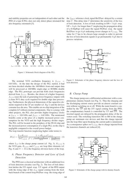
and stability properties are set independent <strong>of</strong> each o<strong>the</strong>r and <strong>the</strong><br />
PFD <strong>of</strong> a type II <strong>PLL</strong> does not only detect phase mismatch but<br />
also frequency mismatch [3].<br />
ffb<br />
f ref =40MHz<br />
Fb2Fast<br />
PFD<br />
Ref2Fast<br />
f out = 40 MHz<br />
UP<br />
DN<br />
CP<br />
LF<br />
3rd order<br />
V CTRL<br />
:2 :2 :2 :2<br />
80 MHz<br />
160 MHz<br />
320 MHz<br />
VCO<br />
640 MHz<br />
Figure 1: Schematic block diagram <strong>of</strong> <strong>the</strong> <strong>PLL</strong>.<br />
fVCO =16· fref<br />
<strong>the</strong> f REF reference clock signal Ref2Fast- delayed by a certain<br />
time T . This delay time T determines <strong>the</strong> sensitivity <strong>of</strong> <strong>the</strong> loss<br />
<strong>of</strong> lock detection. A loss <strong>of</strong> lock resulting in DN = high -resp.<br />
UP = high- <strong>for</strong> longer than T (neglecting <strong>the</strong> propagation delay<br />
<strong>of</strong> a D-flipflop) will cause <strong>the</strong> signal Fb2Fast -resp. <strong>the</strong> signal<br />
Ref2Fast- to go high indicating severe changes in V CTRL . The<br />
value <strong>for</strong> T has to be chosen large enough in order to prevent<br />
<strong>the</strong> loss <strong>of</strong> lock detection signals to go permanently high due to<br />
process variations.<br />
f REF<br />
f FB<br />
D<br />
D<br />
R<br />
R<br />
T<br />
Q<br />
Q<br />
T<br />
D<br />
&<br />
Q<br />
Ref2Fast<br />
UP<br />
DN<br />
D Q<br />
Fb2Fast<br />
The nominal VCO oscillation frequency is f VCO =<br />
640 MHz. At <strong>the</strong> time <strong>the</strong> design <strong>of</strong> <strong>the</strong> <strong>PLL</strong> started, it had<br />
not been decided whe<strong>the</strong>r <strong>the</strong> 160 Mbit/s front-end output data<br />
will be processed at 160 MHz single-edge or 80 MHz double<br />
edge. The <strong>PLL</strong> prototype can provide both clock frequencies<br />
derived from f VCO . Besides, <strong>the</strong> choice <strong>of</strong> a higher frequency<br />
f VCO eases <strong>the</strong> task <strong>of</strong> generating lower frequency outputs with<br />
a clean 50 % duty cycle required <strong>for</strong> double edge data processing.<br />
Fur<strong>the</strong>rmore, <strong>the</strong> physical dimensions <strong>of</strong> <strong>the</strong> capacitive elements<br />
required in <strong>the</strong> LF are smaller (cf. Eq. 1) and <strong>the</strong> devices<br />
consume less die area. This enables an on-chip integration <strong>of</strong> <strong>the</strong><br />
complete LF without external components. Due to synergy with<br />
o<strong>the</strong>r projects, <strong>the</strong> <strong>PLL</strong> also provides higher frequency clocks<br />
at f OUT = 320 MHz and f OUT = 640 MHz. The mentioned<br />
benefits come at <strong>the</strong> price <strong>of</strong> a slightly increased power consumption<br />
<strong>for</strong> <strong>the</strong> VCO and <strong>the</strong> high frequency divider stages.<br />
The <strong>PLL</strong> will be located in <strong>the</strong> periphery <strong>of</strong> <strong>the</strong> FE-I4 chip and<br />
<strong>the</strong> increased power consumption <strong>of</strong> a single <strong>PLL</strong> on <strong>the</strong> chip is<br />
negligible compared to <strong>the</strong> overall power budget.<br />
The loop transfer function (neglecting higher order terms) is<br />
H(s) = I CPK VCO<br />
2πC notch<br />
1+sR notch C notch<br />
s 2 + s I CP K VCO R notch<br />
2πN<br />
+ I CP K VCO<br />
(1)<br />
2πNC notch<br />
where I CP is <strong>the</strong> charge pump current (cf. Fig. 3), K VCO is<br />
<strong>the</strong> VCO gain, R notch and C notch are loop filter elements (cf.<br />
Fig. 4) and N =16is <strong>the</strong> frequency division factor <strong>of</strong> <strong>the</strong> loop.<br />
A. Phase Frequency Detector and Loss <strong>of</strong> Lock<br />
Detection<br />
The PFD uses a classical architecture with an additional loss<br />
<strong>of</strong> lock detection circuitry (see Fig. 2). The loss <strong>of</strong> lock detection<br />
latches <strong>the</strong> DN signal -resp. UP signal- <strong>of</strong> <strong>the</strong> PFD output<br />
with <strong>the</strong> rising edge <strong>of</strong> <strong>the</strong> f FB signal coming from <strong>the</strong> feedback<br />
branch <strong>of</strong> <strong>the</strong> control loop Fb2Fast -resp. <strong>the</strong> rising edge <strong>of</strong><br />
Figure 2: Schematic <strong>of</strong> <strong>the</strong> phase frequency detector and <strong>the</strong> loss <strong>of</strong><br />
lock detection.<br />
B. <strong>Charge</strong> <strong>Pump</strong><br />
The charge pump uses a differential architecture with a complementary<br />
dummy branch (see Fig. 3). Thus <strong>the</strong> charging and<br />
<strong>the</strong> discharging current source provide an almost constant current<br />
without switching on or <strong>of</strong>f. While <strong>the</strong> main branch is controlled<br />
by <strong>the</strong> UP and <strong>the</strong> DN signal coming from <strong>the</strong> PFD,<br />
<strong>the</strong> complementary branch is controlled by UP and DN. The<br />
inverted signals are delayed by <strong>the</strong> propagation delay <strong>of</strong> <strong>the</strong> inverters<br />
used. The switching transistors M1 to M4 in <strong>the</strong> charge<br />
pump are minimum size devices and thus <strong>the</strong> charge injected<br />
into <strong>the</strong> loop filter upon breaking <strong>the</strong> current path is minimized.<br />
As a consequence spikes on V CTRL due to charge injected from<br />
<strong>the</strong> transistor channels are reduced [4].<br />
UP<br />
R<br />
R<br />
DN<br />
1<br />
I CP<br />
M1<br />
M2<br />
I CP<br />
M3<br />
M4<br />
1<br />
CP OUT<br />
Figure 3: Schematic <strong>of</strong> <strong>the</strong> charge pump with its dummy branch.<br />
549