Charge Pump Clock Generation PLL for the Data Output Block of the ...
Charge Pump Clock Generation PLL for the Data Output Block of the ...
Charge Pump Clock Generation PLL for the Data Output Block of the ...
- No tags were found...

Create successful ePaper yourself
Turn your PDF publications into a flip-book with our unique Google optimized e-Paper software.
C. Loop Filter<br />
The first branch <strong>of</strong> <strong>the</strong> LF (cf. Fig. 4) with <strong>the</strong> capacitance<br />
C pole gives a low-pass characteristic to <strong>the</strong> control loop. However,<br />
<strong>the</strong> control loop is unstable with <strong>the</strong> associated frequency<br />
pole. The second branch <strong>of</strong> <strong>the</strong> LF (R notch , C notch ) creates<br />
a frequency notch in order to increase <strong>the</strong> phase margin <strong>of</strong> <strong>the</strong><br />
open-loop transfer function. By a rule <strong>of</strong> thumb 10 × C pole<br />
should be less than C notch in order to ensure sufficient phase<br />
margin. The third branch <strong>of</strong> <strong>the</strong> LF (R ripple ,C ripple ) <strong>for</strong>ms ano<strong>the</strong>r<br />
non-dominant frequency pole that filters high frequency<br />
noise on V CTRL . The characteristic frequency response <strong>of</strong><br />
<strong>the</strong> overall control loop can still be considered a second order<br />
system. The sum <strong>of</strong> all <strong>the</strong> capacitance values in <strong>the</strong> LF is<br />
C SUM ≈ 10 pF. All capacitors are vertical natural caps fully<br />
integrated on chip. The die area consumption <strong>of</strong> <strong>the</strong> <strong>PLL</strong> core is<br />
dominated by <strong>the</strong>se capacitor devices to a large extend.<br />
C pole<br />
R ripple<br />
R notch<br />
C notch<br />
C ripple<br />
Figure 4: Schematic <strong>of</strong> <strong>the</strong> loop filter.<br />
D. Differential Voltage-Controlled Oscillator<br />
The VCO consists <strong>of</strong> three inverters connected as a ring oscillator<br />
and a fourth inverter that serves as a buffer. The inverters<br />
are differential pairs loaded with PFET active loads and<br />
cross-coupled stages <strong>for</strong> rail-to-rail hard switching behavior (see<br />
Fig. 5).<br />
f VCO = 640 MHz is guaranteed <strong>for</strong> 3σ process variations without<br />
additional external tuning. The implemented VCO design is<br />
a trade-<strong>of</strong>f between an extended VCO tuning range and noise<br />
sensitivity.<br />
E. Frequency Dividers and <strong>Output</strong> Buffers<br />
The FDs consist <strong>of</strong> four custom-made divide by two toggleflipflops.<br />
The VCO output frequency <strong>of</strong> f VCO = 640 MHz is<br />
consecutively divided down to 320 MHz, 160 MHz, 80 MHz and<br />
finally to 40 MHz equaling a total frequency division factor <strong>of</strong><br />
N =16.<br />
In <strong>the</strong> output buffering stages, <strong>the</strong> differential clock signals from<br />
<strong>the</strong> dividing chain are converted to single-ended clock signals.<br />
Be<strong>for</strong>e <strong>the</strong> clock signals are sent out <strong>of</strong> <strong>the</strong> chip, <strong>the</strong> lower frequency<br />
clock signals are all gated with <strong>the</strong> 640 MHz clock <strong>for</strong><br />
clock alignment. It is also possible to disable <strong>the</strong> lower frequency<br />
clocks in order to save dynamic power consumption.<br />
The periphery <strong>of</strong> <strong>the</strong> test chip includes silicon proven LVDS<br />
drivers integrated into <strong>the</strong> pads that send <strong>the</strong> dynamic signals<br />
<strong>of</strong>f chip [1].<br />
III. INTEGRATED DIGITAL TEST LOGIC<br />
The digital test logic integrated on <strong>the</strong> fabricated <strong>PLL</strong> test<br />
chip consists <strong>of</strong> an eight bit pseudo random binary sequence<br />
generator, an eight bit ten bit coder and a serializer. The clock<br />
signal <strong>for</strong> <strong>the</strong> test logic can ei<strong>the</strong>r be an external clock or <strong>the</strong><br />
80 MHz single-ended output <strong>of</strong> <strong>the</strong> <strong>PLL</strong> core. The output data<br />
<strong>of</strong> <strong>the</strong> serializer is a 160 Mbit/s double data rate bit stream. The<br />
integration <strong>of</strong> <strong>the</strong> test logic on-chip provides a built-in self-test<br />
<strong>for</strong> <strong>the</strong> <strong>PLL</strong> output signal integrity. The test logic implemented<br />
resembles a large part <strong>of</strong> <strong>the</strong> future FE-I4 data output block.<br />
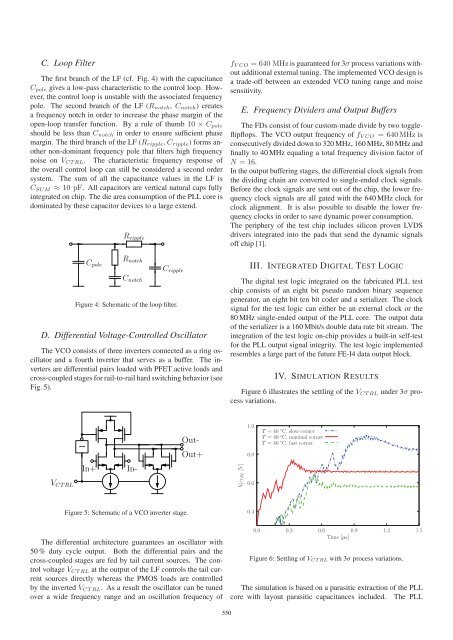
IV. SIMULATION RESULTS<br />
Figure 6 illustrates <strong>the</strong> settling <strong>of</strong> <strong>the</strong> V CTRL under 3σ process<br />
variations.<br />
1<br />
Out-<br />
Out+<br />
1.0<br />
0.8<br />
T =40 ◦ C, slow corner<br />
T =40 ◦ C, nominal corner<br />
T =40 ◦ C, fast corner<br />
V CTRL<br />
In+<br />
In-<br />
VCTRL [V]<br />
0.6<br />
Figure 5: Schematic <strong>of</strong> a VCO inverter stage.<br />
0.4<br />
The differential architecture guarantees an oscillator with<br />
50 % duty cycle output. Both <strong>the</strong> differential pairs and <strong>the</strong><br />
cross-coupled stages are fed by tail current sources. The control<br />
voltage V CTRL at <strong>the</strong> output <strong>of</strong> <strong>the</strong> LF controls <strong>the</strong> tail current<br />
sources directly whereas <strong>the</strong> PMOS loads are controlled<br />
by <strong>the</strong> inverted V CTRL . As a result <strong>the</strong> oscillator can be tuned<br />
over a wide frequency range and an oscillation frequency <strong>of</strong><br />
0.0 0.3 0.6 0.9 1.2 1.5<br />
Time [μs]<br />
Figure 6: Settling <strong>of</strong> V CTRL with 3σ process variations.<br />
The simulation is based on a parasitic extraction <strong>of</strong> <strong>the</strong> <strong>PLL</strong><br />
core with layout parasitic capacitances included. The <strong>PLL</strong><br />
550