Charge Pump Clock Generation PLL for the Data Output Block of the ...
Charge Pump Clock Generation PLL for the Data Output Block of the ...
Charge Pump Clock Generation PLL for the Data Output Block of the ...
- No tags were found...

You also want an ePaper? Increase the reach of your titles
YUMPU automatically turns print PDFs into web optimized ePapers that Google loves.
V CTRL settles in less than t settle =1.5 μs in all process corners.<br />
Under nominal conditions V CTRL settles in t settle ≈ 650 ns to<br />
an accuracy <strong>of</strong> 2 % <strong>of</strong> its final value. In order to investigate<br />
<strong>the</strong> <strong>PLL</strong> response to single-event transients, charges <strong>of</strong> 3 pC in<br />
1.5 ns pulses [5] have been injected into various nodes <strong>of</strong> <strong>the</strong><br />
control loop. Figure 7 shows <strong>the</strong> settling <strong>of</strong> V CTRL being interrupted<br />
by a charge injection at t = 900 ns into <strong>the</strong> very same<br />
node that controls <strong>the</strong> oscillation frequency <strong>of</strong> <strong>the</strong> VCO. Fur<strong>the</strong>rmore,<br />
Fig. 7 sketches <strong>the</strong> reaction <strong>of</strong> <strong>the</strong> loss <strong>of</strong> lock detection.<br />
While V CTRL is rising, <strong>the</strong> VCO is oscillating too<br />
slowly. Consequently <strong>the</strong> Ref2Fast signal is high, indicating<br />
that <strong>the</strong> reference clock is too fast resp. f VCO is too low. When<br />
<strong>the</strong> charge injection takes place V CTRL drastically increases,<br />
speeding-up <strong>the</strong> VCO and thus <strong>the</strong> Fb2Fast signal changes to<br />
high, indicating that <strong>the</strong> frequency <strong>of</strong> <strong>the</strong> signal coming from<br />
<strong>the</strong> feedback branch is higher than <strong>the</strong> input reference clock signal.<br />
<strong>Output</strong><br />
Connectors<br />
<strong>PLL</strong><br />
Chip<br />
LVDS<br />
Transceiver<br />
SMA<br />
Connector<br />
Power Connector Jumpers<br />
EN− Potentiometer<br />
Trim<br />
1.2<br />
1.0<br />
V CTRL<br />
Fb2Fast<br />
Ref2Fast<br />
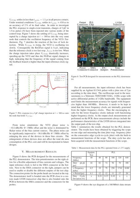
Figure 8: Test PCB designed <strong>for</strong> measurements on <strong>the</strong> <strong>PLL</strong> demonstrator.<br />
Voltage [V]<br />
0.8<br />
0.6<br />
0.4<br />
0.2<br />
0.0<br />
0.0 0.3 0.6 0.9 1.2 1.5<br />
Time [μs]<br />
Figure 7: <strong>PLL</strong> response to a 3 pC charge injection at t = 900 ns onto<br />
<strong>the</strong> node that holds V CTRL.<br />
From noise simulations <strong>the</strong> VCO phase noise is<br />
−83.3 dBc/Hz @ 1 MHz <strong>of</strong>fset and <strong>the</strong> noise is dominated by<br />
flicker noise <strong>of</strong> <strong>the</strong> bias current sources. The phase noise can<br />
be significantly improved to −90.0 dBc/Hz @ 1 MHz <strong>of</strong>fset by<br />
enlarging <strong>the</strong> area <strong>of</strong> <strong>the</strong> devices in <strong>the</strong>se bias circuits. The<br />
enlargement <strong>of</strong> <strong>the</strong>se devices does not affect <strong>the</strong> total die area<br />
consumption <strong>of</strong> <strong>the</strong> <strong>PLL</strong> core and will be incorporated in future<br />
designs.<br />
V. MEASUREMENT RESULTS<br />
Figure 8 shows <strong>the</strong> PCB designed <strong>for</strong> <strong>the</strong> measurements <strong>of</strong><br />
<strong>the</strong> <strong>PLL</strong> demonstrator. The trim potentiometers on <strong>the</strong> right allow<br />
<strong>for</strong> a flexible adjustment <strong>of</strong> bias currents and voltages. The<br />
input reference clock is fed to <strong>the</strong> SMA connector at <strong>the</strong> bottom.<br />
Next to <strong>the</strong> SMA connector on <strong>the</strong> right, jumpers can be<br />
used to enable or disable <strong>the</strong> different outputs <strong>of</strong> <strong>the</strong> test chip.<br />
The connection points <strong>for</strong> <strong>the</strong> probe heads are located at <strong>the</strong> top.<br />
The demonstrator itself is bonded onto <strong>the</strong> PCB close to a custom<br />
made LVDS transceiver chip that is also bonded onto <strong>the</strong><br />
PCB in between <strong>the</strong> SMA connector and <strong>the</strong> connectors <strong>for</strong> <strong>the</strong><br />
probes.<br />
For all measurements, <strong>the</strong> input reference clock has been<br />
supplied by an Agilent 81134A pulser with a jitter rms <strong>of</strong> 2 ps<br />
according to <strong>the</strong> data sheet. The oscilloscope used in <strong>the</strong> measurements<br />
is a Tektronix TDS5104B 5 GS/s, 1 GHz scope with<br />
active differential probes <strong>of</strong> 1 GHz bandwidth. The equipment<br />
used limits <strong>the</strong> measurement accuracy <strong>for</strong> signals with frequencies<br />
higher than 160 MHz. However, it needs to be kept in<br />
mind that <strong>the</strong> lower frequency clocks are internally generated<br />
from <strong>the</strong> higher frequency clocks. Thus <strong>the</strong> encouraging results<br />
<strong>for</strong> <strong>the</strong> lower frequency clocks indicate well functioning<br />
higher frequency clocks. As <strong>the</strong> output clock measurements are<br />
per<strong>for</strong>med on <strong>the</strong> PCB, <strong>the</strong>se measurements always include <strong>the</strong><br />
per<strong>for</strong>mance characteristics <strong>of</strong> <strong>the</strong> LVDS drivers integrated into<br />
<strong>the</strong> output pads <strong>of</strong> <strong>the</strong> test chip.<br />
Table 1 summarizes <strong>the</strong> results obtained <strong>for</strong> <strong>the</strong> <strong>PLL</strong> demonstrator.<br />
The results have been obtained by triggering <strong>the</strong> scope<br />
on one edge and measuring <strong>the</strong> time jitter resp. frequency jitter<br />
on <strong>the</strong> consecutive edge (cycle-to-cycle jitter) with <strong>the</strong> built-in<br />
measurement functions <strong>of</strong> <strong>the</strong> scope. The duty cycle has also<br />
been acquired with <strong>the</strong> measurement functions <strong>of</strong> <strong>the</strong> scope.<br />
Table 1: Measurement data <strong>for</strong> <strong>the</strong> <strong>PLL</strong> operated from a 1.2 V supply.<br />
Equipm.<br />
<strong>PLL</strong><br />
Test<br />
Frequency 40 40 80 160 320 640<br />
[MHz]<br />
Jitter pk-pk 44 82 74 94 70 106<br />
[ps]<br />
σ-Frequency 6.5 19 79 258 1710 8100<br />
[kHz]<br />
σ-Period [ps] 4.1 12 12 11 17 20<br />
Duty Cycle x 0.24 0.33 0.10 x x<br />
Deviation [%]<br />
Figure 9 shows <strong>the</strong> eye diagram <strong>of</strong> a 160 Mbit/s data stream<br />
551