XAPP112: Designing With XC9500XL CPLDs - App Note, V1.1 (01/99)
XAPP112: Designing With XC9500XL CPLDs - App Note, V1.1 (01/99)
XAPP112: Designing With XC9500XL CPLDs - App Note, V1.1 (01/99)

You also want an ePaper? Increase the reach of your titles
YUMPU automatically turns print PDFs into web optimized ePapers that Google loves.
R<br />
<strong>Designing</strong> <strong>With</strong> <strong>XC9500XL</strong> <strong>CPLDs</strong><br />
and reset product terms can assume the functionality of<br />
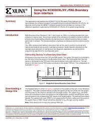
driving the flip flop clock enable. Figure 4 shows details of<br />
Product Term Allocation and Figure 5 and Figure 6 show<br />
how clock enable circuitry is created.<br />
Product Term<br />
Allocator<br />
Product Term<br />
Allocator<br />
Macrocell Logic<br />
<strong>With</strong> 2<br />
Product Terms<br />
In Figure 4, all but the Product Term Allocators have been<br />
omitted for clarity. In this situation, the design requirement<br />
is to deliver 18 product terms to the designated sum of<br />
product output site. The native set of 5 p-terms is supplemented<br />
with 5 p-terms from each directly adjacent neighbor<br />
taking the tally to 15 product terms. In this case, three more<br />
p-terms are needed, so the software must find them. The<br />
next site (to the north) requires two of its native 5 product<br />
terms, but three are available to meet the demand. The<br />
software forwards the available three p-terms to the<br />
required delivery site. In this case, two cascade times are<br />
required to provide 18 product terms. <strong>Note</strong> that the solution<br />
is not unique. The software could just as well encounter an<br />
adjacent neighbor with locked down product terms and<br />
been forced to skip over another macrocell to satisfy its<br />
need. The bidirectional cascade permits passing to/from<br />
both directions, which increases the likelihood of finding<br />
needed logic. This typically gives results within a single<br />
cascade and occasionally needs to go further. Product<br />
terms are located circularly so that the bottom macrocell<br />
can pass directly to the top macrocell and vice versa. An<br />
important factor here is that every macrocell has the same<br />
potential access to product terms.<br />
Product Term<br />
Allocator<br />
D/T<br />
EC<br />
><br />
S<br />
R<br />
Q<br />
To Out<br />
Figure 5: D/T Flip Flop Clock Enable Notation<br />
Product Term<br />
Allocator<br />
Figure 4: Product Term Allocation<br />
Macrocell Logic<br />
<strong>With</strong> 18<br />
Product Terms<br />
X5896<br />
D<br />
CE<br />
S<br />
D/T Q<br />
><br />
Figure 6: D/T Flip Flop Clock Enable Structure<br />
R<br />
To FastCONNECT<br />
To Out<br />
In Figure 5, the Flip Flop shows separate D/T and EC<br />
(clock enable) pins attached to the flop. Actually, the term<br />
clock enable is a misnomer, because as shown in Figure 6,<br />
it is simply a mux select pin that chooses between an external<br />
“D” pin and the flop's own Q output. Clock enable does<br />
introduce an additional control pin to be managed, but is<br />
often used in cases where designers would otherwise be<br />
tempted to gate the clock to obtain design control.<br />
Not emphasized in the macrocell diagram is the ability to<br />
selectively invert any clock entering the clock mux before<br />
attaching to the flip flop clock input point. Figure 7 details<br />
how this is achieved at every macrocell site.<br />
4 <strong>XAPP112</strong> January 22, 1<strong>99</strong>9 (Version 1.1)