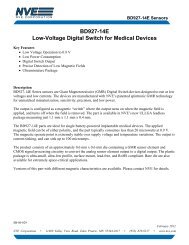
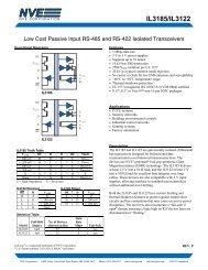
IL485 Product Data Sheet - NVE Corporation
IL485 Product Data Sheet - NVE Corporation
IL485 Product Data Sheet - NVE Corporation

You also want an ePaper? Increase the reach of your titles
YUMPU automatically turns print PDFs into web optimized ePapers that Google loves.
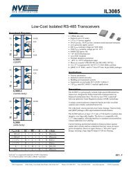
<strong>IL485</strong><br />
Isolated RS485 Interface<br />
Functional Diagram<br />
DE<br />
D<br />
R<br />
RE<br />
<strong>IL485</strong><br />
ISODE<br />
A<br />
B<br />
Features<br />
• 3.3 V Input Supply Compatible<br />
• 2500 V RMS Isolation (1 min.)<br />
• 25 ns Maximum Propagation Delay<br />
• 35 Mbps <strong>Data</strong> Rate<br />
• 1 ns Pulse Skew (typ.)<br />
• Designed for Multi-point Transmission<br />
on Long Bus Lines in Noisy Environments<br />
• ±60 mA Driver Output Capability<br />
• Thermal Shutdown Protection<br />
• Meets or Exceeds ANSI RS-485 and ISO 8482:1987(E)<br />
• −40°C to +85°C Temperature Range<br />
• PROFIBUS International Component Recognition<br />
• 16-Pin SOIC Package<br />
• UL1577 and IEC 61010-2001 Approval<br />
V ID (A−B) DE RE ISODE R D Mode<br />
≥ 200 mV L L L H X Receive<br />
≤−200 mV L L L L X Receive<br />
−7
<strong>IL485</strong><br />
Absolute Maximum Ratings (11)<br />
Parameters Symbol Min. Typ. Max. Units Test Conditions<br />
Storage Temperature T S −65 150 °C<br />
Ambient Operating Temperature T A −40 100 °C<br />
Voltage Range at A or B Bus Pins −7 12 V<br />
Supply Voltage (1) V DD1 , V DD2 −0.5 7 V<br />
Digital Input Voltage −0.5 V DD + 0.5 V<br />
Digital Output Voltage −0.5 V DD + 1 V<br />
Continuous Total Power Dissipation<br />
725<br />
25°C<br />
mW<br />
377<br />
85°C<br />
Maximum Output Current I O 95 mA<br />
Lead Solder Temperature 260 °C 10 sec.<br />
ESD 2 kV HBM<br />
Recommended Operating Conditions<br />
Parameters Symbol Min. Typ. Max. Units Test Conditions<br />
Supply Voltage<br />
V DD1<br />
3.0<br />
5.5<br />
V DD2<br />
4.5<br />
5.5<br />
V<br />
Input Voltage at any Bus Terminal<br />
(separately or common mode)<br />
12<br />
−7<br />
V<br />
V I<br />
V IC<br />
High-Level Digital Input Voltage<br />
V IH<br />
2.4<br />
3.0<br />
V DD1 V<br />
Low-Level Digital Input Voltage V IL 0 0.8 V<br />
Differential Input Voltage (2) V ID +12/−7 V<br />
High-Level Output Current (Driver) I OH 60 mA<br />
High-Level Digital Output Current<br />
(Receiver)<br />
I OH 8 mA<br />
Low-Level Output Current (Driver) I OL −60 mA<br />
Low-Level Digital Output Current<br />
(Receiver)<br />
I OL −8 mA<br />
Ambient Operating Temperature T A −40 85 °C<br />
Transient Immunity 20 kV/μs<br />
Digital Input Signal<br />
Rise and Fall Times<br />
t IR ,t IF<br />
DC Stable<br />
V DD1 = 3.3 V<br />
V DD1 = 5.0 V<br />
Insulation Specifications<br />
Parameters Symbol Min. Typ. Max. Units Test Conditions<br />
Creepage Distance 8.08 mm<br />
Barrier Impedance >10 14 ||7 Ω || pF<br />
Leakage Current 0.2 μA 240 V RMS , 60 Hz<br />
Safety and Approvals<br />
IEC61010-1<br />
TUV Certificate Numbers: N1502812, N1502812-101<br />
Classification: Reinforced Insulation<br />
Model Package Pollution Degree Material Group Max. Working Voltage<br />
<strong>IL485</strong> 0.3" SOIC II III 300 V RMS<br />
UL 1577<br />
Component Recognition Program File Number: E207481<br />
Rated 2500V RMS for 1 minute<br />
Soldering Profile<br />
Per JEDEC J-STD-020C, MSL=2<br />
2<br />
<strong>NVE</strong> <strong>Corporation</strong> 11409 Valley View Road Eden Prairie, MN 55344-3617 USA Telephone: (952) 829-9217 Fax (952) 829-9189 Internet: www.isoloop.com
<strong>IL485</strong><br />
<strong>IL485</strong> Pin Connections<br />
1 V DD1 Input Power Supply<br />
2 GND 1 Input Power Supply Ground Return<br />
3 R Output <strong>Data</strong> from Bus<br />
4 RE<br />
Read <strong>Data</strong> Enable<br />
(if RE is high, R = high impedance)<br />
5 DE Drive Enable<br />
6 D <strong>Data</strong> Input to Bus<br />
7 NC No Internal Connection<br />
8 GND 1 Input Power Supply Ground Return<br />
9 GND 2 Output Power Supply Ground Return<br />
10 ISODE<br />
Isolated DE Output for use in Profibus<br />
applications where the state of the isolated<br />
drive enable node needs to be monitored<br />
11 NC No Internal Connection<br />
12 A Non-inverting Bus Line<br />
13 B Inverting Bus Line<br />
14 NC No Internal Connection<br />
15 GND 2 Output Power Supply Ground Return.<br />
16 V DD2 Output Power Supply<br />
VDD 2<br />
VDD 1<br />
GND 1<br />
GND 2<br />
R<br />
NC<br />
RE<br />
B<br />
DE<br />
A<br />
D<br />
NC<br />
NC<br />
ISODE<br />
GND 2<br />
GND 1<br />
3<br />
<strong>NVE</strong> <strong>Corporation</strong> 11409 Valley View Road Eden Prairie, MN 55344-3617 USA Telephone: (952) 829-9217 Fax (952) 829-9189 Internet: www.isoloop.com
<strong>IL485</strong><br />
Driver Section<br />
Electrical Specifications are T min to T max and V DD = 4.5 V to 5.5 V, unless otherwise stated.<br />
Parameters Symbol Min. Typ. (5) Max. Units Test Conditions<br />
Input Clamp Voltage V IK −1.5 V I L = −18 mA<br />
Output voltage V O 0 6 V I O = 0<br />
Differential Output Voltage (2) |V OD1 | 1.5 6 V I O = 0<br />
Differential Output Voltage (2) |V OD2 | 1.5 2.5 5 V R L = 54 Ω, V DD = 5 V<br />
Differential Output Voltage (2)(6) V OD3 1.5 5 V R L = 54 Ω, V DD = 4.5 V<br />
Change in Magnitude of Differential<br />
Output Voltage (7) Δ|V OD | ±0.2 V R L = 54 Ω or 100 Ω<br />
3<br />
Common Mode Output Voltage V OC<br />
−1<br />
V R L = 54 Ω or 100 Ω<br />
Change in Magnitude of Common<br />
Mode Output Voltage (7) Δ|V OC | ±0.2 V R L = 54 Ω or 100 Ω<br />
Output Current (4) 1<br />
V<br />
Output Disabled<br />
I O<br />
mA<br />
O = 12 V<br />
−0.8<br />
V O = −7 V<br />
High Level Input Current I IH 10 μA V I = 3.5 V<br />
Low Level Input Current I IL −10 μA V I = 0.4 V<br />
Short-circuit Output Current I OS<br />
250<br />
−150 mA<br />
V O = −6 V<br />
V O = 0 V<br />
−250<br />
V O = 8 V<br />
Supply Current<br />
V DD1 = +5 V<br />
V DD1 = +3.3 V<br />
I DD1<br />
4<br />
I DD1 3<br />
6<br />
4<br />
mA<br />
No Load<br />
(Outputs Enabled)<br />
Switching Specifications<br />
Parameters Symbol Min. Typ. (5) Max. Units Test Conditions<br />
Maximum <strong>Data</strong> Rate 35 Mbps R L = 54 Ω, C L = 50 pF<br />
Differential Output Prop Delay t D (OD) 16 25 ns R L = 54 Ω, C L = 50 pF<br />
Pulse Skew (10) t S (P) 1 6 ns R L = 54 Ω, C L = 50 pF<br />
Differential Output Rise & Fall Time t T (OD) 8 10 ns R L = 54 Ω, C L = 50 pF<br />
Output Enable Time To High Level t PZH 31 65 ns R L = 54 Ω, C L = 50 pF<br />
Output Enable Time To Low Level t PZL 22 35 ns R L = 54 Ω, C L = 50 pF<br />
Output Disable Time From High Level t PHZ 28 50 ns R L = 54 Ω, C L = 50 pF<br />
Output Disable Time From Low Level t PLZ 16 32 ns R L = 54 Ω, C L = 50 pF<br />
Skew Limit (3) t SK (LIM) 2 12 ns R L = 54 Ω, C L = 50 pF<br />
Notes (apply to both driver and receiver sections):<br />
1. All voltage values are with respect to network ground except differential I/O bus voltages.<br />
2. Differential input/output voltage is measured at the noninverting terminal A with respect to the inverting terminal B.<br />
3. Skew limit is the maximum propagation delay difference between any two devices at 25°C.<br />
4. The power-off measurement in ANSI Standard EIA/TIA-422-B applies to disabled outputs only and<br />
is not applied to combined inputs and outputs.<br />
5. All typical values are at V DD1 ,V DD2 = 5 V or V DD1 = 3.3 V and T A = 25°C.<br />
6. The minimum V OD2 with a 100 Ω load is either ½ V OD1 or 2 V, whichever is greater.<br />
7. Δ|V OD | and Δ|V OC | are the changes in magnitude of V OD and V OC , respectively,<br />
that occur when the input is changed form one logic state to the other.<br />
8. This applies for both power on and power off, refer to ANSI standard RS-485 for exact condition.<br />
The EIA/TIA-422-B limit does not apply for a combined driver and receiver terminal.<br />
9. Includes 8 ns read enable time. Maximum propagation delay is 25 ns after read assertion.<br />
10. Pulse skew is defined as |t PLH − t PHL | of each channel.<br />
11. The relevant test and measurement methods are given in the Electromagnetic Compatibility section on p. 6.<br />
12. External magnetic field immunity is improved by this factor if the field direction is “end-to-end” rather than to “pin-to-pin” (see diagram on p. 6).<br />
4<br />
<strong>NVE</strong> <strong>Corporation</strong> 11409 Valley View Road Eden Prairie, MN 55344-3617 USA Telephone: (952) 829-9217 Fax (952) 829-9189 Internet: www.isoloop.com
<strong>IL485</strong><br />
Receiver Section<br />
Electrical Specifications are T min to T max and V DD = 4.5 V to 5.5 V, unless otherwise stated.<br />
Parameters Symbol Min. Typ. (5) Max. Units Test Conditions<br />
Positive-going Input<br />
V IT+ 0.2 V<br />
V O = 2.7 V,<br />
Threshold Voltage<br />
I O = −0.4 mA<br />
Negative-going Input<br />
V<br />
V<br />
Threshold Voltage<br />
IT- −0.2 V<br />
O = 0.5 V,<br />
I O = 8 mA<br />
Hysteresis Voltage (V IT+ − V IT- ) V HYS 60 mV<br />
High Level Digital Output Voltage V OH V DD − 0.2 V<br />
V ID = 200 mV<br />
I OH = −20 μA<br />
Low Level Digital Output Voltage V OL 0.2 V<br />
V ID = −200 mV<br />
I OH = 20 μA<br />
High-impedance-state output current I OZ ±20 μA V O = 0.4 to (V DD2 −0.5) V<br />
Line Input Current (8) I I −0.8 mA<br />
1<br />
Input Resistance r I 12 20 kΩ<br />
V I = 12 V<br />
V I = −7 V<br />
Other Input (11) = 0 V<br />
Supply Current I DD2 27 34 mA<br />
No load<br />
Outputs Enabled<br />
Switching Characteristics at 5 V<br />
Parameters Symbol Min. Typ. (5) Max. Units Test Conditions<br />
Maximum <strong>Data</strong> Rate 35 Mbps R L = 54 Ω, C L = 50 pF<br />
Propagation Delay (2, 9) t PD 24 32 ns<br />
V O = −1.5 V to 1.5 V,<br />
Pulse Skew (2, 10) t SK (P) 1 6 ns<br />
C L = 15 pF<br />
V O = −1.5 V to 1.5 V,<br />
C L = 15 pF<br />
Skew Limit (3) t SK (LIM) 2 8 ns R L = 54 Ω, C L = 50 pF<br />
Output Enable Time To High Level t PZH 17 24 ns C L = 15 pF<br />
Output Enable Time To Low Level t PZL 30 45 ns C L = 15 pF<br />
Output Disable Time From High Level t PHZ 30 45 ns C L = 15 pF<br />
Output Disable Time From Low Level t PLZ 18 27 ns C L = 15 pF<br />
Switching Characteristics at 3.3 V<br />
Parameters Symbol Min. Typ. (5) Max. Units Test Conditions<br />
Maximum <strong>Data</strong> Rate 35 Mbps R L = 54 Ω, C L = 50 pF<br />
Propagation Delay (2, 9) t PD 27 32 ns<br />
Pulse Skew (2, 10) t SK (P) 2 6 ns<br />
V O = −1.5 V to 1.5 V,<br />
C L = 15 pF<br />
V O = −1.5 V to 1.5 V,<br />
C L = 15 pF<br />
Skew Limit (3) t SK (LIM) 4 8 ns R L = 54 Ω, C L = 50 pF<br />
Output Enable Time to High Level t PZH 20 24 ns C L = 15 pF<br />
Output Enable Time to Low Level t PZL 33 45 ns C L = 15 pF<br />
Output Disable Time from High Level t PHZ 33 45 ns C L = 15 pF<br />
Output Disable Time from Low Level t PLZ 20 27 ns C L = 15 pF<br />
Magnetic Field Immunity (11)<br />
Magnetic Field Immunity at 5 V<br />
Power Frequency Magnetic Immunity H PF 2800 3500 A/m 50Hz/60Hz<br />
Pulse Magnetic Field Immunity H PM 4000 4500 A/m t p = 8µs<br />
Damped Oscillatory Magnetic Field H OSC 4000 4500 A/m 0.1Hz – 1MHz<br />
Cross-axis Immunity Multiplier (12) K X 2.5<br />
Magnetic Field Immunity at 3.3 V<br />
Power Frequency Magnetic Immunity H PF 1000 1500 A/m 50Hz/60Hz<br />
Pulse Magnetic Field Immunity H PM 1800 2000 A/m t p = 8µs<br />
Damped Oscillatory Magnetic Field H OSC 1800 2000 A/m 0.1Hz – 1MHz<br />
Cross-axis Immunity Multiplier (12) K X 2.5<br />
5<br />
<strong>NVE</strong> <strong>Corporation</strong> 11409 Valley View Road Eden Prairie, MN 55344-3617 USA Telephone: (952) 829-9217 Fax (952) 829-9189 Internet: www.isoloop.com
<strong>IL485</strong><br />
Application Information<br />
Electrostatic Discharge Sensitivity<br />
This product has been tested for electrostatic sensitivity to the<br />
limits stated in the specifications. However, <strong>NVE</strong> recommends that<br />
all integrated circuits be handled with appropriate care to avoid<br />
damage. Damage caused by inappropriate handling or storage could<br />
range from performance degradation to complete failure.<br />
Electromagnetic Compatibility<br />
The <strong>IL485</strong> is fully compliant with generic EMC standards<br />
EN50081, EN50082-1 and the umbrella line-voltage standard for<br />
Information Technology Equipment (ITE) EN61000. The<br />
IsoLoop Isolator’s Wheatstone bridge configuration and<br />
differential magnetic field signaling ensure excellent EMC<br />
performance against all relevant standards. <strong>NVE</strong> conducted<br />
compliance tests in the categories below:<br />
EN50081-1<br />
Residential, Commercial & Light Industrial<br />
Methods EN55022, EN55014<br />
EN50082-2: Industrial Environment<br />
Methods EN61000-4-2 (ESD), EN61000-4-3 (Electromagnetic<br />
Field Immunity), EN61000-4-4 (Electrical Transient Immunity),<br />
EN61000-4-6 (RFI Immunity), EN61000-4-8 (Power Frequency<br />
Magnetic Field Immunity), EN61000-4-9 (Pulsed Magnetic<br />
Field), EN61000-4-10 (Damped Oscillatory Magnetic Field)<br />
ENV50204<br />
Radiated Field from Digital Telephones (Immunity Test)<br />
Dynamic Power Consumption<br />
IsoLoop Isolators achieve their low power consumption from the<br />
way they transmit data across the isolation barrier. By detecting the<br />
edge transitions of the input logic signal and converting these to<br />
narrow current pulses, a magnetic field is created around the GMR<br />
Wheatstone bridge. Depending on the direction of the magnetic<br />
field, the bridge causes the output comparator to switch following<br />
the input logic signal. Since the current pulses are narrow, about<br />
2.5 ns, the power consumption is independent of mark-to-space<br />
ratio and solely dependent on frequency. This has obvious<br />
advantages over optocouplers, which have power consumption<br />
heavily dependent on frequency and time.<br />
The approximate power supply current per channel is:<br />
I IN = 40 x<br />
f<br />
x<br />
1<br />
mA<br />
f MAX 4<br />
Where f = operating frequency<br />
f MAX = 50 MHz<br />
Power Supply Decoupling<br />
Both V DD1 and V DD2 must be bypassed with 47 nF ceramic<br />
capacitors. These should be placed as close as possible to V DD pins<br />
for proper operation. Additionally, V DD2 should be bypassed with a<br />
10 µF tantalum capacitor.<br />
Immunity to external magnetic fields is even higher if the field<br />
direction is “end-to-end” rather than to “pin-to-pin” as shown in the<br />
diagram below:<br />
Cross-axis Field Direction<br />
6<br />
<strong>NVE</strong> <strong>Corporation</strong> 11409 Valley View Road Eden Prairie, MN 55344-3617 USA Telephone: (952) 829-9217 Fax (952) 829-9189 Internet: www.isoloop.com
<strong>IL485</strong><br />
0.3" 16-pin SOIC Package<br />
Dimensions in inches (mm)<br />
0.013 (0.3)<br />
0.020 (0.5)<br />
0.287 (7.29)<br />
0.300 (7.62)<br />
NOM<br />
0.397 (10.1)<br />
0.413 (10.5)<br />
0.007 (0.2)<br />
0.013 (0.3)<br />
0.016 (0.4)<br />
0.050 (1.3)<br />
Pin 1 identified by<br />
either an indent<br />
or a marked dot<br />
<br />
0.08 (2.0)<br />
0.10 (2.5)<br />
0.092 (2.34)<br />
0.105 (2.67)<br />
0.394 (10.00)<br />
0.419 (10.64)<br />
0.040 (1.0)<br />
NOTE: Pin spacing is a BASIC0.060 (1.5)<br />
dimension; tolerances <br />
do not accumulate<br />
0.004 (0.1)<br />
0.012 (0.3)<br />
Ordering Information and Valid Part Numbers<br />
IL 485 E TR13<br />
Bulk Packaging<br />
Blank = Tube<br />
TR = 13'' Tape and Reel<br />
Package<br />
Blank = 80/20 Tin/Lead Plating<br />
E = RoHS Compliant<br />
Base Part Number<br />
485 = RS-485 Transceiver<br />
Valid Part Numbers<br />
<strong>IL485</strong><br />
<strong>IL485</strong>E<br />
All <strong>IL485</strong><br />
part types are<br />
available on<br />
tape and reel.<br />
<strong>Product</strong> Family<br />
IL = Isolators<br />
RoHS<br />
COMPLIANT<br />
7<br />
<strong>NVE</strong> <strong>Corporation</strong> 11409 Valley View Road Eden Prairie, MN 55344-3617 USA Telephone: (952) 829-9217 Fax (952) 829-9189 Internet: www.isoloop.com
<strong>IL485</strong><br />
ISB-DS-001-<strong>IL485</strong>-Q<br />
March 2008<br />
Changes<br />
• Added magnetic field immunity and electromagnetic compatibility specifications.<br />
• Added note on package drawing that pin-spacing tolerances are non-accumulating.<br />
ISB-DS-001-<strong>IL485</strong>-P<br />
ISB-DS-001-<strong>IL485</strong>-O<br />
ISB-DS-001-<strong>IL485</strong>-N<br />
ISB-DS-001-<strong>IL485</strong>-M<br />
ISB-DS-001-<strong>IL485</strong>-L<br />
ISB-DS-001-<strong>IL485</strong>-K<br />
ISB-DS-001-<strong>IL485</strong>-J<br />
Changes<br />
• Changed ordering information to reflect that devices are now fully RoHS compliant<br />
with no exemptions.<br />
Changes<br />
• Reorganized supply current specifications; misc. minor changes<br />
Changes<br />
• Eliminated soldering profile chart<br />
Changes<br />
• Updated open input state in truth table<br />
Changes<br />
• Updated package drawing; misc. changes<br />
Changes<br />
• Update UL and IEC approvals<br />
Changes<br />
• Revision letter added.<br />
• Ordering Information Removed.<br />
• IEC 61010-1 “Reinforced Insulation” added.<br />
• Notes added.<br />
• PagIR Soldering Profile added<br />
• Ordering Information added.<br />
8<br />
<strong>NVE</strong> <strong>Corporation</strong> 11409 Valley View Road Eden Prairie, MN 55344-3617 USA Telephone: (952) 829-9217 Fax (952) 829-9189 Internet: www.isoloop.com
<strong>IL485</strong><br />
About <strong>NVE</strong><br />
An ISO 9001 Certified Company<br />
<strong>NVE</strong> <strong>Corporation</strong> manufactures innovative products based on unique spintronic Giant Magnetoresistive (GMR) technology. <strong>Product</strong>s include<br />
Magnetic Field Sensors, Magnetic Field Gradient Sensors (Gradiometers), Digital Magnetic Field Sensors, Digital Signal Isolators, and Isolated<br />
Bus Transceivers.<br />
<strong>NVE</strong> pioneered spintronics and in 1994 introduced the world’s first products using GMR material, a line of ultra-precise magnetic sensors for<br />
position, magnetic media, gear speed and current sensing.<br />
<strong>NVE</strong> <strong>Corporation</strong><br />
11409 Valley View Road<br />
Eden Prairie, MN 55344-3617 USA<br />
Telephone: (952) 829-9217<br />
Fax: (952) 829-9189<br />
Internet: www.nve.com<br />
e-mail: isoinfo@nve.com<br />
The information provided by <strong>NVE</strong> <strong>Corporation</strong> is believed to be accurate. However, no responsibility is assumed by <strong>NVE</strong> <strong>Corporation</strong> for its use,<br />
nor for any infringement of patents, nor rights or licenses granted to third parties, which may result from its use. No license is granted by<br />
implication, or otherwise, under any patent or patent rights of <strong>NVE</strong> <strong>Corporation</strong>. <strong>NVE</strong> <strong>Corporation</strong> does not authorize, nor warrant, any <strong>NVE</strong><br />
<strong>Corporation</strong> product for use in life support devices or systems or other critical applications, without the express written approval of the<br />
President of <strong>NVE</strong> <strong>Corporation</strong>.<br />
Specifications shown are subject to change without notice.<br />
ISB-DS-001-<strong>IL485</strong>-Q<br />
March 2008<br />
9<br />
<strong>NVE</strong> <strong>Corporation</strong> 11409 Valley View Road Eden Prairie, MN 55344-3617 USA Telephone: (952) 829-9217 Fax (952) 829-9189 Internet: www.isoloop.com