IL41050 Isolated CAN Transceiver Datasheet - NVE Corporation
IL41050 Isolated CAN Transceiver Datasheet - NVE Corporation
IL41050 Isolated CAN Transceiver Datasheet - NVE Corporation

Create successful ePaper yourself
Turn your PDF publications into a flip-book with our unique Google optimized e-Paper software.
<strong>IL41050</strong><br />
<strong>Isolated</strong> High-Speed <strong>CAN</strong> <strong>Transceiver</strong><br />
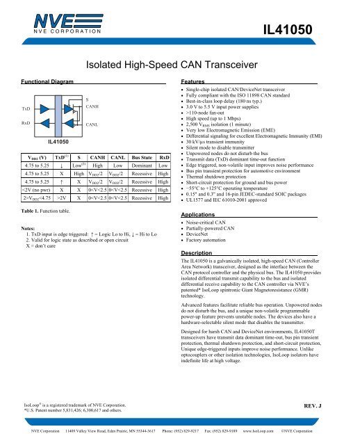
Functional Diagram<br />
TxD<br />
RxD<br />
<strong>IL41050</strong><br />
S<br />
<strong>CAN</strong>H<br />
<strong>CAN</strong>L<br />
V DD2 (V) TxD (1) S <strong>CAN</strong>H <strong>CAN</strong>L Bus State RxD<br />
4.75 to 5.25 ↓ Low (2) High Low Dominant Low<br />
4.75 to 5.25 X High V DD2 /2 V DD2 /2 Recessive High<br />
4.75 to 5.25 ↑ X V DD2 /2 V DD2 /2 Recessive High<br />
<strong>IL41050</strong><br />
(1) (2)<br />
Absolute Maximum Ratings<br />
Parameters Symbol Min. Typ. Max. Units Test Conditions<br />
Storage temperature T S −55 150 °C<br />
Ambient operating temperature T A −55 135 °C<br />
DC voltage at <strong>CAN</strong>H and <strong>CAN</strong>L pins V <strong>CAN</strong>H V <strong>CAN</strong>L −27 40 V<br />
0 V< V DD2 < 5.25 V;<br />
indefinite duration<br />
Supply voltage V DD1 , V DD2 −0.5 6 V<br />
Digital input voltage V TxD , V S −0.3 V DD + 0.3 V<br />
Digital output voltage V RxD −0.3 V DD + 0.3 V<br />
DC voltage at V REF V REF −0.3 V DD + 0.3 V<br />
Transient Voltage at <strong>CAN</strong>H or <strong>CAN</strong>L V trt(<strong>CAN</strong>) −200 200 V<br />
Electrostatic discharge at all pins V esd −4,000 4,000 V Human body model<br />
Electrostatic discharge at all pins V esd −200 200 V Machine model<br />
Recommended Operating Conditions<br />
Parameters Symbol Min. Typ. Max. Units Test Conditions<br />
V<br />
Supply voltage<br />
DD1<br />
3.0<br />
5.5<br />
V<br />
V DD2<br />
4.75<br />
5.25<br />
Input voltage at any bus terminal<br />
V <strong>CAN</strong>H<br />
−12 12 V<br />
(separately or common mode)<br />
V <strong>CAN</strong>L<br />
(3) (4)<br />
High-level digital input voltage V<br />
IH<br />
2.0<br />
2.4<br />
2.0<br />
V DD1<br />
V DD1<br />
V DD2<br />
V<br />
V DD1 = 3.3 V<br />
V DD1 = 5.0 V<br />
V DD2 = 5.0 V<br />
Low-level digital input voltage (3) (4) V IL 0 0.8 V<br />
Digital output current (RxD) I OH −8 8 mA V DD1 = 3.3V to 5V<br />
Ambient operating temperature T A −55 125 °C<br />
Digital input signal rise and fall times t IR , t IF 1 μs<br />
Insulation Specifications<br />
Parameters Symbol Min. Typ. Max. Units Test Conditions<br />
Creepage distance (external) 8.08 mm<br />
Barrier impedance > 10 14 || 7 Ω || pF<br />
Leakage current 0.2 μA RMS 240 V RMS , 60 Hz<br />
Safety and Approvals<br />
IEC61010-2001<br />
TUV Certificate Numbers:<br />
N1502812 (pending)<br />
Classification: Reinforced Insulation<br />
Model Package Pollution Degree Material Group Max. Working Voltage<br />
<strong>IL41050</strong> SOIC (0.15" and 0.3") II III 300 V RMS<br />
UL 1577<br />
Component Recognition Program File Number: E207481<br />
Rated 2,500V RMS for 1 minute<br />
Soldering Profile<br />
Per JEDEC J-STD-020C<br />
Moisture Sensitivity Level: MSL=2<br />
Notes:<br />
1. Absolute Maximum specifications mean the device will not be damaged if operated under these conditions. It does not guarantee performance.<br />
2. All voltages are with respect to network ground except differential I/O bus voltages.<br />
3. The TxD input is edge sensitive. Voltage magnitude of the input signal is specified, but edge rate specifications must also be met.<br />
4. The maximum time allowed for a logic transition at the TxD input is 1 μs.<br />
2<br />
<strong>NVE</strong> <strong>Corporation</strong> 11409 Valley View Road, Eden Prairie, MN 55344-3617 Phone: (952) 829-9217 Fax: (952) 829-9189 www.IsoLoop.com ©<strong>NVE</strong> <strong>Corporation</strong>
<strong>IL41050</strong><br />
<strong>IL41050</strong>-3 Pin Connections (0.15" SOIC Package)<br />
1 V DD1 V DD1 power supply input<br />
2 GND 1 V DD1 power supply ground return<br />
3 T D Transmit Data input<br />
4 RxD Receive Data output<br />
5 NC No internal connection<br />
6 NC No internal connection<br />
7 NC No internal connection<br />
8 NC No internal connection<br />
9 IsoRxD<br />
<strong>Isolated</strong> RxD output.<br />
No connection should be made to this pin.<br />
10 <strong>CAN</strong>L Low level <strong>CAN</strong>bus line<br />
11 V DD2 V DD2 <strong>CAN</strong> I/O bus circuitry power supply input*<br />
12 <strong>CAN</strong>H High level <strong>CAN</strong>bus line<br />
13 S<br />
Mode select input. Leave open or set low for<br />
normal operation; set high for silent mode.<br />
14 IsoTxD<br />
<strong>Isolated</strong> TxD output.<br />
No connection should be made to this pin.<br />
15 GND 2 V DD2 power supply ground return<br />
16 V DD2 V DD2 isolation power supply input*<br />
V DD1<br />
GND 1<br />
TxD<br />
RxD<br />
NC<br />
NC<br />
NC<br />
NC<br />
V DD2<br />
GND 2<br />
IsoTxD<br />
S<br />
<strong>CAN</strong>H<br />
V DD2<br />
<strong>CAN</strong>L<br />
IsoRxD<br />
<strong>IL41050</strong> Pin Connections (0.3" SOIC Package)<br />
1 V DD1 V DD1 power supply input<br />
V<br />
2 GND DD1 power supply ground return<br />
1<br />
(pin 2 is internally connected to pin 8)<br />
3 TxD Transmit Data input<br />
4 NC No internal connection<br />
5 RxD Receive Data output<br />
6 NC No internal connection<br />
7 NC No internal connection<br />
V<br />
8 GND DD1 power supply ground return<br />
1<br />
(pin 8 is internally connected to pin 2)<br />
V<br />
9 GND DD2 power supply ground return<br />
2<br />
(pin 9 is internally connected to pin 15)<br />
10 V REF<br />
Reference voltage output<br />
(nominally 50% of V DD2 )<br />
11 V DD2 V DD2 <strong>CAN</strong> I/O bus circuitry power supply input*<br />
12 <strong>CAN</strong>L Low level <strong>CAN</strong>bus line<br />
13 <strong>CAN</strong>H High level <strong>CAN</strong>bus line<br />
14 S<br />
Mode select input. Leave open or set low for<br />
normal operation; set high for silent mode.<br />
V<br />
15 GND DD2 power supply ground return<br />
2<br />
(pin 15 is internally connected to pin 9)<br />
16 V DD2 V DD2 isolation power supply input*<br />
V DD2<br />
GND 2<br />
GND 1<br />
GND 2<br />
TxD<br />
S<br />
NC<br />
<strong>CAN</strong>H<br />
RxD<br />
<strong>CAN</strong>L<br />
NC<br />
V DD2<br />
NC<br />
V REF<br />
GND 1<br />
V DD1<br />
*NOTE: Pin 11 is not internally connected to pin 16; both should be connected to the V DD2 power supply for normal operation.<br />
3<br />
<strong>NVE</strong> <strong>Corporation</strong> 11409 Valley View Road, Eden Prairie, MN 55344-3617 Phone: (952) 829-9217 Fax: (952) 829-9189 www.IsoLoop.com ©<strong>NVE</strong> <strong>Corporation</strong>
<strong>IL41050</strong><br />
Specifications<br />
Electrical Specifications are T min to T max and V DD1 , V DD2 = 4.75 V to 5.25 V unless otherwise stated.<br />
Parameters Symbol Min. Typ. Max. Units Test Conditions<br />
Power Supply Current<br />
Quiescent supply current (recessive)<br />
Dynamic supply current (dominant)<br />
IQ VDD1<br />
I VDD1<br />
1<br />
0.7<br />
1.2<br />
0.9<br />
4<br />
1.75<br />
1.4<br />
2.0<br />
1.6<br />
3.0<br />
2.0<br />
3.2<br />
2.2<br />
mA<br />
mA<br />
dr = 0 bps; V DD1 = 5 V<br />
dr = 0 bps; V DD1 = 3.3 V<br />
dr = 1 Mbps, R L = 60Ω;<br />
V DD1 = 5 V<br />
dr = 1 Mbps, R L = 60Ω;<br />
V DD1 = 3.3 V<br />
Quiescent supply current (recessive) IQ VDD2 3.5 6.75 13<br />
0 bps<br />
mA<br />
Dynamic supply current (dominant) I VDD2<br />
26 52 78<br />
1 Mbps, R L = 60Ω<br />
Transmitter Data input (TxD) (1)<br />
High level input voltage ↑ V IH 2.4 5.25 V V DD1 = 5 V; recessive<br />
High level input voltage ↑ V IH 2.0 3.6 V V DD1 = 3.3 V; recessive<br />
Low level input voltage ↓ V IL −0.3 0.8 V Output dominant<br />
TxD input rise and fall time (2) tr 1 μs 10% to 90%<br />
High level input current I IH −10 10 μA V TxD = V DD1<br />
Low level input current I IL 10 10 μA V TxD = 0 V<br />
Mode select input (S)<br />
High level input voltage V IH 2.0 V DD2 + 0.3 V Silent mode<br />
Low level input voltage V IL −0.3 0.8 V High-speed mode<br />
High level input current I IH 20 30 45 μA V S = 2 V<br />
Low level input current I IL 15 30 10 μA V S = 0 V<br />
Receiver Data output (RxD)<br />
High level output current I OH −2 −8.5 −20 mA V RxD = 0.8 V DD1<br />
Low level output current I OL 2 8.5 20 mA V RxD = 0.45 V<br />
Failsafe supply voltage (4) V DD2 3.6 3.9 V<br />
Reference Voltage output (V REF )<br />
Reference Voltage output V REF 0.45 V DD2 0.5 V DD2 0.55 V DD2 V −50 μA
<strong>IL41050</strong><br />
Specifications (...cont.)<br />
Electrical Specifications are T min to T max and V DD1 , V DD2 = 4.5 V to 5.5 V unless otherwise stated.<br />
Differential input capacitance C i(dif) 3.75 10 pF V TxD = V DD1<br />
Input leakage current at <strong>CAN</strong>H I LI(<strong>CAN</strong>H) 100 170 250 μA V <strong>CAN</strong>H = 5 V, V DD2 = 0 V<br />
Input leakage current at <strong>CAN</strong>L I LI(<strong>CAN</strong>L) 100 170 250 μA V <strong>CAN</strong>L = 5 V, V DD2 = 0 V<br />
Thermal Shutdown<br />
Shutdown junction temperature T j(SD) 155 165 180 °C<br />
Timing Characteristics<br />
TxD to bus active delay<br />
t d(TxD-BUSon)<br />
29 63 125<br />
V<br />
ns<br />
S = 0 V; V DD1 = 5 V<br />
32 66 128<br />
V S = 0 V; V DD1 = 3.3 V<br />
TxD to bus inactive delay<br />
t d(TxD-BUSoff)<br />
29 68 110<br />
V<br />
ns<br />
S = 0 V; V DD1 = 5 V<br />
32 71 113<br />
V S = 0 V; V DD1 = 3.3 V<br />
Bus active to RxD delay<br />
t d(BUSon-RxD)<br />
24 58 125<br />
V<br />
ns<br />
S = 0 V; V DD1 = 5 V<br />
27 61 128<br />
V S = 0 V; V DD1 = 3.3 V<br />
49 103 170<br />
V<br />
Bus inactive to RxD delay<br />
t d(BUSoff-RxD)<br />
ns<br />
S = 0 V; V DD1 = 5 V<br />
52 106 173<br />
V S = 0 V; V DD1 = 3.3 V<br />
Loop delay low-to-high or high-to-low T LOOP 53 180 210 ns V S = 0 V<br />
TxD dominant time for timeout T dom(TxD) 250 457 765 μs<br />
V TxD = 0 V<br />
3.0 V > V DD1 < 5.5 V<br />
Magnetic Field Immunity (3)<br />
V DD1 = 5 V, V DD2 = 5 V<br />
Power frequency magnetic immunity H PF 2,500 3,000 A/m 50 Hz/60 Hz<br />
Pulse magnetic field immunity H PM 3,000 3,500 A/m t p = 8 µs<br />
Cross-axis immunity multiplier K X 1.8 Figure 1<br />
V DD1 = 3.3 V, V DD2 = 5 V<br />
Power frequency magnetic immunity H PF 1,000 1,500 A/m 50 Hz/60 Hz<br />
Pulse magnetic field immunity H PM 1,800 2,000 A/m t p = 8 µs<br />
Cross-axis immunity multiplier K X 1.5 Figure 1<br />
Notes:<br />
1. The TxD input is edge sensitive. Voltage magnitude of the input signal is specified, but edge rate specifications must also be met.<br />
2. The maximum time allowed for a logic transition at the TxD input is 1 μs.<br />
3. Uniform magnetic field applied across the pins of the device. Cross-axis multiplier effective when field is applied perpendicular to the pins.<br />
4. If V DD2 falls below the specified failsafe supply voltage, RxD will go High.<br />
Electrostatic Discharge Sensitivity<br />
This product has been tested for electrostatic sensitivity to the limits stated in the specifications. However, <strong>NVE</strong> recommends that all integrated<br />
circuits be handled with appropriate care to avoid damage. Damage caused by inappropriate handling or storage could range from performance<br />
degradation to complete failure.<br />
Electromagnetic Compatibility<br />
The <strong>IL41050</strong> is fully compliant with generic EMC standards EN50081, EN50082-1 and the umbrella line-voltage standard for Information<br />
Technology Equipment (ITE) EN61000. The IsoLoop Isolator’s Wheatstone bridge configuration and differential magnetic field signaling ensure<br />
excellent EMC performance against all relevant standards. <strong>NVE</strong> conducted compliance tests in the categories below:<br />
EN50081-1<br />
Residential, Commercial & Light Industrial<br />
Methods EN55022, EN55014<br />
EN50082-2: Industrial Environment<br />
Methods EN61000-4-2 (ESD), EN61000-4-3 (Electromagnetic Field Immunity), EN61000-4-4 (Electrical Transient Immunity),<br />
EN61000-4-6 (RFI Immunity), EN61000-4-8 (Power Frequency Magnetic Field Immunity), EN61000-4-9 (Pulsed Magnetic<br />
Field), EN61000-4-10 (Damped Oscillatory Magnetic Field)<br />
ENV50204<br />
Radiated Field from Digital Telephones (Immunity Test)<br />
Immunity to external magnetic fields is higher if the field direction is “end-to-end” (rather than to “pin-to-pin”) as shown in the<br />
diagram at right. Fig. 1<br />
5<br />
<strong>NVE</strong> <strong>Corporation</strong> 11409 Valley View Road, Eden Prairie, MN 55344-3617 Phone: (952) 829-9217 Fax: (952) 829-9189 www.IsoLoop.com ©<strong>NVE</strong> <strong>Corporation</strong>
<strong>IL41050</strong><br />
Application Information<br />
V DD2<br />
Power Supply Pins<br />
Both V DD2 power supply inputs (pins 11 and 16) must be connected to the bus-side power supply. Pin 11 powers the bus side of the <strong>CAN</strong> I/O<br />
circuitry, while pin 16 powers the bus-side isolation circuitry. For testing purposes, they are not internally connected, but the part will not operate<br />
without both pins powered, and operation without both pins powered can cause damage.<br />
Power Supply Decoupling<br />
Both V DD1 and V DD2 must be bypassed with 100 nF ceramic capacitors. These supply the dynamic current required for the isolator switching and<br />
should be placed as close as possible to V DD and their respective ground return pins.<br />
Input Configurations<br />
The TxD input should not be left open as the state will be indeterminate. If connected to an open-drain or open collector output, a pull-up resistor<br />
(typically 16 kΩ) should be connected from the input to V DD1 .<br />
The Mode Select (“S”) input has a nominal 150 kΩ internal pull-down resistor. It can be left open or set low for normal operation.<br />
Dominant Mode Time-out and Failsafe Receiver Functions<br />
<strong>CAN</strong> bus latch up is prevented by an integrated Dominant mode timeout function. If the TxD pin is forced permanently low by hardware or<br />
software application failure, the time-out returns the RxD output to the high state no more than 765 μs after TxD is asserted dominant. The timer<br />
is triggered by a negative edge on TxD. If the duration of the low is longer than the internal timer value, the transmitter is disabled, driving the<br />
bus to the recessive state. The timer is reset by a positive edge on pin TxD.<br />
If power is lost on Vdd2, the <strong>IL41050</strong> asserts the RxD output high when the supply voltage falls below 3.8 V. RxD will return to normal<br />
operation as soon as Vdd2 rises above approximately 4.2 V.<br />
Programmable Power-Up<br />
A unique non-volatile programmable power-up feature prevents unstable nodes. A state that needs to be present at node power up can be<br />
programmed at the last power down. For example if a <strong>CAN</strong> node is required to “pulse” dominant at power up, TxD can be sent low by the<br />
controller immediately prior to power down. When power is resumed, the node will immediately go dominant allowing self-check code in the<br />
microcontroller to verify node operation. If desired, the node can also power up silently by presetting the TxD line high at power down. At the<br />
next power on, the <strong>IL41050</strong> will remain silent, awaiting a dominant state from the bus.<br />
The microcontroller can check that the <strong>CAN</strong> node powered down correctly before applying power at the next “power on” request. If the node<br />
powered down as intended, RxD will be set high and stored in <strong>IL41050</strong>’s non-volatile memory. The level stored in the RxD bit can be read<br />
before isolated node power is enabled, avoiding possible <strong>CAN</strong> bus disruption due to an unstable node.<br />
Replacing Non-<strong>Isolated</strong> <strong>Transceiver</strong>s<br />
The <strong>IL41050</strong> is designed to replace common non-isolated <strong>CAN</strong> transceivers such as the Philips/NXP TJA1050 with minimal circuit changes.<br />
Some notable differences:<br />
• Some non-isolated <strong>CAN</strong> transceivers have internal TxD pull-up resistors, but the <strong>IL41050</strong> TxD input should not be left open. If<br />
connected to an open-drain or open collector output, a pull-up resistor (typically 16 kΩ) should be connected from the input to V DD1 .<br />
• Initialization behavior varies between <strong>CAN</strong> transceivers. To ensure the desired power-up state, the <strong>IL41050</strong> should be initialized with a<br />
TxD pulse (low-to-high for recessive initialization), or shut down the transceiver in the desired power-up state (the “programmable<br />
power-up feature”).<br />
• Many non-isolated <strong>CAN</strong> transceivers have a V REF output. Such a reference is available on the <strong>IL41050</strong> wide-body version.<br />
The VREF Output<br />
V REF is a reference voltage output used to drive bus threshold comparators in some legacy systems and is provided on the <strong>IL41050</strong> wide-body<br />
version. The output is half of the bus supply ±10% (i.e., 0.45 V DD2 < V REF < 0.55 V DD2 ), and can drive up to 50 µA.<br />
IsoRxD / IsoTxD Outputs<br />
The IsoRxD and IsoTxD outputs are isolated versions of the RxD and TxD signals. These outputs are provided on the narrow-body version for<br />
troubleshooting, but normally no connections should be made to the pins.<br />
6<br />
<strong>NVE</strong> <strong>Corporation</strong> 11409 Valley View Road Eden Prairie, MN 55344-3617 USA Telephone: (952) 829-9217 Fax (952) 829-9189 Internet: www.isoloop.com
<strong>IL41050</strong><br />
The Isolation Advantage<br />
Battery fire caused by over or under charging of individual lithium ion cells is a major concern in multi-cell high voltage electric and hybrid<br />
vehicle batteries. To combat this, each cell is monitored for current flow, cell voltage, and in some advanced batteries, magnetic susceptibility.<br />
The <strong>IL41050</strong> allows seamless connection of the monitoring electronics of every cell to a common <strong>CAN</strong> bus by electrically isolating inputs from<br />
outputs, effectively isolating each cell from all other cells. Cell status is then monitored via the <strong>CAN</strong> controller in the Battery Management<br />
System (BMS).<br />
Another major advantage of isolation is the tremendous increase in noise immunity it affords the <strong>CAN</strong> node, even if the power source is a<br />
battery. Inductive drives and inverters can produce transient swings in excess of 20 kV/μs. The traditional, non-isolated <strong>CAN</strong> node provides some<br />
protection due to differential signaling and symmetrical driver/receiver pairs, but the <strong>IL41050</strong> typically provides more than twice the dV/dt<br />
protection of a traditional <strong>CAN</strong> node.<br />
ADR 0...7, CS<br />
Tx0<br />
TxD<br />
<strong>CAN</strong>H<br />
XTAL1<br />
XTAL2<br />
Rx0<br />
RxD<br />
<strong>CAN</strong>L<br />
SJA1000<br />
<strong>IL41050</strong><br />
Fig. 2. <strong>Isolated</strong> <strong>CAN</strong> node using the <strong>IL41050</strong> and an SJA1000 MCU.<br />
7<br />
<strong>NVE</strong> <strong>Corporation</strong> 11409 Valley View Road Eden Prairie, MN 55344-3617 USA Telephone: (952) 829-9217 Fax (952) 829-9189 Internet: www.isoloop.com
<strong>IL41050</strong><br />
Package Drawings, Dimensions and Specifications<br />
0.15" 16-pin SOIC Package<br />
Dimensions in inches (mm)<br />
0.013 (0.3)<br />
0.020 (0.5)<br />
0.152 (3.86)<br />
0.157 (3.99)<br />
NOM<br />
0.386 (9.8)<br />
0.394 (10.0)<br />
0.007 (0.2)<br />
0.013 (0.3)<br />
0.016 (0.4)<br />
0.050 (1.3)<br />
Pin 1 identified<br />
by either an<br />
indent or a<br />
marked dot<br />
0.040 (1.02)<br />
0.050 (1.27)<br />
0.054 (1.4)<br />
0.072 (1.8)<br />
0.228 (5.8)<br />
0.244 (6.2)<br />
0.040 (1.0)<br />
NOTE: Pin spacing is a BASIC0.060 (1.5)<br />
dimension; tolerances <br />
do not accumulate<br />
0.004 (0.1)<br />
0.012 (0.3)<br />
0.3" 16-pin SOIC Package<br />
Dimensions in inches (mm)<br />
0.013 (0.3)<br />
0.020 (0.5)<br />
0.287 (7.29)<br />
0.300 (7.62)<br />
NOM<br />
0.397 (10.1)<br />
0.413 (10.5)<br />
0.007 (0.2)<br />
0.013 (0.3)<br />
0.016 (0.4)<br />
0.050 (1.3)<br />
Pin 1 identified by<br />
either an indent<br />
or a marked dot<br />
<br />
0.08 (2.0)<br />
0.10 (2.5)<br />
0.092 (2.34)<br />
0.105 (2.67)<br />
0.394 (10.00)<br />
0.419 (10.64)<br />
0.040 (1.0)<br />
NOTE: Pin spacing is a BASIC0.060 (1.5)<br />
dimension; tolerances <br />
do not accumulate<br />
0.004 (0.1)<br />
0.012 (0.3)<br />
8<br />
<strong>NVE</strong> <strong>Corporation</strong> 11409 Valley View Road Eden Prairie, MN 55344-3617 USA Telephone: (952) 829-9217 Fax (952) 829-9189 Internet: www.isoloop.com
<strong>IL41050</strong><br />
Ordering Information and Valid Part Numbers<br />
IL 4 1050 T -3 E TR13<br />
Bulk Packaging<br />
Blank = Tube (50 pcs)<br />
TR7 = 7'' Tape and Reel<br />
(800 pcs; 0.15'' SOIC only)<br />
TR13 = 13'' Tape and Reel<br />
(3,000 pcs 0.15'' SOIC or<br />
1,500 pcs 0.3'' SOIC)<br />
<br />
Package<br />
E = RoHS Compliant<br />
<br />
Package Type<br />
Blank = 0.3'' SOIC<br />
-3 = 0.15'' SOIC<br />
Valid Part Numbers<br />
<strong>IL41050</strong>TE<br />
<strong>IL41050</strong>TE TR13<br />
<strong>IL41050</strong>T-3E<br />
<strong>IL41050</strong>T-3E TR7<br />
<strong>IL41050</strong>T-3E TR13<br />
Temperature Range<br />
T = Extended<br />
(-55˚C to +125˚C)<br />
<br />
Channel Configuration<br />
1050 = <strong>CAN</strong> <strong>Transceiver</strong><br />
Base Part Number<br />
4 = <strong>Isolated</strong> <strong>Transceiver</strong><br />
Product Family<br />
IL = Isolators<br />
RoHS<br />
COMPLIANT<br />
9<br />
<strong>NVE</strong> <strong>Corporation</strong> 11409 Valley View Road Eden Prairie, MN 55344-3617 USA Telephone: (952) 829-9217 Fax (952) 829-9189 Internet: www.isoloop.com
<strong>IL41050</strong><br />
Revision History<br />
ISB-DS-001-<strong>IL41050</strong>-J<br />
February 2012<br />
ISB-DS-001-<strong>IL41050</strong>-I<br />
June 2011<br />
ISB-DS-001-<strong>IL41050</strong>-H<br />
June 2011<br />
ISB-DS-001-<strong>IL41050</strong>-G<br />
February 2011<br />
ISB-DS-001-<strong>IL41050</strong>-F<br />
April 2010<br />
ISB-DS-001-<strong>IL41050</strong>-E<br />
March 2010<br />
ISB-DS-001-<strong>IL41050</strong>-D<br />
March 2010<br />
ISB-DS-001-<strong>IL41050</strong>-C<br />
February 2010<br />
ISB-DS-001-<strong>IL41050</strong>-B<br />
January 2010<br />
ISB-DS-001-<strong>IL41050</strong>-A<br />
January 2010<br />
Changes<br />
• Update terms and conditions.<br />
Changes<br />
• Added loop delay specifications (p. 5).<br />
Changes<br />
• UL approval no longer “pending” (p. 2).<br />
• Clarified V DD2 power supply connections with note on pinouts page (p. 3) and new<br />
explanatory “Application Information” paragraph (p. 6).<br />
Changes<br />
• Added “Input Configurations,” “Replacing Non-<strong>Isolated</strong> <strong>Transceiver</strong>s,” “the VREF<br />
Output,” and “IsoRxD/IsoTxD Outputs” Application Information (p. 6).<br />
Changes<br />
• Added 7-inch tape-and-reel bulk packaging option (TR7) for narrow-body parts (p. 8).<br />
Changes<br />
• Changed narrow-body pinouts for pins 9, 10, 12, 13, and 14 (p. 3).<br />
Changes<br />
• Added 0.15" narrow-body SOIC package.<br />
• Added failsafe supply voltage specification and related Note 4.<br />
Changes<br />
• Extended min. operating temperature to −55°C.<br />
• Misc. changes and clarifications for final release.<br />
Change<br />
• Clarified TxD edge trigger mode. Added information to Applications section.<br />
• Tightened timing specifications based on qualification data.<br />
Change<br />
• Initial release.<br />
10<br />
<strong>NVE</strong> <strong>Corporation</strong> 11409 Valley View Road Eden Prairie, MN 55344-3617 USA Telephone: (952) 829-9217 Fax (952) 829-9189 Internet: www.isoloop.com
<strong>IL41050</strong><br />
<strong>Datasheet</strong> Limitations<br />
The information and data provided in datasheets shall define the specification of the product as agreed between <strong>NVE</strong> and its customer, unless <strong>NVE</strong> and<br />
customer have explicitly agreed otherwise in writing. All specifications are based on <strong>NVE</strong> test protocols. In no event however, shall an agreement be<br />
valid in which the <strong>NVE</strong> product is deemed to offer functions and qualities beyond those described in the datasheet.<br />
Limited Warranty and Liability<br />
Information in this document is believed to be accurate and reliable. However, <strong>NVE</strong> does not give any representations or warranties, expressed or<br />
implied, as to the accuracy or completeness of such information and shall have no liability for the consequences of use of such information.<br />
In no event shall <strong>NVE</strong> be liable for any indirect, incidental, punitive, special or consequential damages (including, without limitation, lost profits, lost<br />
savings, business interruption, costs related to the removal or replacement of any products or rework charges) whether or not such damages are based on<br />
tort (including negligence), warranty, breach of contract or any other legal theory.<br />
Right to Make Changes<br />
<strong>NVE</strong> reserves the right to make changes to information published in this document including, without limitation, specifications and product descriptions<br />
at any time and without notice. This document supersedes and replaces all information supplied prior to its publication.<br />
Use in Life-Critical or Safety-Critical Applications<br />
Unless <strong>NVE</strong> and a customer explicitly agree otherwise in writing, <strong>NVE</strong> products are not designed, authorized or warranted to be suitable for use in life<br />
support, life-critical or safety-critical devices or equipment. <strong>NVE</strong> accepts no liability for inclusion or use of <strong>NVE</strong> products in such applications and such<br />
inclusion or use is at the customer’s own risk. Should the customer use <strong>NVE</strong> products for such application whether authorized by <strong>NVE</strong> or not, the<br />
customer shall indemnify and hold <strong>NVE</strong> harmless against all claims and damages.<br />
Applications<br />
Applications described in this datasheet are illustrative only. <strong>NVE</strong> makes no representation or warranty that such applications will be suitable for the<br />
specified use without further testing or modification.<br />
Customers are responsible for the design and operation of their applications and products using <strong>NVE</strong> products, and <strong>NVE</strong> accepts no liability for any<br />
assistance with applications or customer product design. It is customer’s sole responsibility to determine whether the <strong>NVE</strong> product is suitable and fit for<br />
the customer’s applications and products planned, as well as for the planned application and use of customer’s third party customers. Customers should<br />
provide appropriate design and operating safeguards to minimize the risks associated with their applications and products.<br />
<strong>NVE</strong> does not accept any liability related to any default, damage, costs or problem which is based on any weakness or default in the customer’s<br />
applications or products, or the application or use by customer’s third party customers. The customer is responsible for all necessary testing for the<br />
customer’s applications and products using <strong>NVE</strong> products in order to avoid a default of the applications and the products or of the application or use by<br />
customer’s third party customers. <strong>NVE</strong> accepts no liability in this respect.<br />
Limiting Values<br />
Stress above one or more limiting values (as defined in the Absolute Maximum Ratings System of IEC 60134) will cause permanent damage to the<br />
device. Limiting values are stress ratings only and operation of the device at these or any other conditions above those given in the recommended<br />
operating conditions of the datasheet is not warranted. Constant or repeated exposure to limiting values will permanently and irreversibly affect the<br />
quality and reliability of the device.<br />
Terms and Conditions of Sale<br />
In case an individual agreement is concluded only the terms and conditions of the respective agreement shall apply. <strong>NVE</strong> hereby expressly objects to<br />
applying the customer’s general terms and conditions with regard to the purchase of <strong>NVE</strong> products by customer.<br />
No Offer to Sell or License<br />
Nothing in this document may be interpreted or construed as an offer to sell products that is open for acceptance or the grant, conveyance or implication<br />
of any license under any copyrights, patents or other industrial or intellectual property rights.<br />
Export Control<br />
This document as well as the items described herein may be subject to export control regulations. Export might require a prior authorization from national authorities.<br />
Automotive Qualified Products<br />
Unless the datasheet expressly states that a specific <strong>NVE</strong> product is automotive qualified, the product is not suitable for automotive use. It is neither<br />
qualified nor tested in accordance with automotive testing or application requirements. <strong>NVE</strong> accepts no liability for inclusion or use of non-automotive<br />
qualified products in automotive equipment or applications.<br />
In the event that customer uses the product for design-in and use in automotive applications to automotive specifications and standards, customer (a) shall<br />
use the product without <strong>NVE</strong>’s warranty of the product for such automotive applications, use and specifications, and (b) whenever customer uses the<br />
product for automotive applications beyond <strong>NVE</strong>’s specifications such use shall be solely at customer’s own risk, and (c) customer fully indemnifies<br />
<strong>NVE</strong> for any liability, damages or failed product claims resulting from customer design and use of the product for automotive applications beyond <strong>NVE</strong>’s<br />
standard warranty and <strong>NVE</strong>’s product specifications.<br />
11<br />
<strong>NVE</strong> <strong>Corporation</strong> 11409 Valley View Road Eden Prairie, MN 55344-3617 USA Telephone: (952) 829-9217 Fax (952) 829-9189 Internet: www.isoloop.com
<strong>IL41050</strong><br />
An ISO 9001 Certified Company<br />
<strong>NVE</strong> <strong>Corporation</strong><br />
11409 Valley View Road<br />
Eden Prairie, MN 55344-3617 USA<br />
Telephone: (952) 829-9217<br />
Fax: (952) 829-9189<br />
www.nve.com<br />
e-mail: iso-info@nve.com<br />
©<strong>NVE</strong> <strong>Corporation</strong><br />
All rights are reserved. Reproduction in whole or in part is prohibited without the prior written consent of the copyright owner.<br />
ISB-DS-001-<strong>IL41050</strong>-J<br />
February 2012<br />
12<br />
<strong>NVE</strong> <strong>Corporation</strong> 11409 Valley View Road Eden Prairie, MN 55344-3617 USA Telephone: (952) 829-9217 Fax (952) 829-9189 Internet: www.isoloop.com