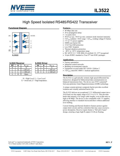
IL3522 High Speed Isolated RS485/RS422 ... - NVE Corporation
IL3522 High Speed Isolated RS485/RS422 ... - NVE Corporation
IL3522 High Speed Isolated RS485/RS422 ... - NVE Corporation

Create successful ePaper yourself
Turn your PDF publications into a flip-book with our unique Google optimized e-Paper software.
<strong>IL3522</strong><br />
<strong>High</strong> <strong>Speed</strong> <strong>Isolated</strong> <strong>RS485</strong>/<strong>RS422</strong> Transceiver<br />
Functional Diagram<br />
DE<br />
D<br />
R<br />
RE<br />
<strong>IL3522</strong><br />
ISODE<br />
Y<br />
Z<br />
A<br />
B<br />
Features<br />
• 40 Mbps data rate<br />
• 20 ns propagation delay<br />
• 1 ns pulse skew<br />
• 50 kV/μs typ.; 30 kV/μs min. common mode transient immunity<br />
• 5 kV RMS isolation / 10 kV surge / 1 kV RMS working voltage (V-Series)<br />
• 3 V to 5 V power supplies<br />
• 44000 year barrier life<br />
• 15 kV bus ESD protection<br />
• Low EMC footprint<br />
• Thermal shutdown protection<br />
• −40°C to +85°C temperature range<br />
• IEC 60747-5-5 / VDE 0884-10 certified; UL 1577 recognized<br />
• 16-pin JEDEC-standard or True 8 mm SOIC packages<br />
<strong>IL3522</strong> Receiver<br />
RE R V (A−B)<br />
H Z X<br />
L H ≥ 200 mV<br />
L L ≤−200 mV<br />
L H Open<br />
<strong>IL3522</strong> Driver<br />
DE D V (Y−Z)<br />
L X Z<br />
H H ≥ 200 mV<br />
H L ≤−200 mV<br />
H = <strong>High</strong> Level, L = Low Level<br />
X = Irrelevant, Z = <strong>High</strong> Impedance<br />
Applications<br />
• Factory automation<br />
• Industrial control networks<br />
• Building environmental controls<br />
• Equipment covered under IEC 61010-1 Edition 3<br />
• 5 kV RMS rated IEC 60601-1 medical applications<br />
Description<br />
The <strong>IL3522</strong> is a galvanically isolated, high-speed differential bus<br />
transceiver, designed for bidirectional data communication on<br />
balanced transmission lines. The device uses <strong>NVE</strong>’s patented*<br />
IsoLoop spintronic Giant Magnetoresistance (GMR) technology.<br />
A unique ceramic/polymer composite barrier provides excellent<br />
isolation and virtually unlimited barrier life.<br />
The <strong>IL3522</strong> delivers an exceptional 2.3 V differential output into a<br />
54 Ω load over the supply range of 4.5 V to 5.5 V. This provides<br />
better data integrity over longer cable lengths, even at data rates as<br />
high as 40 Mbps. The device is also compatible with 3 V supplies,<br />
allowing interface to standard microcontrollers without additional<br />
level shifting.<br />
Current limiting and thermal shutdown features protect against<br />
output short circuits and bus contention that may cause excessive<br />
power dissipation. Receiver inputs feature a “fail-safe if open”<br />
design, ensuring a logic high R-output if A/B are floating.<br />
IsoLoop ® is a registered trademark of <strong>NVE</strong> <strong>Corporation</strong>.<br />
*U.S. Patent number 5,831,426; 6,300,617 and others.<br />
REV. P<br />
<strong>NVE</strong> <strong>Corporation</strong> 11409 Valley View Road, Eden Prairie, MN 55344-3617 Phone: (952) 829-9217 Fax: (952) 829-9189 www.IsoLoop.com ©<strong>NVE</strong> <strong>Corporation</strong>
<strong>IL3522</strong><br />
Absolute Maximum Ratings (11)<br />
Parameters Symbol Min. Typ. Max. Units Test Conditions<br />
Storage Temperature T S −55 150 °C<br />
Ambient Operating Temperature T A −40 85 °C<br />
Voltage Range at any Bus Pin −7 12 V<br />
Supply Voltage (1) V DD1 , V DD2 −0.5 7 V<br />
Digital Input Voltage −0.5 V DD + 0.5 V<br />
Digital Output Voltage −0.5 V DD + 1 V<br />
ESD (all bus nodes) 15 kV HBM<br />
Recommended Operating Conditions<br />
Parameters Symbol Min. Typ. Max. Units Test Conditions<br />
V<br />
Supply Voltage<br />
DD1<br />
3.0<br />
5.5<br />
V<br />
V DD2<br />
4.5<br />
5.5<br />
Input Voltage at any Bus Terminal<br />
12<br />
V<br />
(separately or common mode)<br />
−7<br />
V I<br />
V IC<br />
<strong>High</strong>-Level Digital Input Voltage<br />
V IH<br />
2.4<br />
3.0<br />
V DD1 V<br />
Low-Level Digital Input Voltage V IL 0 0.8 V<br />
Differential Input Voltage (2) V ID +12/−7 V<br />
<strong>High</strong>-Level Output Current (Driver) I OH 60 mA<br />
<strong>High</strong>-Level Digital Output Current<br />
(Receiver)<br />
I OH 8 mA<br />
Low-Level Output Current (Driver) I OL −60 mA<br />
Low-Level Digital Output Current<br />
(Receiver)<br />
I OL −8 mA<br />
Ambient Operating Temperature T A −40 85 °C<br />
Digital Input Signal Rise and Fall<br />
Times<br />
t IR , t IF<br />
DC Stable<br />
V DD1 = 3.3 V<br />
V DD1 = 5.0 V<br />
2<br />
<strong>NVE</strong> <strong>Corporation</strong> 11409 Valley View Road, Eden Prairie, MN 55344-3617 Phone: (952) 829-9217 Fax: (952) 829-9189 www.IsoLoop.com ©<strong>NVE</strong> <strong>Corporation</strong>
<strong>IL3522</strong><br />
Insulation Specifications<br />
Parameters Symbol Min. Typ. Max. Units Test Conditions<br />
Creepage Distance (external) 8.03 8.3 mm Per IEC 60601<br />
Total Barrier Thickness (internal) 0.013 0.014 mm<br />
Barrier Resistance R IO >10 14 Ω 500 V<br />
Barrier Capacitance C IO 7 pF f = 1 MHz<br />
Leakage Current 0.2 μA RMS 240 V RMS , 60 Hz<br />
Comparative Tracking Index CTI ≥175 V Per IEC 60112<br />
<strong>High</strong> Voltage Endurance<br />
(Maximum Barrier Voltage<br />
for Indefinite Life)<br />
AC<br />
DC<br />
V IO<br />
Barrier Life 44000 Years<br />
1000<br />
1500<br />
V RMS<br />
V DC<br />
At maximum<br />
operating temperature<br />
100°C, 1000 V RMS , 60%<br />
CL activation energy<br />
Safety and Approvals<br />
IEC 60747-5-5 (VDE 0884) (Standard isolation grade; File Number 5016933-4880-0001)<br />
• Working Voltage (V IORM ) 600 V RMS (848 V PK ); basic insulation; pollution degree 2<br />
• Transient overvoltage (V IOTM ) and surge voltage (V IOSM ) 4000 V PK<br />
• Each part tested at 1590 V PK for 1 second, 5 pC partial discharge limit<br />
• Samples tested at 4000 V PK for 60 sec.; then 1358 V PK for 10 sec. with 5 pC partial discharge limit<br />
VDE 0884-10 (V-Series isolation grade; certification pending)<br />
• Working Voltage (V IORM ) 1000 V RMS (1415 V PK ); basic insulation; pollution degree 2<br />
• Transient overvoltage (V IOTM ) 6000 V PK<br />
• Surge voltage (V IOSM ) 10 kV PK<br />
• Each part tested at 2387 V PK for 1 second, 5 pC partial discharge limit<br />
• Samples tested at 6000 V PK for 60 sec.; then 2122 V PK for 10 sec. with 5 pC partial discharge limit<br />
IEC 61010-1 (Edition 2; TUV Certificate Numbers N1502812; N1502812-101)<br />
Reinforced Insulation; Pollution Degree II; Material Group III<br />
Part No. Suffix Package Working Voltage<br />
-3 SOIC 150 V RMS<br />
None Wide-body SOIC/True 8 300 V RMS<br />
UL 1577 (Component Recognition Program File Number E207481)<br />
Standard isolation grade<br />
Each part tested at 3000 V RMS (4243 V PK ) for 1 second; each lot sample tested at 2500 V RMS (3536 V PK ) for 1 minute<br />
V-Series isolation grade (recognition pending)<br />
Each part tested at 6000 V RMS (8486 V PK ) for 1 second; each lot sample tested at 5000 V RMS (7072 V PK ) for 1 minute<br />
Soldering Profile<br />
Per JEDEC J-STD-020C, MSL 1<br />
3<br />
<strong>NVE</strong> <strong>Corporation</strong> 11409 Valley View Road, Eden Prairie, MN 55344-3617 Phone: (952) 829-9217 Fax: (952) 829-9189 www.IsoLoop.com ©<strong>NVE</strong> <strong>Corporation</strong>
<strong>IL3522</strong><br />
<strong>IL3522</strong> Pin Connections<br />
1 V DD1 Input Power Supply<br />
Input Power Supply Ground Return<br />
2 GND 1<br />
(pin 2 is internally connected to pin 8)<br />
3 R Output Data from Bus<br />
4 RE<br />
Read Data Enable<br />
(if RE is high, R = high impedance)<br />
5 DE Drive Enable<br />
6 D Data Input to Bus<br />
7 NC No Internal Connection<br />
Input Power Supply Ground Return<br />
8 GND 1<br />
(pin 8 is internally connected to pin 2)<br />
Output Power Supply Ground Return<br />
9 GND 2<br />
(pin 9 is internally connected to pin 15)<br />
<strong>Isolated</strong> DE Output for use in Profibus<br />
10 ISODE applications where the state of the isolated<br />
drive enable node needs to be monitored<br />
11 Y Y Bus (Drive – True)<br />
12 Z Z Bus (Drive – Inverse)<br />
13 B B Bus (Receive – Inverse)<br />
14 A A Bus (Receive – True)<br />
Output Power Supply Ground Return<br />
15 GND 2<br />
(pin 15 is internally connected to pin 9)<br />
16 V DD2 Output Power Supply<br />
VDD 1<br />
VDD 2<br />
GND 1<br />
GND 2<br />
R<br />
A<br />
RE<br />
B<br />
DE<br />
Z<br />
D<br />
NC<br />
Y<br />
ISODE<br />
GND 1<br />
GND 2<br />
<strong>IL3522</strong><br />
4<br />
<strong>NVE</strong> <strong>Corporation</strong> 11409 Valley View Road, Eden Prairie, MN 55344-3617 Phone: (952) 829-9217 Fax: (952) 829-9189 www.IsoLoop.com ©<strong>NVE</strong> <strong>Corporation</strong>
<strong>IL3522</strong><br />
Driver Section<br />
Electrical Specifications are T min to T max and V DD = 4.5 V to 5.5 V, unless otherwise stated.<br />
Parameters Symbol Min. Typ. (5) Max. Units Test Conditions<br />
Input Clamp Voltage V IK −1.5 V I L = −18 mA<br />
Output voltage V O V DD V I O = 0<br />
Differential Output Voltage (12) |V OD1 | V DD V I O = 0<br />
Differential Output Voltage (12) |V OD2 | 2.5 3 5 V R L = 54 Ω, V DD = 5 V<br />
Differential Output Voltage (12, 6) V OD3 2.3 5 V R L = 54 Ω, V DD = 4.5 V<br />
Change in Magnitude of Differential<br />
Output Voltage (7) Δ|V OD | ±0.2 V R L = 54 Ω or 100 Ω<br />
Common Mode Output Voltage V OC 3 V R L = 54 Ω or 100 Ω<br />
Change in Magnitude of Common<br />
Mode Output Voltage (7) Δ|V OC | ±0.2 V R L = 54 Ω or 100 Ω<br />
1<br />
Output Current (4)<br />
I O<br />
−0.8<br />
<strong>High</strong> Level Input Current I IH 10 μA V I = 3.5 V<br />
Low Level Input Current I IL −10 μA V I = 0.4 V<br />
Absolute |Short-circuit Output<br />
Current|<br />
Supply Current<br />
V DD1 = +5 V<br />
V DD1 = +3.3 V<br />
mA<br />
Output Disabled, V O = 12<br />
V O = −7<br />
I OS 250 mA −7 V > V O < 12 V<br />
I DD1<br />
I DD1<br />
4<br />
3<br />
6<br />
4<br />
mA<br />
No Load<br />
(Outputs Enabled)<br />
Notes (apply to both driver and receiver sections):<br />
1. All voltages are with respect to network ground except differential I/O bus voltages.<br />
2. Differential input voltage is measured at the noninverting terminal A with respect to the inverting terminal B.<br />
3. Skew limit is the maximum propagation delay difference between any two devices at 25°C.<br />
4. The power-off measurement in ANSI Standard EIA/TIA-422-B applies to disabled outputs only and is not applied to combined inputs and<br />
outputs.<br />
5. All typical values are at V DD1 ,V DD2 = 5 V or V DD1 = 3.3 V and T A = 25°C.<br />
6. −7 V < V CM < 12 V; 4.5 V < V DD < 5.5 V.<br />
7. Δ|V OD | and Δ|V OC | are the changes in magnitude of V OD and V OC , respectively, that occur when the input is changed from one logic state to<br />
the other.<br />
8. This applies for both power on and power off, refer to ANSI standard RS-485 for exact condition. The EIA/TIA-422-B limit does not apply<br />
for a combined driver and receiver terminal.<br />
9. Includes 10 ns read enable time. Maximum propagation delay is 25 ns after read assertion.<br />
10. Pulse skew is defined as |t PLH – t PHL | of each channel.<br />
11. Absolute Maximum specifications mean the device will not be damaged if operated under these conditions. It does not guarantee<br />
performance.<br />
12. Differential output voltage is measured at terminal Y with respect to Z.<br />
13. The relevant test and measurement methods are given in the Electromagnetic Compatibility section on p. 6.<br />
14. External magnetic field immunity is improved by this factor if the field direction is “end-to-end” rather than to “pin-to-pin” (see diagram on p. 6).<br />
5<br />
<strong>NVE</strong> <strong>Corporation</strong> 11409 Valley View Road, Eden Prairie, MN 55344-3617 Phone: (952) 829-9217 Fax: (952) 829-9189 www.IsoLoop.com ©<strong>NVE</strong> <strong>Corporation</strong>
<strong>IL3522</strong><br />
Receiver Section<br />
Electrical Specifications (T min to T max and V DD = 4.5 V to 5.5 V unless otherwise stated)<br />
Parameters Symbol Min. Typ. (5) Max. Units Test Conditions<br />
Positive-going Input Threshold<br />
Voltage (2) V IT+ 0.2 V −7 V > V CM < 12 V<br />
Negative-going Input Threshold<br />
Voltage (2) V IT- −0.2 V −7 V > V CM < 12 V<br />
Hysteresis Voltage (V IT+ − V IT- ) V HYS 40 mV V CM = 0 V, T = 25°C<br />
<strong>High</strong> Level Digital Output Voltage V OH V DD – 0.2 V DD V<br />
V ID = 200 mV<br />
I OH = −20 μA<br />
Low Level Digital Output Voltage V OL 0.2 V<br />
V ID = −200 mV<br />
I OH = 20 μA<br />
<strong>High</strong>-impedance-state output current I OZ ±1 μA V O =0.4 to (V DD2 −0.5) V<br />
Line Input Current (8) I I 1 mA V I = 12 V<br />
−0.8 mA V I = −7 V<br />
Input Resistance R I 20 kΩ<br />
Supply Current I DD2 5 16 mA<br />
No load<br />
(Outputs Enabled)<br />
Switching Characteristics<br />
V DD1 = 5 V, V DD2 = 5 V<br />
Parameters Symbol Min. Typ. (5) Max. Units Test Conditions<br />
Data Rate 40 Mbps R L = 54 Ω, C L = 50 pF<br />
Propagation Delay (2, 9) t PD 27 35 ns<br />
V O = −1.5 to 1.5 V,<br />
C L = 15 pF<br />
Pulse Skew (2, 10) t SK (P) 1 6 ns<br />
V O = −1.5 to 1.5 V,<br />
C L = 15 pF<br />
Skew Limit (3) t SK (LIM) 2 12 ns R L = 54 Ω, C L = 50 pF<br />
Output Enable Time To <strong>High</strong> Level t PZH 15 25 ns C L = 15 pF<br />
Output Enable Time To Low Level t PZL 15 25 ns C L = 15 pF<br />
Output Disable Time From <strong>High</strong><br />
Level<br />
t PHZ 15 25 ns C L = 15 pF<br />
Output Disable Time From Low Level t PLZ 15 25 ns C L = 15 pF<br />
Common Mode Transient Immunity<br />
|CM<br />
(Output Logic <strong>High</strong> to Logic Low)<br />
H |,|CM L | 30 50 kV/μs<br />
V CM = 1500 V DC<br />
t TRANSIENT = 25 ns<br />
V DD1 = 3.3 V, V DD2 = 5 V<br />
Parameters Symbol Min. Typ. (5) Max. Units Test Conditions<br />
Data Rate 40 Mbps R L = 54 Ω, C L = 50 pF<br />
Propagation Delay (2, 9) t PD 30 38 ns<br />
Pulse Skew (2, 10) t SK (P) 1 6 ns<br />
V O = −1.5 to 1.5 V,<br />
C L = 15 pF<br />
V O = −1.5 to 1.5 V,<br />
C L = 15 pF<br />
Skew Limit (3) t SK (LIM) 4 12 ns R L = 54 Ω, C L = 50 pF<br />
Output Enable Time To <strong>High</strong> Level t PZH 17 27 ns C L = 15 pF<br />
Output Enable Time To Low Level t PZL 17 27 ns C L = 15 pF<br />
Output Disable Time From <strong>High</strong><br />
Level<br />
t PHZ 17 27 ns C L = 15 pF<br />
Output Disable Time From Low Level t PLZ 17 27 ns C L = 15 pF<br />
Common Mode Transient Immunity<br />
(Output Logic <strong>High</strong> to Logic Low)<br />
|CM H |,|CM L | 30 50 kV/μs<br />
V CM = 1500 V DC<br />
t TRANSIENT = 25 ns<br />
6<br />
<strong>NVE</strong> <strong>Corporation</strong> 11409 Valley View Road, Eden Prairie, MN 55344-3617 Phone: (952) 829-9217 Fax: (952) 829-9189 www.IsoLoop.com ©<strong>NVE</strong> <strong>Corporation</strong>
<strong>IL3522</strong><br />
Magnetic Field Immunity (13)<br />
V DD1 = 5 V, V DD2 = 5 V<br />
Power Frequency Magnetic Immunity H PF 2800 3500 A/m 50Hz/60Hz<br />
Pulse Magnetic Field Immunity H PM 4000 4500 A/m t p = 8µs<br />
Damped Oscillatory Magnetic Field H OSC 4000 4500 A/m 0.1Hz – 1MHz<br />
Cross-axis Immunity Multiplier (14) K X 2.5<br />
V DD1 = 3.3 V, V DD2 = 5 V<br />
Power Frequency Magnetic Immunity H PF 1000 1500 A/m 50Hz/60Hz<br />
Pulse Magnetic Field Immunity H PM 1800 2000 A/m t p = 8µs<br />
Damped Oscillatory Magnetic Field H OSC 1800 2000 A/m 0.1Hz – 1MHz<br />
Cross-axis Immunity Multiplier (14) K X 2.5<br />
7<br />
<strong>NVE</strong> <strong>Corporation</strong> 11409 Valley View Road, Eden Prairie, MN 55344-3617 Phone: (952) 829-9217 Fax: (952) 829-9189 www.IsoLoop.com ©<strong>NVE</strong> <strong>Corporation</strong>
<strong>IL3522</strong><br />
Electrostatic Discharge Sensitivity<br />
This product has been tested for electrostatic sensitivity to the limits stated in the specifications. However, <strong>NVE</strong> recommends that all integrated<br />
circuits be handled with appropriate care to avoid damage. Damage caused by inappropriate handling or storage could range from performance<br />
degradation to complete failure.<br />
Power Consumption<br />
IsoLoop Isolators achieve their low power consumption from the way they transmit data across the isolation barrier. By detecting the edge<br />
transitions of the input logic signal and converting these to narrow current pulses, a magnetic field is created around the GMR Wheatstone<br />
bridge. Depending on the direction of the magnetic field, the bridge causes the output comparator to switch following the input logic signal.<br />
Since the current pulses are narrow, about 2.5 ns, the power consumption is independent of mark-to-space ratio and solely dependent on<br />
frequency. This has obvious advantages over optocouplers, which have power consumption heavily dependent on frequency and time.<br />
Power Supply Decoupling<br />
Data Rate (Mbps) I DD1 I DD2<br />
1 100 μA 100 μA<br />
10 1 mA 1 mA<br />
20 2 mA 2 mA<br />
40 4 mA 4 mA<br />
Table 2. Typical Dynamic Supply Currents.<br />
Both V DD1 and V DD2 must be bypassed with 47 nF ceramic capacitors. These should be placed as close as possible to V DD pins for proper<br />
operation. Additionally, V DD2 should be bypassed with a 10 µF tantalum capacitor.<br />
Maintaining Creepage<br />
Creepage distances are often critical in isolated circuits. In addition to meeting JEDEC standards, <strong>NVE</strong> isolator packages have unique creepage<br />
specifications. Standard pad libraries often extend under the package, compromising creepage and clearance. Similarly, ground planes, if used,<br />
should be spaced to avoid compromising clearance. Package drawings and recommended pad layouts are included in this datasheet.<br />
DC Correctness<br />
The <strong>IL3522</strong> incorporates a patented refresh circuit to maintain the correct output state with respect to data input. At power up, the bus outputs<br />
will follow the Function Table shown on Page 1. The DE input should be held low during power-up to eliminate false drive data pulses from the<br />
bus. An external power supply monitor to minimize glitches caused by slow power-up and power-down transients is not required.<br />
Electromagnetic Compatibility<br />
The <strong>IL3522</strong> is fully compliant with generic EMC standards EN50081, EN50082-1 and the umbrella line-voltage standard for Information<br />
Technology Equipment (ITE) EN61000. The IsoLoop Isolator’s Wheatstone bridge configuration and differential magnetic field signaling ensure<br />
excellent EMC performance against all relevant standards. <strong>NVE</strong> conducted compliance tests in the categories below:<br />
EN50081-1<br />
Residential, Commercial & Light Industrial<br />
Methods EN55022, EN55014<br />
EN50082-2: Industrial Environment<br />
Methods EN61000-4-2 (ESD), EN61000-4-3 (Electromagnetic Field Immunity), EN61000-4-4 (Electrical Transient Immunity),<br />
EN61000-4-6 (RFI Immunity), EN61000-4-8 (Power Frequency Magnetic Field Immunity), EN61000-4-9 (Pulsed Magnetic<br />
Field), EN61000-4-10 (Damped Oscillatory Magnetic Field)<br />
ENV50204<br />
Radiated Field from Digital Telephones (Immunity Test)<br />
Immunity to external magnetic fields is even higher if the field direction is “end-to-end” (rather than to “pin-to-pin”) as shown in<br />
the diagram at right.<br />
8<br />
<strong>NVE</strong> <strong>Corporation</strong> 11409 Valley View Road, Eden Prairie, MN 55344-3617 Phone: (952) 829-9217 Fax: (952) 829-9189 www.IsoLoop.com ©<strong>NVE</strong> <strong>Corporation</strong>
<strong>IL3522</strong><br />
Application Information<br />
The following figure shows typical connections to a microcontroller. The schematic includes typical termination and fail-safe resistors, and<br />
power supply decoupling capacitors:<br />
VDD1 = 3.3 V<br />
VDD2 = 5 V<br />
C DD1<br />
47nF<br />
1<br />
<strong>IL3522</strong><br />
16<br />
C DD2B<br />
C DD2 +<br />
47nF 10µF<br />
Microcontroller<br />
DE<br />
D<br />
R<br />
RE<br />
5<br />
6<br />
3<br />
4<br />
10<br />
ISODE R FS-EXT<br />
560R<br />
11<br />
12<br />
13<br />
14 R T<br />
120R<br />
Y<br />
Z<br />
A<br />
B<br />
2 or 8 9 or 15<br />
GND1<br />
Isolation<br />
Boundary<br />
GND2<br />
R FS-EXT<br />
560R<br />
Typical <strong>IL3522</strong> connections.<br />
Receiver Features<br />
The receiver includes a “fail-safe if open” function that guarantees a high level output if the receiver inputs are unconnected (floating). The<br />
receiver output “R” has tri-state capability via the active low RE input.<br />
Driver Features<br />
The RS-422 driver is differential output and delivers at least 1.5 V across a 54 Ω load. Drivers feature low propagation delay skew to maximize<br />
bit width and minimize EMI. Drivers have tri-state capability via the active-high DE input.<br />
Receiver Data Rate, Cables and Terminations<br />
The <strong>IL3522</strong> is intended for networks up to 4,000 feet (1,200 m), but the maximum data rate decreases as cable length increases. Twisted pair<br />
cable should be used in all networks since they tend to pick up noise and other electromagnetically induced voltages as common mode signals,<br />
which are effectively rejected by the differential receivers.<br />
9<br />
<strong>NVE</strong> <strong>Corporation</strong> 11409 Valley View Road, Eden Prairie, MN 55344-3617 Phone: (952) 829-9217 Fax: (952) 829-9189 www.IsoLoop.com ©<strong>NVE</strong> <strong>Corporation</strong>
<strong>IL3522</strong><br />
Fail-Safe Operation<br />
“Fail-safe operation” is defined here as the forcing of a logic high state on the “R” output in response to an open-circuit condition between the<br />
“A” and “B” lines of the bus, or when no drivers are active on the bus.<br />
Proper biasing can ensure fail-safe operation, that is a known state when there are no active drivers on the bus. IL3000-Series <strong>Isolated</strong><br />
Transceivers include internal pull-up and pull-down resistors of approximately 30 kΩ in the receiver section (R FS-INT ; see figure below). These<br />
internal resistors are designed to ensure failsafe operation but only if there are no termination resistors. The entire V DD will appear between inputs<br />
“A” and “B” if there is no loading and no termination resistors, and there will be more than the required 200 mV with up to four RS-422 worstcase<br />
Unit Loads of 12 kΩ. Many designs operating below 1 Mbps or less than 1,000 feet are unterminated. Termination resistors may not be<br />
necessary for very low data rates and very short cable runs because reflections have time to settle before data sampling, which occurs at the<br />
middle of the bit interval.<br />
In busses with low-impedance termination resistors, however, the differential voltage across the conductor pair will be close to zero with no<br />
active drivers. In this case the state of the bus is indeterminate, and the idle bus will be susceptible to noise. For example, with 120 Ω termination<br />
resistors (R T ) on each end of the cable, and four Unit Loads (12 kΩ each), without external fail-safe biasing resistors the internal pull-up and pulldown<br />
resistors will produce a voltage between inputs “A” and “B” of only about 5 mV. This is not nearly enough to ensure a known state.<br />
External fail-safe biasing resistors (R FS-EXT ) at one end of the bus can ensure fail-safe operation with a terminated bus. Resistors should be<br />
selected so that under worst-case power supply and resistor tolerances there is at least 200 mV across the conductor pair with no active drivers to<br />
meet the input sensitivity specification of the RS-422 standard.<br />
Using the same value for pull-up and pull-down biasing resistors maintains balance for positive- and negative going transitions. Lower-value<br />
resistors increase inactive noise immunity at the expense of quiescent power consumption. Note that each Unit Load on the bus adds a worst-case<br />
loading of 12 kΩ across the conductor pair, and 32 Unit Loads add 375 Ω worst-case loading. The more loads on the bus, the lower the required<br />
values of the biasing resistors.<br />
In the example with two 120 Ω termination resistors and four Unit Loads, 560 Ω external biasing resistors provide more than 200 mV between<br />
“A” and “B” with adequate margin for power supply variations and resistor tolerances. This ensures a known state when there are no active<br />
drivers. Other illustrative examples are shown in the table below:<br />
Fail-Safe Biasing<br />
5 V<br />
R<br />
V DD<br />
RFS-INT RFS-INT<br />
GND<br />
30K 30K<br />
A<br />
B<br />
RFS-EXT<br />
RFS-EXT<br />
RT<br />
RT<br />
R FS-EXT R T<br />
Nominal V A-B Fail-Safe<br />
Loading (inactive) Operation?<br />
Internal Only None Four unit loads (12 kΩ ea.) 238 mV Yes<br />
Internal Only 120 Ω Four unit loads (12 kΩ ea.) 5 mV No<br />
560 Ω 120 Ω Four unit loads (12 kΩ ea.) 254 mV Yes<br />
510 Ω 120 Ω 32 unit loads (12 kΩ ea.) 247 mV Yes<br />
10<br />
<strong>NVE</strong> <strong>Corporation</strong> 11409 Valley View Road, Eden Prairie, MN 55344-3617 Phone: (952) 829-9217 Fax: (952) 829-9189 www.IsoLoop.com ©<strong>NVE</strong> <strong>Corporation</strong>
<strong>IL3522</strong><br />
Package Drawing<br />
0.3" 16-pin SOIC Package<br />
Dimensions in inches (mm); scale = approx. 5X<br />
0.033 (0.85)*<br />
0.043 (1.10)<br />
0.260 (6.60)*<br />
0.280 (7.11)<br />
0.013 (0.3)<br />
0.020 (0.5)<br />
0.397 (10.08)<br />
0.413 (10.49)<br />
0.007 (0.2)<br />
0.013 (0.3)<br />
0.007 (0.18)*<br />
0.010 (0.25)<br />
0.016 (0.4)<br />
0.050 (1.3)<br />
0.017 (0.43)*<br />
0.022 (0.56)<br />
Pin 1 identified by<br />
either an indent<br />
or a marked dot<br />
0.08 (2.0)<br />
0.10 (2.5)<br />
0.092 (2.34)<br />
0.105 (2.67)<br />
0.292 (7.42)*<br />
0.299 (7.59)<br />
0.394 (10.00)<br />
0.419 (10.64)<br />
*Specified for True 8 package to guarantee 8 mm creepage per IEC 60601.<br />
0.049 (1.24)<br />
0.051 (1.30)<br />
NOTE: Pin spacing is a BASIC<br />
dimension; tolerances<br />
do not accumulate<br />
0.004 (0.1)<br />
0.012 (0.3)<br />
Recommended Pad Layout<br />
0.15" 16-pin SOIC Pad Layout<br />
Dimensions in inches (mm); scale = approx. 5X<br />
0.317 (8.05)<br />
0.050 (1.27)<br />
0.020 (0.51)<br />
16 PLCS<br />
0.449 (11.40)<br />
11<br />
<strong>NVE</strong> <strong>Corporation</strong> 11409 Valley View Road, Eden Prairie, MN 55344-3617 Phone: (952) 829-9217 Fax: (952) 829-9189 www.IsoLoop.com ©<strong>NVE</strong> <strong>Corporation</strong>
<strong>IL3522</strong><br />
Ordering Information and Valid part Numbers<br />
IL 35 22 V E TR13<br />
Bulk Packaging<br />
Blank = Tube<br />
TR13 = 13'' Tape and Reel<br />
Package<br />
Blank = 80/20 Sn/Pb Plating<br />
E = RoHS Compliant<br />
Isolation Grade<br />
Blank = 2.5 kV Isolation / 600 WV<br />
V = 5 kV Isolation / 1 kV WV<br />
Valid Part Numbers<br />
<strong>IL3522</strong><br />
<strong>IL3522</strong>E<br />
<strong>IL3522</strong>TR13<br />
<strong>IL3522</strong>E TR13<br />
<strong>IL3522</strong>VE<br />
<strong>IL3522</strong>VE TR13<br />
Channel Configuration<br />
22 = RS-422<br />
Base Part Number<br />
35 = Digital-In, 40 Mbps Transceiver<br />
Product Family<br />
IL = Isolators<br />
RoHS<br />
COMPLIANT<br />
12<br />
<strong>NVE</strong> <strong>Corporation</strong> 11409 Valley View Road, Eden Prairie, MN 55344-3617 Phone: (952) 829-9217 Fax: (952) 829-9189 www.IsoLoop.com ©<strong>NVE</strong> <strong>Corporation</strong>
<strong>IL3522</strong><br />
Revision History<br />
ISB-DS-001-<strong>IL3522</strong>-P<br />
August 2014<br />
• Increase V-Series surge voltage specification to 10 kV.<br />
• Upgraded V-Series safety and approval from IEC 60747-5-5 (VDE 0884) to VDE 0884-10.<br />
ISB-DS-001-<strong>IL3522</strong>-O • Added V-Series versions (5 kVrms isolation / 1000 Vrms working voltage).<br />
ISB-DS-001-<strong>IL3522</strong>-N • IEC 60747-5-5 (VDE 0884) certification.<br />
• Upgraded from MSL 2 to MSL 1.<br />
ISB-DS-001-<strong>IL3522</strong>-M • Increased transient immunity specifications based on additional data.<br />
• Added VDE 0884 pending.<br />
• Added transient immunity specifications.<br />
• Added high voltage endurance specification.<br />
• Increased magnetic immunity specifications.<br />
• Updated package drawings.<br />
• Added recommended solder pad layouts.<br />
ISB-DS-001-<strong>IL3522</strong>-L • Changed title to “Very <strong>High</strong> <strong>Speed</strong> <strong>Isolated</strong> <strong>RS485</strong>/<strong>RS422</strong> Transceiver.”<br />
• Detailed isolation and barrier specifications.<br />
• Cosmetic changes.<br />
ISB-DS-001-<strong>IL3522</strong>-K • Update terms and conditions.<br />
ISB-DS-001-<strong>IL3522</strong>-J • Added clarification of internal ground connections (p. 3).<br />
ISB-DS-001-<strong>IL3522</strong>-I • Revised maximum Receiver Section Supply Current to 16 mA.<br />
ISB-DS-001-<strong>IL3522</strong>-H • Added low EMC footprint.<br />
ISB-DS-001-<strong>IL3522</strong>-G • Added bus-protection ESD specification (15 kV).<br />
ISB-DS-001-<strong>IL3522</strong>-F • Added magnetic field immunity and electromagnetic compatibility specifications.<br />
• Added note on package drawing that pin-spacing tolerances are non-accumulating.<br />
ISB-DS-001-<strong>IL3522</strong>-E • Changed ordering information to reflect that devices are now fully RoHS compliant<br />
with no exemptions.<br />
ISB-DS-001-<strong>IL3522</strong>-C • Eliminated soldering profile chart<br />
13<br />
<strong>NVE</strong> <strong>Corporation</strong> 11409 Valley View Road, Eden Prairie, MN 55344-3617 Phone: (952) 829-9217 Fax: (952) 829-9189 www.IsoLoop.com ©<strong>NVE</strong> <strong>Corporation</strong>
<strong>IL3522</strong><br />
Datasheet Limitations<br />
The information and data provided in datasheets shall define the specification of the product as agreed between <strong>NVE</strong> and its customer, unless <strong>NVE</strong> and<br />
customer have explicitly agreed otherwise in writing. All specifications are based on <strong>NVE</strong> test protocols. In no event however, shall an agreement be<br />
valid in which the <strong>NVE</strong> product is deemed to offer functions and qualities beyond those described in the datasheet.<br />
Limited Warranty and Liability<br />
Information in this document is believed to be accurate and reliable. However, <strong>NVE</strong> does not give any representations or warranties, expressed or<br />
implied, as to the accuracy or completeness of such information and shall have no liability for the consequences of use of such information.<br />
In no event shall <strong>NVE</strong> be liable for any indirect, incidental, punitive, special or consequential damages (including, without limitation, lost profits, lost<br />
savings, business interruption, costs related to the removal or replacement of any products or rework charges) whether or not such damages are based on<br />
tort (including negligence), warranty, breach of contract or any other legal theory.<br />
Right to Make Changes<br />
<strong>NVE</strong> reserves the right to make changes to information published in this document including, without limitation, specifications and product descriptions<br />
at any time and without notice. This document supersedes and replaces all information supplied prior to its publication.<br />
Use in Life-Critical or Safety-Critical Applications<br />
Unless <strong>NVE</strong> and a customer explicitly agree otherwise in writing, <strong>NVE</strong> products are not designed, authorized or warranted to be suitable for use in life<br />
support, life-critical or safety-critical devices or equipment. <strong>NVE</strong> accepts no liability for inclusion or use of <strong>NVE</strong> products in such applications and such<br />
inclusion or use is at the customer’s own risk. Should the customer use <strong>NVE</strong> products for such application whether authorized by <strong>NVE</strong> or not, the<br />
customer shall indemnify and hold <strong>NVE</strong> harmless against all claims and damages.<br />
Applications<br />
Applications described in this datasheet are illustrative only. <strong>NVE</strong> makes no representation or warranty that such applications will be suitable for the<br />
specified use without further testing or modification.<br />
Customers are responsible for the design and operation of their applications and products using <strong>NVE</strong> products, and <strong>NVE</strong> accepts no liability for any<br />
assistance with applications or customer product design. It is customer’s sole responsibility to determine whether the <strong>NVE</strong> product is suitable and fit for<br />
the customer’s applications and products planned, as well as for the planned application and use of customer’s third party customers. Customers should<br />
provide appropriate design and operating safeguards to minimize the risks associated with their applications and products.<br />
<strong>NVE</strong> does not accept any liability related to any default, damage, costs or problem which is based on any weakness or default in the customer’s<br />
applications or products, or the application or use by customer’s third party customers. The customer is responsible for all necessary testing for the<br />
customer’s applications and products using <strong>NVE</strong> products in order to avoid a default of the applications and the products or of the application or use by<br />
customer’s third party customers. <strong>NVE</strong> accepts no liability in this respect.<br />
Limiting Values<br />
Stress above one or more limiting values (as defined in the Absolute Maximum Ratings System of IEC 60134) will cause permanent damage to the<br />
device. Limiting values are stress ratings only and operation of the device at these or any other conditions above those given in the recommended<br />
operating conditions of the datasheet is not warranted. Constant or repeated exposure to limiting values will permanently and irreversibly affect the<br />
quality and reliability of the device.<br />
Terms and Conditions of Sale<br />
In case an individual agreement is concluded only the terms and conditions of the respective agreement shall apply. <strong>NVE</strong> hereby expressly objects to<br />
applying the customer’s general terms and conditions with regard to the purchase of <strong>NVE</strong> products by customer.<br />
No Offer to Sell or License<br />
Nothing in this document may be interpreted or construed as an offer to sell products that is open for acceptance or the grant, conveyance or implication<br />
of any license under any copyrights, patents or other industrial or intellectual property rights.<br />
Export Control<br />
This document as well as the items described herein may be subject to export control regulations. Export might require a prior authorization from national authorities.<br />
Automotive Qualified Products<br />
Unless the datasheet expressly states that a specific <strong>NVE</strong> product is automotive qualified, the product is not suitable for automotive use. It is neither<br />
qualified nor tested in accordance with automotive testing or application requirements. <strong>NVE</strong> accepts no liability for inclusion or use of non-automotive<br />
qualified products in automotive equipment or applications.<br />
In the event that customer uses the product for design-in and use in automotive applications to automotive specifications and standards, customer (a) shall<br />
use the product without <strong>NVE</strong>’s warranty of the product for such automotive applications, use and specifications, and (b) whenever customer uses the<br />
product for automotive applications beyond <strong>NVE</strong>’s specifications such use shall be solely at customer’s own risk, and (c) customer fully indemnifies<br />
<strong>NVE</strong> for any liability, damages or failed product claims resulting from customer design and use of the product for automotive applications beyond <strong>NVE</strong>’s<br />
standard warranty and <strong>NVE</strong>’s product specifications.<br />
14<br />
<strong>NVE</strong> <strong>Corporation</strong> 11409 Valley View Road, Eden Prairie, MN 55344-3617 Phone: (952) 829-9217 Fax: (952) 829-9189 www.IsoLoop.com ©<strong>NVE</strong> <strong>Corporation</strong>
<strong>IL3522</strong><br />
An ISO 9001 Certified Company<br />
<strong>NVE</strong> <strong>Corporation</strong><br />
11409 Valley View Road<br />
Eden Prairie, MN 55344-3617 USA<br />
Telephone: (952) 829-9217<br />
Fax: (952) 829-9189<br />
www.nve.com<br />
e-mail: iso-info@nve.com<br />
©<strong>NVE</strong> <strong>Corporation</strong><br />
All rights are reserved. Reproduction in whole or in part is prohibited without the prior written consent of the copyright owner.<br />
ISB-DS-001-<strong>IL3522</strong>-P<br />
15<br />
August 2014<br />
<strong>NVE</strong> <strong>Corporation</strong> 11409 Valley View Road, Eden Prairie, MN 55344-3617 Phone: (952) 829-9217 Fax: (952) 829-9189 www.IsoLoop.com ©<strong>NVE</strong> <strong>Corporation</strong>