

Micron ® PISMO ™ Module Data Sheet
Micron ® PISMO ™ Module Data Sheet
Micron ® PISMO ™ Module Data Sheet

Create successful ePaper yourself
Turn your PDF publications into a flip-book with our unique Google optimized e-Paper software.
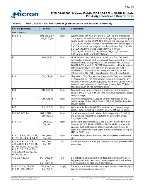
Advance<br />
<strong>PISMO</strong>2-00001: <strong>Micron</strong> Mobile DDR SDRAM + NAND <strong>Module</strong><br />
Pin Assignments and Descriptions<br />
Table 5: <strong>PISMO</strong>2-00001 Ball Descriptions (Referenced to the Bottom Connector)<br />
Ball No. (Bottom) Symbol Type Description<br />
DRAM Section<br />
D12, E12 DM_CLK0_DH Input System clock: DM_CLK_DH and DM_CLK_DL are differential<br />
DM_CLK0_DL<br />
clock inputs. All address and control input signals are sampled<br />
on the positive edge of DM_CLK_DH and the negative edge of<br />
DM_CLK_DL. Output (read) data is referenced to both edges of<br />
DM_CLK. Internal clock signals are derived from DM_CLK_DH/<br />
DM_CLK_DL. SDRAM and Mobile SDRAM only use<br />
DM_CLK_DH. Both DM_CLK_DH and DM_CLK_DL apply to<br />
DDR, Mobile DDR, and DDR2 SDRAM.<br />
E5 DM_CKE0 Input Clock enable: DM_CKE HIGH activates, and DM_CKE LOW<br />
deactivates, internal clock signals and device input buffers and<br />
output drivers. Taking DM_CKE LOW provides PRECHARGE,<br />
POWER-DOWN, and SELF REFRESH operation (all banks idle) or<br />
active power-down (row active in any bank). DM_CKE is<br />
synchronous for power-down entry and exit and for self<br />
refresh entry. DM_CKE is asynchronous for self refresh exit.<br />
E15 DM_CS0_N Input Chip select: DM_CS_N enables (registered LOW) and disables<br />
(registered HIGH) the command decoder. All commands are<br />
masked when DM_CS_N is registered HIGH. DM_CS_N provides<br />
external bank selection on multibank systems. DM_CS_N is<br />
considered part of the command code.<br />
D17 DM_RAS_N Input Row address strobe: Latches row addresses on the positive<br />
edge of the DM_CLK with DM_RAS_N LOW. Enables row access<br />
and precharge.<br />
E17 DM_CAS_N Input Column address strobe: Latches column addresses on the<br />
positive edge of the DM_CLK with DM_CAS_N LOW. Enables<br />
column access.<br />
D15 DM_WE_N Input Write enable: Enables WRITE operation and row precharge.<br />
Latches data in starting from DM_CAS_N, DM_WE_N active.<br />
D16, D8, D20, E6 DM_DQM0 to<br />
DM_DQM3<br />
E18, D18 DM_BA0,<br />
DM_BA1<br />
E19, D19, E14, E20, E2, E8,<br />
E3, D3, D7, E4, D14, D4, E7<br />
B11, A11, B12, A12, B13,<br />
A13, A14, B14, A7, B7, A8,<br />
B8, A9, B9, B10, A10, A16,<br />
B16, B17, A17, B18, B19,<br />
A18, A19, B2, B3, A2, A3,<br />
B4, A4, A5, B5<br />
DM_A0 to<br />
DM_A12<br />
DM_D0 to<br />
DM_D31<br />
A15, A6, A20, A1 DM_DQS0_DH<br />
to<br />
DM_DQS3_DH<br />
C19, C18, C14, C8, C12,<br />
C10, C9, C15, C11, C7<br />
DM_VIO_0 to<br />
DM_VIO_9<br />
Input <strong>Data</strong> input/output mask: Makes data output High-Z, t SHZ after<br />
the clock and masks the output. Blocks data input when<br />
DM_DQM active.<br />
Input Bank select address: DM_BA0 and DM_BA1 define to which<br />
bank an ACTIVE, READ, WRITE, or PRECHARGE command is<br />
applied. Bank address also determines whether the mode<br />
register or extended mode register is to be accessed during an<br />
MRS or EMRS cycle.<br />
Input Address: Row/column addresses are multiplexed on the same<br />
pins.<br />
I/O <strong>Data</strong> input/output: <strong>Data</strong> inputs/outputs are multiplexed on the<br />
same pins.<br />
I/O <strong>Data</strong> strobes: Output with read data, input with write data.<br />
Edge-aligned with read data, center-aligned with write data.<br />
Only applicable to DDR and DDR2 SDRAM.<br />
Supply <strong>Data</strong> output power: Isolates the output buffer power supply to<br />
provide improved noise immunity.<br />
PDF: 09005aef827fda9b/Source: 09005aef827fda71 <strong>Micron</strong> Technology, Inc., reserves the right to change products or specifications without notice.<br />
<strong>PISMO</strong>2_00001_datasheet.fm - Rev. B 11/07 EN 6 ©2007 <strong>Micron</strong> Technology, Inc. All rights reserved.


