You also want an ePaper? Increase the reach of your titles
YUMPU automatically turns print PDFs into web optimized ePapers that Google loves.
<strong>NPMC</strong>-<strong>8E1</strong>/<strong>T1</strong>/<strong>J1</strong> – Technical Reference Manual<br />
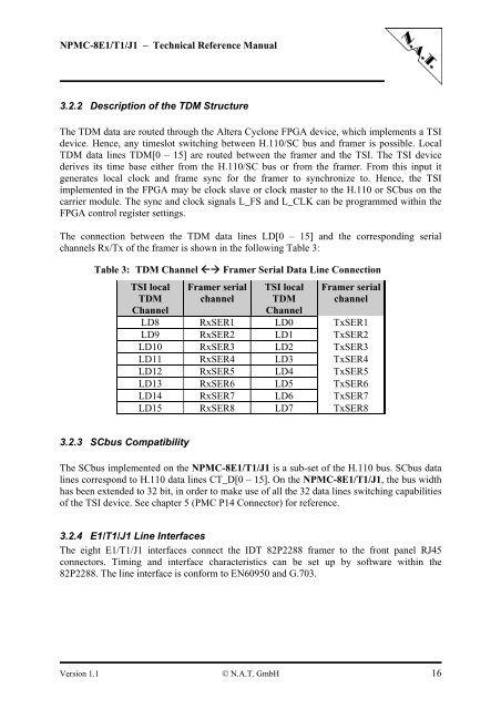
3.2.2 Description of the TDM Structure<br />
The TDM data are routed through the Altera Cyclone FPGA device, which implements a TSI<br />
device. Hence, any timeslot switching between H.110/SC bus and framer is possible. Local<br />
TDM data lines TDM[0 – 15] are routed between the framer and the TSI. The TSI device<br />
derives its time base either from the H.110/SC bus or from the framer. From this input it<br />
generates local clock and frame sync for the framer to synchronize to. Hence, the TSI<br />
implemented in the FPGA may be clock slave or clock master to the H.110 or SCbus on the<br />
carrier module. The sync and clock signals L_FS and L_CLK can be programmed within the<br />
FPGA control register settings.<br />
The connection between the TDM data lines LD[0 – 15] and the corresponding serial<br />
channels Rx/Tx of the framer is shown in the following Table 3:<br />
Table 3: TDM Channel �� Framer Serial Data Line Connection<br />
TSI local<br />
TDM<br />
Channel<br />
3.2.3 SCbus Compatibility<br />
Framer serial<br />
channel<br />
TSI local<br />
TDM<br />
Channel<br />
Framer serial<br />
channel<br />
LD8 RxSER1 LD0 TxSER1<br />
LD9 RxSER2 LD1 TxSER2<br />
LD10 RxSER3 LD2 TxSER3<br />
LD11 RxSER4 LD3 TxSER4<br />
LD12 RxSER5 LD4 TxSER5<br />
LD13 RxSER6 LD5 TxSER6<br />
LD14 RxSER7 LD6 TxSER7<br />
LD15 RxSER8 LD7 TxSER8<br />
The SCbus implemented on the <strong>NPMC</strong>-<strong>8E1</strong>/<strong>T1</strong>/<strong>J1</strong> is a sub-set of the H.110 bus. SCbus data<br />
lines correspond to H.110 data lines CT_D[0 – 15]. On the <strong>NPMC</strong>-<strong>8E1</strong>/<strong>T1</strong>/<strong>J1</strong>, the bus width<br />
has been extended to 32 bit, in order to make use of all the 32 data lines switching capabilities<br />
of the TSI device. See chapter 5 (PMC P14 Connector) for reference.<br />
3.2.4 E1/<strong>T1</strong>/<strong>J1</strong> Line Interfaces<br />
The eight E1/<strong>T1</strong>/<strong>J1</strong> interfaces connect the IDT 82P2288 framer to the front panel RJ45<br />
connectors. Timing and interface characteristics can be set up by software within the<br />
82P2288. The line interface is conform to EN60950 and G.703.<br />
Version 1.1 © N.A.T. GmbH 16


