Design and Realization of Continuous-Time Wave Digital Filters
Design and Realization of Continuous-Time Wave Digital Filters
Design and Realization of Continuous-Time Wave Digital Filters

Create successful ePaper yourself
Turn your PDF publications into a flip-book with our unique Google optimized e-Paper software.
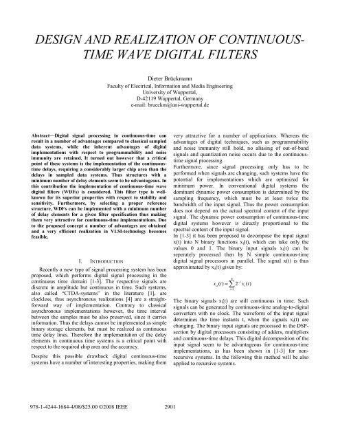
DESIGN AND REALIZATION OF CONTINUOUS-<br />
TIME WAVE DIGITAL FILTERS<br />
Dieter Brückmann<br />
Faculty <strong>of</strong> Electrical, Information <strong>and</strong> Media Engineering<br />
University <strong>of</strong> Wuppertal,<br />
D-42119 Wuppertal, Germany<br />
e-mail: brueckm@uni-wuppertal.de<br />
Abstract—<strong>Digital</strong> signal processing in continuous-time can<br />
result in a number <strong>of</strong> advantages compared to classical sampled<br />
data systems, while the inherent advantages <strong>of</strong> digital<br />
implementations with respect to programmability <strong>and</strong> noise<br />
immunity are retained. It turned out however that a critical<br />
point <strong>of</strong> these systems is the implementation <strong>of</strong> the continuoustime<br />
delays, requiring a considerably larger chip area than the<br />
delays in sampled data systems. Thus structures with a<br />
minimum number <strong>of</strong> delay elements seem to be advantageous. In<br />
this contribution the implementation <strong>of</strong> continuous-time wave<br />
digital filters (WDFs) is considered. This filter type is wellknown<br />
for its superior properties with respect to stability <strong>and</strong><br />
sensitivity. Furthermore, by selecting a proper reference<br />
structure, WDFs can be implemented with a minimum number<br />
<strong>of</strong> delay elements for a given filter specification thus making<br />
them very attractive for continuous-time implementations. Due<br />
to the proposed concept a number <strong>of</strong> advantages are obtained<br />
<strong>and</strong> a very efficient realization in VLSI-technology becomes<br />
feasible.<br />
I. INTRODUCTION<br />
Recently a new type <strong>of</strong> signal processing system has been<br />
proposed, which performs digital signal processing in the<br />
continuous time domain [1-3]. The respective signals are<br />
discrete in amplitude but continuous in time. Such systems,<br />
also called “CTDA-systems” in the literature [1], are<br />
clockless, thus asynchronous realizations [4] are a straightforward<br />
way <strong>of</strong> implementation. Contrary to classical<br />
asynchronous implementations however, the time interval<br />
between the samples must be also preserved, since it carries<br />
information. Thus the delays cannot be implemented as simple<br />
binary storage elements, but must be realized as continuous<br />
time delay lines. Therefore the implementation <strong>of</strong> the delay<br />
elements in continuous time systems is a critical point with<br />
respect to the required chip area <strong>and</strong> the accuracy.<br />
Despite this possible drawback digital continuous-time<br />
systems have a number <strong>of</strong> interesting properties, making them<br />
very attractive for a number <strong>of</strong> applications. Whereas the<br />
advantages <strong>of</strong> digital techniques, such as programmability<br />
<strong>and</strong> noise immunity still hold, no aliasing <strong>of</strong> out-<strong>of</strong>-b<strong>and</strong><br />
signals <strong>and</strong> quantization noise occurs due to the continuoustime<br />
signal processing.<br />
Furthermore, since signal processing only has to be<br />
performed when signals are changing, such systems have the<br />
potential for implementations which are optimized for<br />
minimum power. In conventional digital systems the<br />
dominant dynamic power consumption is determined by the<br />
sampling frequency, which must be at least twice the<br />
b<strong>and</strong>width <strong>of</strong> the input signal. Thus the power consumption<br />
does not depend on the actual spectral content <strong>of</strong> the input<br />
signal. The dynamic power consumption <strong>of</strong> continuous-time<br />
digital systems however is directly proportional to the<br />
spectral content <strong>of</strong> the input signal.<br />
In [1-3] it has been proposed to decompose the input signal<br />
x(t) into N binary functions x i (t), which can take only the<br />
values 0 <strong>and</strong> 1. The binary input signals x i (t) can be<br />
seperately processed then by N simple continuous-time<br />
digital signal processors in parallel. The signal x(t) is thus<br />
approximated by x a (t) given by:<br />
x ( t)<br />
=<br />
a<br />
N<br />
<br />
i=<br />
1<br />
2<br />
x ( t)<br />
−i<br />
i<br />
The binary signals x i (t) are still continuous in time. Such<br />
signals can be generated by continuous-time analog-to-digital<br />
converters with no clock. The waveform <strong>of</strong> the input signal<br />
determines the time instants t i when the signals x i (t) are<br />
changing. The binary input signals are processed in the DSPsection<br />
by digital processors consisting <strong>of</strong> adders, multipliers<br />
<strong>and</strong> continuous-time delays. This digital decomposition <strong>of</strong> the<br />
input signal seem to be advantageous for continuous-time<br />
implementations, as has been shown in [1-3] for nonrecursive<br />
systems. In the following this method will be also<br />
applied to recursive systems.<br />
978-1-4244-1684-4/08/$25.00 ©2008 IEEE 2901
II.<br />
CONTINUOUS-TIME RECURSIVE DIGITAL FILTERS<br />
The transfer function <strong>of</strong> a recursive filter <strong>of</strong> order n can be<br />
described by an n th -order denominator polynomial <strong>and</strong> a<br />
numerator polynomial <strong>of</strong> order m≤n. In order to reduce the<br />
sensitivity with respect to coefficient quantization, the transfer<br />
function is factorized in second-order product terms <strong>and</strong> one<br />
first order term for odd order filters. Such a system can be<br />
implemented by a cascade connection <strong>of</strong> second-order blocks,<br />
<strong>and</strong> one first order block for odd-order filters. The transfer<br />
function H(s) <strong>of</strong> a continuous-time second order digital filter<br />
block is given in the frequency domain s by:<br />
B + B e + B e<br />
= , (2)<br />
−sT<br />
−2sT<br />
0 1<br />
2<br />
H( s)<br />
−sT<br />
−2sT<br />
1+<br />
A1<br />
e + A2e<br />
where T is the fixed delay <strong>of</strong> one delay element D <strong>and</strong> the<br />
B i ’s <strong>and</strong> A i ’s are the filter coefficients. The frequency<br />
response is periodic with frequency 2π/T even though no<br />
aliasing occurs.<br />
The Laplace transform Y(s) <strong>of</strong> the output signal y(t) <strong>of</strong> the<br />
filter block is obtained from the Laplace transform X a (s) <strong>of</strong><br />
the input x a (t) according to<br />
Y( s)<br />
= H(<br />
s)<br />
⋅ X ( s)<br />
. (3)<br />
Using binary decomposition <strong>of</strong> x a (t) each binary bit-stream<br />
must be filtered by the transfer function according to eq. (2).<br />
Figure 1 shows the respective realization. Each <strong>of</strong> the N<br />
parallel filter blocks contains two binary delay elements.<br />
Since the inputs to the multipliers are binary, the multipliers<br />
are degenerated to simple gating functions thus considerably<br />
simplifying the implementation. For an input signal <strong>of</strong> 1 the<br />
coefficient value is gated to the adders <strong>and</strong> for a zero no<br />
gating is performed. Thus the overall realization is<br />
significantly simplified by using N parallel filter block with<br />
the word-length <strong>of</strong> 1 Bit. The output signal y(t) is generated<br />
by a continuous-time adder array taking the binary weighting<br />
x(t)<br />
x(t) 3<br />
x(t) 1<br />
x(t) 2<br />
continuous-time<br />
digital adder<br />
a<br />
B 0<br />
D<br />
-A 1<br />
B 1<br />
D<br />
-A 2<br />
B 2<br />
continuous-time<br />
weighted digital adder<br />
continuous-time<br />
delay, 1 Bit<br />
Figure 1. Decomposition <strong>of</strong> a recursive continuous-time digital filter<br />
block <strong>of</strong> order 2.<br />
y(t)<br />
<strong>of</strong> the respective filter block outputs into account. A second<br />
adder array is required at the input <strong>of</strong> the filter blocks<br />
realizing the recursive functionality.<br />
III.<br />
CONTINUOUS-TIME WAVE DIGITAL FILTERS<br />
Recursive filters based on wave digital filters [5-7] have a<br />
number <strong>of</strong> advantages compared to the structure considered up<br />
to now. Especially they have superior stability properties even<br />
under nonlinear operating conditions caused by rounding or<br />
overflow. Furthermore for a fixed word-length they have a<br />
better dynamic range than filters with cascaded general second<br />
order blocks. <strong>Wave</strong> digital filters are derived from a passive<br />
reference prototype <strong>and</strong> the superior properties <strong>of</strong> the analog<br />
reference structure are mapped to the digital filter when<br />
properly designed. For the realization <strong>of</strong> wave digital filters<br />
there exists a number <strong>of</strong> different structures. It turned out that<br />
wave digital filters in lattice structure [5-7], result in<br />
implementations with minimum hardware requirements. The<br />
coefficients <strong>of</strong> these filters can be easily obtained from explicit<br />
formulas as described in [6]. Respective s<strong>of</strong>tware tools are<br />
available for the coefficient computation.<br />
Lattice wave digital filters are composed <strong>of</strong> two branches<br />
which consist <strong>of</strong> cascaded second order allpass sections <strong>and</strong><br />
one first order allpass in the upper branch as shown in fig. 2.<br />
Since the number <strong>of</strong> delay elements is canonical, these<br />
structures seem to be well-suited for continuous-time<br />
implementations.<br />
x(t)<br />
γ 2m+1<br />
γ 2<br />
D<br />
D<br />
γ 0<br />
γ 2m+3<br />
D<br />
D<br />
γ 2m+2<br />
γ 2m+4<br />
γ 1<br />
D<br />
γ 2m<br />
γ 2m-1<br />
γ 2(m+n)-1<br />
γ 2(m+n)<br />
D D D<br />
D<br />
D<br />
D<br />
+<br />
-<br />
Figure 2. <strong>Continuous</strong>-time <strong>Wave</strong> <strong>Digital</strong> Filter in lattice<br />
structure.<br />
1<br />
2<br />
y(t)<br />
2902
The transfer function H(s) <strong>of</strong> this continuous-time wave<br />
digital filter can be described by the transfer functions H 1 (s)<br />
<strong>and</strong> H 2 (s) <strong>of</strong> the two allpass branches:<br />
H1(<br />
s)<br />
− H<br />
2<br />
( s)<br />
H( s)<br />
= (4)<br />
2<br />
For the transfer function A 1 (s) <strong>of</strong> the continuous-time first<br />
order allpass section holds:<br />
− γ<br />
0<br />
+ e<br />
A1<br />
( s)<br />
=<br />
1−γ<br />
⋅ e<br />
0<br />
−sT<br />
−sT<br />
where the coefficient γ 0 is in the range –1
In [1] <strong>and</strong> [2] an architecture with an ADC using delta<br />
modulation was proposed, so that the input signal to the FIR-<br />
Filter is represented by a 1-Bit stream. Thus 1-Bit delay<br />
elements for each tap are sufficient <strong>and</strong> a 1-Bit signal<br />
representation can be used for most <strong>of</strong> the datapath.<br />
Thus the required chip area can be reduced for the FIR-<br />
Filter. Due to the recursive structure this does not hold<br />
however for the delay elements <strong>of</strong> the WDFs, if the<br />
wordlength <strong>of</strong> the input signal is 1 Bit.<br />
Figure 4. Frequency characteristics <strong>of</strong> the continuous-time<br />
filters with optimized coefficient values <strong>and</strong> minimum internal<br />
wordlength.<br />
In order to compare the different realizations with respect<br />
to implementation costs following cost function was defined:<br />
CO =<br />
N<br />
<br />
n=<br />
1<br />
m<br />
0, n<br />
+<br />
( L−1)<br />
/ 2 N<br />
<br />
i= 1 n=<br />
1<br />
m<br />
i,<br />
n<br />
+ F ⋅<br />
L<br />
N<br />
<br />
i= 1 n=<br />
1<br />
d<br />
i,<br />
n<br />
, (8)<br />
where N is the required wordlength <strong>and</strong> corresponds to the<br />
number <strong>of</strong> parallel processing blocks in fig. 1. L is the filter<br />
order, m i,n is the number <strong>of</strong> 1-Bit adders in section i, <strong>and</strong> d i,n<br />
is the number <strong>of</strong> 1-Bit delay elements in the respective<br />
section. The number <strong>of</strong> adders in each first order section is<br />
given by m 0,n . The form factor F is determined by the ratio <strong>of</strong><br />
the chip area required for a 1-Bit delay element to the chip<br />
area for a 1-Bit adder.<br />
Taking the coefficient representation according to table I<br />
into account, 574 adders (1-Bit) <strong>and</strong> 98 delay elements (1- Bit)<br />
are required for the 7 th -order lattice filter. The 10 th -order<br />
bireciprocal filter can be realized with 194 adders <strong>and</strong> 120<br />
delay elements. Thus, using eq. 8, it turns out that for form<br />
factors F greater than 17 the 7 th -order filter is the better<br />
solution with respect to implementation costs, otherwise the<br />
bireciprocal filter is the WDF-architecture to be preferred.<br />
A direct implementation <strong>of</strong> the FIR-filter requires<br />
28x12=336 delay elements <strong>and</strong> more than 300 adders, which<br />
results in drastically increased implementation costs compared<br />
to the recursive filter structures.<br />
The granularity required for the continuous-time delay<br />
elements is determined by the highest rate <strong>of</strong> change <strong>of</strong> the<br />
input signal. This granularity is directly related to the chip area<br />
required for implementation.<br />
V. CONCLUSIONS<br />
<strong>Continuous</strong>-time digital filters, recently proposed, can<br />
have some advantages compared to conventional sampled data<br />
systems. Due to the nonsampled operation no aliasing <strong>of</strong><br />
higher frequency components <strong>and</strong> <strong>of</strong> noise occurs <strong>and</strong> due to<br />
the asynchronous operation the power consumption can be<br />
minimized.<br />
In this contribution it had been shown how to implement<br />
recursive continuous-time filters. In order to compare the<br />
implementation costs <strong>of</strong> different filter architectures a cost<br />
function had been defined. Using this cost function two<br />
different structures <strong>of</strong> wave digital filters had been compared<br />
to each other <strong>and</strong> to a continuous-time FIR-filter. It turned out<br />
that it can be advantageous with respect to implementation<br />
costs to use the recursive filter structures. It has been shown<br />
that the required chip area can be considerably reduced if the<br />
filter is properly designed.<br />
REFERENCES<br />
[1] Y. P. Tsividis, “Mixed-Domain Systems <strong>and</strong> Signal Processing Based<br />
on Input Decomposition”, IEEE Transactions on Circuits <strong>and</strong> Systems<br />
– I: Regular Papers, vol. 53, no. 10, pp. 2145-2156, 2006.<br />
[2] Y. W. Lee, K. L. Shepard, Y. P. Tsividis, “A <strong>Continuous</strong>-<strong>Time</strong><br />
Programmable <strong>Digital</strong> FIR-Filter”, IEEE Journal <strong>of</strong> Solid State<br />
Circuits, vol. 39, no. 21, pp. 2512-2520, 2006.<br />
[3] Y. P. Tsividis, “<strong>Continuous</strong>-<strong>Time</strong> digital signal processing”, Electronic<br />
letters, vol. 41, no. 11, pp. 1551-1552, 2003.<br />
[4] F. Aeschlimann, E. Allier, L. Fesquet, <strong>and</strong> M. Renaudin,<br />
“Asynchronous FIR-<strong>Filters</strong>: towards a new digital processing chain”,<br />
Proc. Int. Symp. Asynchronous Circ. Syst., pp. 198-206, 2004.<br />
[5] A. Fettweis, "<strong>Wave</strong> digital filters: Theory <strong>and</strong> practice", Proc. IEEE,<br />
vol. 74, p. 270-327, Feb. 1986.<br />
[6] L. Gazsi, "Explicit formulas for lattice wave digital filters", IEEE<br />
Trans. Circuits Systems, vol. 32, no. 2, p. 68-88, 1985.<br />
[7] D. Brückmann, "Optimised <strong>Digital</strong> Signal Processing for Flexible<br />
Receivers", Proc. ICASSP 2002, Orl<strong>and</strong>o, Fl., USA, 13.-17. Mai 2002.<br />
[8] D. Brückmann, L. Bouhrize, “Filter stages for a high-performance<br />
reconfigurable radio receiver with minimum system delay”,<br />
Proceedings ICASSP 2007, Honolulu, Hawaii, USA, 15.-20. April<br />
2007.<br />
[9] J. Y. Kaakinen <strong>and</strong> T. Saramäki, “<strong>Design</strong> <strong>of</strong> Very Low-Sensitivity <strong>and</strong><br />
Low-Noise Recursive <strong>Filters</strong> Using a Cascade <strong>of</strong> Low-Order Lattice<br />
wave <strong>Digital</strong> <strong>Filters</strong>”, IEEE Transactions on Circuits <strong>and</strong> Systems – II:<br />
Analog <strong>and</strong> <strong>Digital</strong> Signal Processing, vol. 46, no. 7, pp. 906-914,1999.<br />
2904