MC3335 Low Power Narrowband FM Receiver
MC3335 Low Power Narrowband FM Receiver
MC3335 Low Power Narrowband FM Receiver

Create successful ePaper yourself
Turn your PDF publications into a flip-book with our unique Google optimized e-Paper software.
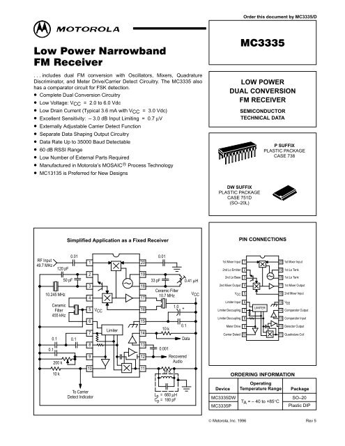
Order this document by <strong>MC3335</strong>/D<br />
<br />
<br />
. . . includes dual <strong>FM</strong> conversion with Oscillators, Mixers, Quadrature<br />
Discriminator, and Meter Drive/Carrier Detect Circuitry. The <strong>MC3335</strong> also<br />
has a comparator circuit for FSK detection.<br />
• Complete Dual Conversion Circuitry<br />
• <strong>Low</strong> Voltage: VCC = 2.0 to 6.0 Vdc<br />
• <strong>Low</strong> Drain Current (Typical 3.6 mA with VCC = 3.0 Vdc)<br />
• Excellent Sensitivity: – 3.0 dB Input Limiting = 0.7 µV<br />
• Externally Adjustable Carrier Detect Function<br />
• Separate Data Shaping Output Circuitry<br />
• Data Rate Up to 35000 Baud Detectable<br />
• 60 dB RSSI Range<br />
• <strong>Low</strong> Number of External Parts Required<br />
• Manufactured in Motorola′s MOSAIC® Process Technology<br />
• MC13135 is Preferred for New Designs<br />
<br />
LOW POWER<br />
DUAL CONVERSION<br />
<strong>FM</strong> RECEIVER<br />
SEMICONDUCTOR<br />
TECHNICAL DATA<br />
P SUFFIX<br />
PLASTIC PACKAGE<br />
CASE 738<br />
DW SUFFIX<br />
PLASTIC PACKAGE<br />
CASE 751D<br />
(SO–20L)<br />
Simplified Application as a Fixed <strong>Receiver</strong><br />
PIN CONNECTIONS<br />
RF Input<br />
49.7 MHz<br />
120 pF<br />
10.245 MHz<br />
Ceramic<br />
Filter<br />
455 kHz<br />
0.1<br />
0.1 0.1<br />
200 k<br />
10 k<br />
50 pF<br />
0.01<br />
1<br />
2<br />
3<br />
4<br />
5<br />
6<br />
7<br />
8<br />
9<br />
10<br />
VCC<br />
Limiter<br />
20<br />
19<br />
18<br />
17<br />
16<br />
15<br />
14<br />
13<br />
12<br />
11<br />
33 pF<br />
0.01<br />
Ceramic Filter<br />
10.7 MHz<br />
10 k<br />
39 K<br />
1.0<br />
+<br />
0.1<br />
0.001<br />
Recovered<br />
Audio<br />
0.41 µH<br />
Data<br />
VCC<br />
1st Mixer Input<br />
1<br />
2nd Lo Emitter 2<br />
2nd Lo Base 3<br />
2nd Mixer Output<br />
4<br />
8<br />
9<br />
Carrier Detect 10<br />
20 1st Mixer Input<br />
19 1st Lo Tank<br />
18 1st Lo Tank<br />
17 1st Mixer Output<br />
V CC 5<br />
16 2nd Mixer Input<br />
Limiter Input 6 15 V EE<br />
Limiter Decoupling 7<br />
LIMITER<br />
14 Comparator Output<br />
Limiter Decoupling<br />
Meter Drive<br />
13 Comparator Input<br />
12 Detector Output<br />
ORDERING INFORMATION<br />
11<br />
Quadrature Coil<br />
To Carrier<br />
Detect Indicator<br />
Lp = 660 µH<br />
Cp = 180 pF<br />
Device<br />
<strong>MC3335</strong>DW<br />
<strong>MC3335</strong>P<br />
Operating<br />
Temperature Range<br />
TA = – 40 to +85°C<br />
Package<br />
SO–20<br />
Plastic DIP<br />
MOTOROLA ANALOG IC DEVICE DATA<br />
© Motorola, Inc. 1996 Rev 5<br />
1
<strong>MC3335</strong><br />
MAXIMUM RATINGS (TA = 25°C, unless otherwise noted)<br />
Rating Pin Symbol Value Unit<br />
<strong>Power</strong> Supply Voltage 5 VCC(max) 7.0 Vdc<br />
Operating Supply Voltage Range<br />
(Recommended)<br />
5 VCC 2.0 to 6.0 Vdc<br />
Input Voltage (VCC > 5.0 Vdc) 1,20 V1–20 1.0 Vrms<br />
Junction Temperature – TJ 150 °C<br />
Operating Ambient Temperature Range – TA – 40 to + 85 °C<br />
Storage Temperature Range – Tstg – 65 to + 150 °C<br />
ELECTRICAL CHARACTERISTICS (VCC = 5.0 Vdc, fo = 49.7 MHz, Deviation = 3.0 kHz, TA = 25°C, test circuit of Figure 2,<br />
unless otherwise noted.)<br />
Characteristic Pin Min Typ Max Unit<br />
Drain Current 5 – 4.5 7.0 mAdc<br />
Input for – 3.0 dB Limiting – – 0.7 2.0 µVrms<br />
Recovered Audio (RF Signal Level = 1.0 mV) 12 – 250 – mVrms<br />
Noise Output (RF Signal Level = 0 mV) 12 – 250 – mVrms<br />
Carrier Detect Threshold (below VCC) 9 – 0.64 – Vdc<br />
Meter Drive Slope 9 – 100 – µA/dB<br />
Input for 20 dB (S +N/N) – – 1.3 – µVrms<br />
First Mixer 3rd Order Intercept (Input) – – – 20 – dBm<br />
First Mixer Input Resistance (Rp) – – 690 – Ω<br />
First Mixer Input Capacitance (Cp) – – 7.2 – pF<br />
First Mixer Conversion Voltage Gain – – 18 – dB<br />
Second Mixer Conversion Voltage Gain – – 21 – dB<br />
Detector Output Resistance 12 – 1.4 – kΩ<br />
RF Input<br />
49.7 MHz<br />
0.1<br />
2.6<br />
Figure 1. Test Circuit<br />
VCC<br />
56 pF<br />
10.245 MHz<br />
39 pF<br />
Ceramic<br />
Filter<br />
455 kHz<br />
1<br />
2<br />
3<br />
4<br />
5<br />
VCC<br />
20<br />
19<br />
18<br />
17<br />
16<br />
20 k<br />
1.4<br />
39 MHz<br />
Ceramic Filter<br />
10.7 MHz<br />
1.0<br />
+<br />
300<br />
0.1<br />
0.1 0.1<br />
6<br />
7<br />
8<br />
15<br />
14<br />
13<br />
0.01<br />
0.1<br />
200 k<br />
10 k<br />
9<br />
10<br />
12<br />
11<br />
7.5 k<br />
68 k<br />
RA<br />
To Carrier<br />
Detect Indicator<br />
Lp = 660 µH<br />
Cp = 180 pF<br />
2 MOTOROLA ANALOG IC DEVICE DATA
<strong>MC3335</strong><br />
I 9 ( µ A)<br />
Figure 2. Imeter versus Input<br />
12<br />
11 VCC<br />
10 A<br />
9<br />
<strong>MC3335</strong><br />
9.0<br />
8.0<br />
7.0<br />
6.0<br />
5.0<br />
4.0<br />
3.0<br />
2.0<br />
– 130<br />
– 120 – 110 – 100 –90 –80 – 70 –60 –50<br />
RF INPUT (dBm)<br />
–40<br />
–30<br />
I<br />
CC<br />
(mA)<br />
8.0<br />
7.0<br />
6.0<br />
5.0<br />
4.0<br />
3.0<br />
2.0<br />
1.0<br />
0<br />
0<br />
1.0<br />
Figure 3. Drain Current, Recovered<br />
Audio versus Supply<br />
2.0<br />
ICC, Carr. Det. <strong>Low</strong> (RF in = 10 mV)<br />
ICC, Carr. Det. High (RF in = 0 mV)<br />
3.0<br />
4.0<br />
VCC (V)<br />
Recovered Audio<br />
800<br />
700<br />
600<br />
500<br />
400<br />
300<br />
200<br />
100<br />
0<br />
5.0 6.0 7.0 8.0<br />
V 12 (mVrms)<br />
(S + N)/N (dB)<br />
20<br />
10<br />
0<br />
–10<br />
–20<br />
–30<br />
–40<br />
–50<br />
–60<br />
–70<br />
–80<br />
– 130<br />
Figure 4. (S + N), N of 2nd Mixer<br />
S+N<br />
N<br />
– 120 – 110 – 100 –90 –80 – 70 –60 –50<br />
RF INPUT (dBm)<br />
–40<br />
–30<br />
(S + N)/N (dB)<br />
20<br />
10<br />
0<br />
–10<br />
–20<br />
–30<br />
–40<br />
–50<br />
–60<br />
–70<br />
–80<br />
– 130<br />
Figure 5. (S + N)/N versus Input<br />
12 7.5 k<br />
<strong>MC3335</strong><br />
0.01<br />
– 120 – 110 – 100 –90 –80 – 70<br />
RF INPUT (dBm)<br />
S+N<br />
N<br />
–60 –50<br />
–40<br />
–30<br />
(dB)<br />
20<br />
10<br />
0<br />
–10<br />
–20<br />
–30<br />
–40<br />
–50<br />
–60<br />
–70<br />
Figure 6. 1st Mixer 3rd Order Intermodulation<br />
Desired Products<br />
–80<br />
– 100 –90 –80 – 70<br />
–60 –50 –40<br />
RF INPUT (dBm)<br />
3rd Order Intermod.<br />
Products<br />
–30<br />
–20 –10<br />
0<br />
V 12 (Vdc)<br />
Figure 7. Detector Output versus Frequency<br />
4.0<br />
3.0<br />
2.0<br />
1.0<br />
0<br />
–40 –30 –20 –10 0 10 20 30 40<br />
RELATIVE INPUT FREQUENCY (kHz)<br />
MOTOROLA ANALOG IC DEVICE DATA<br />
3
CIRCUIT DESCRIPTION<br />
<strong>MC3335</strong><br />
The <strong>MC3335</strong> is a complete <strong>FM</strong> narrowband receiver from<br />
antenna input to audio preamp output. The low voltage dual<br />
conversion design yields low power drain, excellent<br />
sensitivity and good image rejection in narrowband voice and<br />
data link applications.<br />
In the typical application diagram, the first mixer amplifies<br />
the signal and converts the RF input to 10.7 MHz. This IF<br />
signal is filtered externally and fed into the second mixer,<br />
which further amplifies the signal and converts it to a 455 kHz<br />
IF signal. After external bandpass filtering, the low IF is fed<br />
into the limiting amplifier and detection circuitry. The audio is<br />
recovered using a conventional quadrature detector.<br />
Twice–IF filtering is provided internally.<br />
The input signal level is monitored by meter drive circuitry<br />
which detects the amount of limiting in the limiting amplifier.<br />
The voltage at the meter drive pin determines the state of the<br />
carrier detect output which is active low.<br />
APPLICATIONS INFORMATION<br />
The first local oscillator can be run using a free running LC<br />
tank, as a VCO using PLL synthesis, or driven from an<br />
external crystal oscillator. At higher VCC values (6.0 to<br />
7.0 V), it has been run to 170 MHz. The second local<br />
oscillator is a common base Colpitts type which is typically<br />
run at 10.245 MHz under crystal control.<br />
The mixers are doubly balanced to reduce spurious<br />
responses. The first and second mixers have conversion<br />
gains of 18 dB and 22 dB (typical), respectively. Mixer gain is<br />
stable with respect to supply voltage. For both conversions,<br />
the mixer impedances and pin layout are designed to allow<br />
the user to employ low cost, readily available ceramic filters.<br />
Overall sensitivity is shown in Figure 5. The input level for<br />
20 dB (S + N)/N is 1.3 µV using the two–pole post–detection<br />
filter as demonstrated.<br />
Following the first mixer, a 10.7 MHz ceramic bandpass<br />
filter is recommended. The 10.7 MHz filtered signal is then<br />
fed into one second mixer input pin, the other input pin being<br />
connected to VCC. Pin 5 (VCC) is treated as a common point<br />
for emitter–driven signals.<br />
The 455 kHz IF is typically filtered using a ceramic<br />
bandpass filter, then fed into the limiter input pin. The limiter<br />
has 10 µV sensitivity for –3.0 dB limiting, flat to 1.0 MHz.<br />
The output of the limiter is internally connected to the<br />
quadrature detector, including a quadrature capacitor. A<br />
parallel LC tank is needed externally from Pin 11 to VCC.<br />
A 39 kΩ shunt resistance is included which determines the<br />
peak separation of the quadrature detector; a smaller value<br />
will increase the spacing and linearity but decrease<br />
recovered audio and sensitivity.<br />
A data shaping circuit is available and can be coupled to<br />
the recovered audio output of Pin 12. The circuit is a<br />
comparator which is designed to detect zero crossings of<br />
FSK modulation. Data rates of up to 35000 baud are<br />
detectable using the typical application. Hysteresis is<br />
available by connecting a high–valued resistor from Pin 13 to<br />
Pin 14. Values below 120 kΩ are not recommended as the<br />
input signal cannot overcome the hysteresis.<br />
The meter drive circuitry detects input signal level by<br />
monitoring the limiting of the limiting amplifier stages.<br />
Figure 2 shows the unloaded current at Pin 9 versus input<br />
power. The meter drive current can be used directly (RSSI)<br />
or can be used to trip the carrier detect circuit at a specified<br />
input power. To do this, pick an RF trip level in dBm. Read the<br />
corresponding current from Figure 2 and pick a resistor such<br />
that:<br />
R9 = 0.64 Vdc / I9<br />
Hysteresis is available by connecting a high–valued<br />
resistor RH between Pin 9 and 10. The formula is:<br />
Hysteresis = VCC/(RH x 10–7) dB<br />
4 MOTOROLA ANALOG IC DEVICE DATA
<strong>MC3335</strong><br />
OUTLINE DIMENSIONS<br />
–A<br />
–<br />
20<br />
11<br />
B<br />
1 10<br />
C<br />
P SUFFIX<br />
PLASTIC PACKAGE<br />
CASE 738–03<br />
L<br />
NOTES:<br />
1. DIMENSIONING AND TOLERANCING PER ANSI<br />
Y14.5M, 1982.<br />
2. CONTROLLING DIMENSION: INCH.<br />
3. DIMENSION “L” TO CENTER OF LEAD WHEN<br />
FORMED PARALLEL.<br />
4. DIMENSION “B” DOES NOT INCLUDE MOLD<br />
FLASH.<br />
5. 738–02 OBSOLETE, NEW STANDARD 738–03.<br />
–T<br />
SEATING –<br />
PLANE<br />
G<br />
E<br />
F<br />
D 20 PL<br />
N<br />
K<br />
0.25 (0.010) M T A<br />
M<br />
J 20 PL<br />
M<br />
0.25 (0.010) M T B<br />
M<br />
DIM<br />
A<br />
B<br />
C<br />
D<br />
E<br />
F<br />
G<br />
J<br />
K<br />
L<br />
M<br />
N<br />
MILLIMETERS<br />
MIN MAX<br />
25.66 27.17<br />
6.10 6.60<br />
3.81 4.57<br />
0.39 0.55<br />
1.27 BSC<br />
1.27 1.77<br />
2.54 BSC<br />
0.21 0.38<br />
2.80 3.55<br />
7.62 BSC<br />
0°<br />
0.51<br />
15°<br />
1.01<br />
INCHES<br />
MIN MAX<br />
1.010 1.070<br />
0.240 0.260<br />
0.150 0.180<br />
0.015 0.022<br />
0.050 BSC<br />
0.050 0.070<br />
0.100 BSC<br />
0.008 0.015<br />
0.110 0.140<br />
0.300 BSC<br />
0°<br />
0.020<br />
15°<br />
0.040<br />
20<br />
–A<br />
–<br />
11<br />
–B P<br />
–<br />
1 10<br />
10 PL<br />
DW SUFFIX<br />
PLASTIC PACKAGE<br />
CASE 751D–03<br />
(SO–20L)<br />
0.25 (0.010) M B<br />
M<br />
NOTES:<br />
1. DIMENSIONING AND TOLERANCING PER ANSI<br />
Y14.5M, 1982.<br />
2. CONTROLLING DIMENSION: MILLIMETER.<br />
3. DIMENSION A AND B DO NOT INCLUDE MOLD<br />
PROTRUSION.<br />
4. MAXIMUM MOLD PROTRUSION 0.15 (0.006) PER<br />
SIDE.<br />
5. 751D–01, AND –02 OBSOLETE, NEW STANDARD<br />
751D–03.<br />
G<br />
–T<br />
SEATING –<br />
PLANE<br />
D 20 PL<br />
C<br />
K<br />
0.25 (0.010) M T B S A S<br />
M<br />
F<br />
R X 45°<br />
J<br />
DIM<br />
A<br />
B<br />
C<br />
D<br />
F<br />
G<br />
J<br />
K<br />
M<br />
P<br />
R<br />
MILLIMETERS<br />
MIN MAX<br />
12.65 12.95<br />
7.40 7.60<br />
2.35 2.65<br />
0.35 0.49<br />
0.50 0.90<br />
INCHES<br />
MIN MAX<br />
0.499 0.510<br />
0.292 0.299<br />
0.093 0.104<br />
0.014 0.019<br />
0.020 0.035<br />
1.27 BSC 0.050 BSC<br />
0.32 0.010<br />
0.25 0.004<br />
7° 0°<br />
10.55 0.395<br />
0.75 0.010<br />
0.25<br />
0.10<br />
0°<br />
10.05<br />
0.25<br />
0.012<br />
0.009<br />
7°<br />
0.415<br />
0.029<br />
MOTOROLA ANALOG IC DEVICE DATA<br />
5
<strong>MC3335</strong><br />
Motorola reserves the right to make changes without further notice to any products herein. Motorola makes no warranty, representation or guarantee regarding<br />
the suitability of its products for any particular purpose, nor does Motorola assume any liability arising out of the application or use of any product or circuit, and<br />
specifically disclaims any and all liability, including without limitation consequential or incidental damages. “Typical” parameters which may be provided in Motorola<br />
data sheets and/or specifications can and do vary in different applications and actual performance may vary over time. All operating parameters, including “Typicals”<br />
must be validated for each customer application by customer’s technical experts. Motorola does not convey any license under its patent rights nor the rights of<br />
others. Motorola products are not designed, intended, or authorized for use as components in systems intended for surgical implant into the body, or other<br />
applications intended to support or sustain life, or for any other application in which the failure of the Motorola product could create a situation where personal injury<br />
or death may occur. Should Buyer purchase or use Motorola products for any such unintended or unauthorized application, Buyer shall indemnify and hold Motorola<br />
and its officers, employees, subsidiaries, affiliates, and distributors harmless against all claims, costs, damages, and expenses, and reasonable attorney fees<br />
arising out of, directly or indirectly, any claim of personal injury or death associated with such unintended or unauthorized use, even if such claim alleges that<br />
Motorola was negligent regarding the design or manufacture of the part. Motorola and are registered trademarks of Motorola, Inc. Motorola, Inc. is an Equal<br />
Opportunity/Affirmative Action Employer.<br />
How to reach us:<br />
USA / EUROPE / Locations Not Listed: Motorola Literature Distribution;<br />
JAPAN: Nippon Motorola Ltd.; Tatsumi–SPD–JLDC, 6F Seibu–Butsuryu–Center,<br />
P.O. Box 20912; Phoenix, Arizona 85036. 1–800–441–2447 or 602–303–5454 3–14–2 Tatsumi Koto–Ku, Tokyo 135, Japan. 03–81–3521–8315<br />
MFAX: RMFAX0@email.sps.mot.com – TOUCHTONE 602–244–6609<br />
ASIA/PACIFIC: Motorola Semiconductors H.K. Ltd.; 8B Tai Ping Industrial Park,<br />
INTERNET: http://Design–NET.com 51 Ting Kok Road, Tai Po, N.T., Hong Kong. 852–26629298<br />
6 ◊<br />
MOTOROLA ANALOG IC DEVICE <strong>MC3335</strong>/D DATA
![AT89C1051 [ä¸ææ°æ®æå] [PDF] - ä¸æºåçæº](https://img.yumpu.com/44984295/1/184x260/at89c1051-a-aeaeaeraea-pdf-a-aeacae.jpg?quality=85)