VIV Low V IXGH 25 N120 1200 V 50 A 3 V High speed IGBT IXGH ...
VIV Low V IXGH 25 N120 1200 V 50 A 3 V High speed IGBT IXGH ...
VIV Low V IXGH 25 N120 1200 V 50 A 3 V High speed IGBT IXGH ...

Create successful ePaper yourself
Turn your PDF publications into a flip-book with our unique Google optimized e-Paper software.
V CES<br />
I C<strong>25</strong><br />
V CE(sat)<br />
<strong>Low</strong> V CE(sat)<br />
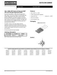
<strong>IXGH</strong> <strong>25</strong> <strong>N120</strong> <strong>1200</strong> V <strong>50</strong> A 3 V<br />
<strong>High</strong> <strong>speed</strong> <strong>IGBT</strong> <strong>IXGH</strong> <strong>25</strong> <strong>N120</strong>A <strong>1200</strong> V <strong>50</strong> A 4 V<br />
Symbol Test Conditions Maximum Ratings<br />
V CES<br />
T J<br />
= <strong>25</strong>°C to 1<strong>50</strong>°C <strong>1200</strong> V<br />
V CGR<br />
T J<br />
= <strong>25</strong>°C to 1<strong>50</strong>°C; R GE<br />
= 1 MΩ <strong>1200</strong> V<br />
V GES<br />
Continuous ±20 V<br />
V GEM<br />
Transient ±30 V<br />
I C<strong>25</strong><br />
T C<br />
= <strong>25</strong>°C <strong>50</strong> A<br />
I C90<br />
T C<br />
= 90°C <strong>25</strong> A<br />
I CM<br />
T C<br />
= <strong>25</strong>°C, 1 ms 100 A<br />
SSOA V GE<br />
= 15 V, T VJ<br />
= 1<strong>25</strong>°C, R G<br />
= 33 Ω I CM<br />
= <strong>50</strong> A<br />
(RBSOA) Clamped inductive load, L = 100 µH @ 0.8 V CES<br />
P C<br />
T C<br />
= <strong>25</strong>°C 200 W<br />
T J<br />
-55 ... +1<strong>50</strong> °C<br />
T JM<br />
1<strong>50</strong> °C<br />
T stg<br />
-55 ... +1<strong>50</strong> °C<br />
M d<br />
Mounting torque (M3) 1.13/10 Nm/lb.in.<br />
Weight 6 g<br />
Maximum lead temperature for soldering 300 °C<br />
1.6 mm (0.062 in.) from case for 10 s<br />
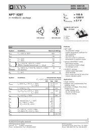
TO-247 AD<br />
G<br />
C<br />
E<br />
G = Gate,<br />
E = Emitter,<br />
C = Collector,<br />
TAB = Collector<br />
Features<br />
l International standard package<br />
JEDEC TO-247 AD<br />
l 2nd generation HDMOS<br />
TM<br />
process<br />
l <strong>Low</strong> VCE(sat)<br />
l<br />
- for low on-state conduction losses<br />
MOS Gate turn-on<br />
- drive simplicity<br />
Symbol Test Conditions Characteristic Values<br />
(T J<br />
= <strong>25</strong>°C, unless otherwise specified)<br />
min. typ. max.<br />
BV CES<br />
I C<br />
= 3 mA, V GE<br />
= 0 V <strong>1200</strong> V<br />
V GE(th)<br />
I C<br />
= <strong>25</strong>0 µA, V CE<br />
= V GE<br />
2.5 6 V<br />
I CES<br />
V CE<br />
= 0.8 • V CES<br />
T J<br />
= <strong>25</strong>°C <strong>25</strong>0 µA<br />
V GE<br />
= 0 V T J<br />
= 1<strong>25</strong>°C 1 mA<br />
I GES<br />
V CE<br />
= 0 V, V GE<br />
= ±20 V ±100 nA<br />
V CE(sat)<br />
I C<br />
= I C90<br />
, V GE<br />
= 15 V <strong>25</strong><strong>N120</strong> 3 V<br />
<strong>25</strong><strong>N120</strong>A 4 V<br />
Applications<br />
l<br />
AC motor <strong>speed</strong> control<br />
l<br />
DC servo and robot drives<br />
l<br />
DC choppers<br />
l<br />
Uninterruptible power supplies (UPS)<br />
l<br />
Switch-mode and resonant-mode<br />
power supplies<br />
l<br />
Capacitor discharge systems<br />
l<br />
Solid state relays<br />
Advantages<br />
l<br />
Easy to mount with 1 screw (TO-247)<br />
(isolated mounting screw hole)<br />
l<br />
<strong>High</strong> power density<br />
© 1996 IXYS All rights reserved<br />
92783D (3/96)
<strong>IXGH</strong> <strong>25</strong><strong>N120</strong><br />
<strong>IXGH</strong> <strong>25</strong><strong>N120</strong>A<br />
Symbol Test Conditions Characteristic Values<br />
(T J<br />
= <strong>25</strong>°C, unless otherwise specified)<br />
min. typ. max.<br />
TO-247 AD Outline<br />
g fs<br />
I C<br />
= I C90<br />
; V CE<br />
= 10 V, 8 15 S<br />
Pulse test, t ≤ 300 µs, duty cycle ≤ 2 %<br />
C ies<br />
27<strong>50</strong> pF<br />
C oes<br />
V CE<br />
= <strong>25</strong> V, V GE<br />
= 0 V, f = 1 MHz 200 pF<br />
C res<br />
<strong>50</strong> pF<br />
Q g<br />
130 180 nC<br />
Q ge<br />
I C<br />
= I C90<br />
, V GE<br />
= 15 V, V CE<br />
= 0.5 V CES<br />
<strong>25</strong> <strong>50</strong> nC<br />
Q gc<br />
55 90 nC<br />
t d(on)<br />
Inductive load, T J<br />
= <strong>25</strong>°C<br />
100 ns<br />
t I<br />
ri C<br />
= I C90<br />
, V GE<br />
= 15 V, L = 100 µH,<br />
<strong>25</strong>0 ns<br />
V<br />
t CE<br />
= 0.8 V CES<br />
, R G<br />
= R off<br />
= 33 Ω<br />
d(off)<br />
6<strong>50</strong> 1000 ns<br />
Remarks: Switching times<br />
t fi<br />
<strong>25</strong><strong>N120</strong> 700 ns<br />
may increase<br />
<strong>25</strong><strong>N120</strong>A 600 800 ns<br />
for V CE<br />
(Clamp) > 0.8 • V CES<br />
,<br />
E off<br />
higher T J<br />
or increased R G<br />
<strong>25</strong><strong>N120</strong>A 11 mJ<br />
1 = Gate<br />
2 = Collector<br />
3 = Emitter<br />
Tab = Collector<br />
t d(on)<br />
100 ns<br />
Inductive load, T<br />
t J<br />
= 1<strong>25</strong>°C<br />
ri<br />
<strong>25</strong>0 ns<br />
I<br />
E C<br />
= I C90<br />
, V GE<br />
= 15 V, L = 100 µH<br />
on<br />
4.2 mJ<br />
V<br />
t CE<br />
= 0.8 V CES<br />
, R G<br />
= R off<br />
= 33 Ω<br />
d(off)<br />
720 1000 ns<br />
Remarks: Switching times<br />
t fi may increase<br />
<strong>25</strong><strong>N120</strong> <strong>1200</strong> ns<br />
<strong>25</strong><strong>N120</strong>A 800 <strong>1200</strong> ns<br />
for V CE<br />
(Clamp) > 0.8 • V CES<br />
,<br />
E off<br />
higher T J<br />
or increased R G<br />
<strong>25</strong><strong>N120</strong>A 15 mJ<br />
R thJC<br />
0.62 K/W<br />
R thCK<br />
0.<strong>25</strong> K/W<br />
IXYS reserves the right to change limits, test conditions, and dimensions.<br />
IXYS MOSFETS and <strong>IGBT</strong>s are covered by one or more of the following U.S. patents: 4,835,592 4,881,106 5,017,<strong>50</strong>8 5,049,961 5,187,117 5,486,715<br />
4,8<strong>50</strong>,072 4,931,844 5,034,796 5,063,307 5,237,481 5,381,0<strong>25</strong>
![AT89C1051 [ä¸ææ°æ®æå] [PDF] - ä¸æºåçæº](https://img.yumpu.com/44984295/1/184x260/at89c1051-a-aeaeaeraea-pdf-a-aeacae.jpg?quality=85)