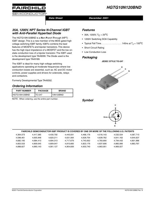
HGTG10N120BND - Fairchild Semiconductor
HGTG10N120BND - Fairchild Semiconductor
HGTG10N120BND - Fairchild Semiconductor

You also want an ePaper? Increase the reach of your titles
YUMPU automatically turns print PDFs into web optimized ePapers that Google loves.
<strong>HGTG10N120BND</strong><br />
Data Sheet December 2001<br />
35A, 1200V, NPT Series N-Channel IGBT<br />
with Anti-Parallel Hyperfast Diode<br />
The <strong>HGTG10N120BND</strong> is a Non-Punch Through (NPT)<br />
IGBT design. This is a new member of the MOS gated high<br />
voltage switching IGBT family. IGBTs combine the best<br />
features of MOSFETs and bipolar transistors. This device<br />
has the high input impedance of a MOSFET and the low onstate<br />
conduction loss of a bipolar transistor. The IGBT used<br />
is the development type TA49290. The Diode used is the<br />
development type TA49189.<br />
The IGBT is ideal for many high voltage switching<br />
applications operating at moderate frequencies where low<br />
conduction losses are essential, such as: AC and DC motor<br />
controls, power supplies and drivers for solenoids, relays<br />
and contactors.<br />
Features<br />
• 35A, 1200V, T C = 25 o C<br />
• 1200V Switching SOA Capability<br />
• Typical Fall Time. . . . . . . . . . . . . . . . 140ns at T J = 150 o C<br />
• Short Circuit Rating<br />
• Low Conduction Loss<br />
Packaging<br />
JEDEC STYLE TO-247<br />
E<br />
C<br />
G<br />
Formerly Developmental Type TA49302.<br />
Ordering Information<br />
PART NUMBER PACKAGE BRAND<br />
<strong>HGTG10N120BND</strong> TO-247 10N120BND<br />
NOTE: When ordering, use the entire part number.<br />
Symbol<br />
C<br />
G<br />
E<br />
FAIRCHILD SEMICONDUCTOR IGBT PRODUCT IS COVERED BY ONE OR MORE OF THE FOLLOWING U.S. PATENTS<br />
4,364,073 4,417,385 4,430,792 4,443,931 4,466,176 4,516,143 4,532,534 4,587,713<br />
4,598,461 4,605,948 4,620,211 4,631,564 4,639,754 4,639,762 4,641,162 4,644,637<br />
4,682,195 4,684,413 4,694,313 4,717,679 4,743,952 4,783,690 4,794,432 4,801,986<br />
4,803,533 4,809,045 4,809,047 4,810,665 4,823,176 4,837,606 4,860,080 4,883,767<br />
4,888,627 4,890,143 4,901,127 4,904,609 4,933,740 4,963,951 4,969,027<br />
©2001 <strong>Fairchild</strong> <strong>Semiconductor</strong> Corporation <strong>HGTG10N120BND</strong> Rev. B
<strong>HGTG10N120BND</strong><br />
Absolute Maximum Ratings T C = 25 o C, Unless Otherwise Specified<br />
<strong>HGTG10N120BND</strong><br />
Collector to Emitter Voltage . . . . . . . . . . . . . . . . . . . . . . . . . . . . . . . . . . . . . . . . . . . . . .BV CES 1200 V<br />
Collector Current Continuous<br />
At T C = 25 o C . . . . . . . . . . . . . . . . . . . . . . . . . . . . . . . . . . . . . . . . . . . . . . . . . . . . . . . . . I C25 35 A<br />
At T C = 110 o C . . . . . . . . . . . . . . . . . . . . . . . . . . . . . . . . . . . . . . . . . . . . . . . . . . . . . . . I C110 17 A<br />
Collector Current Pulsed (Note 1) . . . . . . . . . . . . . . . . . . . . . . . . . . . . . . . . . . . . . . . . . . . I CM 80 A<br />
Gate to Emitter Voltage Continuous. . . . . . . . . . . . . . . . . . . . . . . . . . . . . . . . . . . . . . . . . V GES ±20 V<br />
Gate to Emitter Voltage Pulsed . . . . . . . . . . . . . . . . . . . . . . . . . . . . . . . . . . . . . . . . . . . .V GEM ±30 V<br />
Switching Safe Operating Area at T J = 150 o C (Figure 2) . . . . . . . . . . . . . . . . . . . . . . . SSOA 55A at 1200V<br />
Power Dissipation Total at T C = 25 o C . . . . . . . . . . . . . . . . . . . . . . . . . . . . . . . . . . . . . . . . . P D 298 W<br />
Power Dissipation Derating T C > 25 o C . . . . . . . . . . . . . . . . . . . . . . . . . . . . . . . . . . . . . . . . . . 2.38 W/ o C<br />
Operating and Storage Junction Temperature Range . . . . . . . . . . . . . . . . . . . . . . . . T J , T STG -55 to 150 o C<br />
Maximum Lead Temperature for Soldering . . . . . . . . . . . . . . . . . . . . . . . . . . . . . . . . . . . . . T L 260 o C<br />
Short Circuit Withstand Time (Note 2) at V GE = 15V . . . . . . . . . . . . . . . . . . . . . . . . . . . . . .t SC 8 µs<br />
Short Circuit Withstand Time (Note 2) at V GE = 12V . . . . . . . . . . . . . . . . . . . . . . . . . . . . . .t SC 15 µs<br />
CAUTION: Stresses above those listed in “Absolute Maximum Ratings” may cause permanent damage to the device. This is a stress only rating and operation of the<br />
device at these or any other conditions above those indicated in the operational sections of this specification is not implied.<br />
NOTES:<br />
1. Pulse width limited by maximum junction temperature.<br />
2. V CE(PK) = 840V, T J = 125 o C, R G = 10Ω.<br />
UNITS<br />
Electrical Specifications<br />
T C = 25 o C, Unless Otherwise Specified<br />
PARAMETER SYMBOL TEST CONDITIONS MIN TYP MAX UNITS<br />
Collector to Emitter Breakdown Voltage BV CES I C = 250µA, V GE = 0V 1200 - - V<br />
Collector to Emitter Leakage Current I CES V CE = 1200V T C = 25 o C - - 250 µA<br />
T C = 125 o C - 170 - µA<br />
T C = 150 o C - - 2.5 mA<br />
Collector to Emitter Saturation Voltage V CE(SAT) I C = 10A,<br />
V GE = 15V<br />
T C = 25 o C - 2.45 2.7 V<br />
T C = 150 o C - 3.7 4.2 V<br />
Gate to Emitter Threshold Voltage V GE(TH) I C = 90µA, V CE = V GE 6.0 6.8 - V<br />
Gate to Emitter Leakage Current I GES V GE = ±20V - - ±250 nA<br />
Switching SOA SSOA T J = 150 o C, R G = 10Ω, V GE = 15V,<br />
L = 400µH, V CE(PK) = 1200V<br />
55 - - A<br />
Gate to Emitter Plateau Voltage V GEP I C = 10A, V CE = 600V - 10.4 - V<br />
On-State Gate Charge Q G(ON) I C = 10A,<br />
V CE = 600V<br />
V GE = 15V - 100 120 nC<br />
V GE = 20V - 130 150 nC<br />
Current Turn-On Delay Time t d(ON)I IGBT and Diode at T J = 25 o C<br />
- 23 26 ns<br />
Current Rise Time t rI<br />
I CE = 10A<br />
V CE = 960V<br />
- 11 15 ns<br />
Current Turn-Off Delay Time t d(OFF)I<br />
V GE = 15V<br />
- 165 210 ns<br />
Current Fall Time t fI<br />
R G = 10Ω<br />
L = 2mH<br />
- 100 140 ns<br />
Turn-On Energy E ON<br />
Test Circuit (Figure 20)<br />
- 0.85 1.05 mJ<br />
Turn-Off Energy (Note 3) E OFF - 0.8 1.0 mJ<br />
©2001 <strong>Fairchild</strong> <strong>Semiconductor</strong> Corporation <strong>HGTG10N120BND</strong> Rev. B
<strong>HGTG10N120BND</strong><br />
Electrical Specifications<br />
T C = 25 o C, Unless Otherwise Specified (Continued)<br />
PARAMETER SYMBOL TEST CONDITIONS MIN TYP MAX UNITS<br />
Current Turn-On Delay Time t d(ON)I IGBT and Diode at T J = 150 o C<br />
- 21 25 ns<br />
Current Rise Time t rI<br />
I CE = 10A<br />
V CE = 960V<br />
- 11 15 ns<br />
Current Turn-Off Delay Time t V GE = 15V<br />
d(OFF)I - 190 250 ns<br />
R G = 10Ω<br />
Current Fall Time t fI L = 2mH<br />
- 140 200 ns<br />
Turn-On Energy E ON<br />
Test Circuit (Figure 20)<br />
- 1.75 2.3 mJ<br />
Turn-Off Energy (Note 3) E OFF - 1.1 1.4 mJ<br />
Diode Forward Voltage V EC I EC = 10A - 2.55 3.2 V<br />
Diode Reverse Recovery Time t rr I EC = 10A, dI EC /dt = 200A/µs - 57 70 ns<br />
I EC = 1A, dI EC /dt = 200A/µs - 32 40 ns<br />
Thermal Resistance Junction To Case R θJC IGBT - - 0.42 o C/W<br />
Diode - - 1.25 o C/W<br />
NOTE:<br />
3. Turn-Off Energy Loss (E OFF ) is defined as the integral of the instantaneous power loss starting at the trailing edge of the input pulse and ending<br />
at the point where the collector current equals zero (I CE = 0A). All devices were tested per JEDEC Standard No. 24-1 Method for Measurement<br />
of Power Device Turn-Off Switching Loss. This test method produces the true total Turn-Off Energy Loss.<br />
Typical Performance Curves Unless Otherwise Specified<br />
I CE , DC COLLECTOR CURRENT (A)<br />
35<br />
V GE = 15V<br />
30<br />
25<br />
20<br />
15<br />
10<br />
5<br />
0<br />
25 50 75 100 125 150<br />
I CE , COLLECTOR TO EMITTER CURRENT (A)<br />
60<br />
50<br />
40<br />
30<br />
20<br />
10<br />
0<br />
0<br />
T J = 150 o C, R G = 10Ω, V G = 15V, L = 400µH<br />
200 400 600 800 1000 1200<br />
1400<br />
T C , CASE TEMPERATURE ( o C)<br />
V CE , COLLECTOR TO EMITTER VOLTAGE (V)<br />
FIGURE 1. DC COLLECTOR CURRENT vs CASE<br />
TEMPERATURE<br />
FIGURE 2. MINIMUM SWITCHING SAFE OPERATING AREA<br />
©2001 <strong>Fairchild</strong> <strong>Semiconductor</strong> Corporation <strong>HGTG10N120BND</strong> Rev. B
<strong>HGTG10N120BND</strong><br />
Typical Performance Curves Unless Otherwise Specified (Continued)<br />
f MAX , OPERATING FREQUENCY (kHz)<br />
T J = 150 o C, R G = 10Ω, L = 2mH, V CE = 960V<br />
100<br />
50<br />
T C = 75 o C, V GE = 15V, IDEAL DIODE<br />
f MAX1 = 0.05 / (t d(OFF)I + t d(ON)I )<br />
10 f MAX2 = (P D - P C ) / (E ON + E OFF ) T C V GE<br />
P C = CONDUCTION DISSIPATION 75 o C 15V<br />
(DUTY FACTOR = 50%)<br />
75 o C 12V<br />
R ØJC = 0.42 o C/W, SEE NOTES 110 o C 15V<br />
110 o C 12V<br />
1<br />
2<br />
5<br />
10<br />
I CE , COLLECTOR TO EMITTER CURRENT (A)<br />
20<br />
t SC , SHORT CIRCUIT WITHSTAND TIME (µs)<br />
25<br />
20<br />
15<br />
10<br />
V CE = 840V, R G = 10Ω, T J = 125 o C<br />
t SC<br />
5<br />
12 13 14 15 16<br />
V GE , GATE TO EMITTER VOLTAGE (V)<br />
I SC<br />
250<br />
200<br />
150<br />
100<br />
50<br />
I SC , PEAK SHORT CIRCUIT CURRENT (A)<br />
FIGURE 3. OPERATING FREQUENCY vs COLLECTOR TO<br />
EMITTER CURRENT<br />
FIGURE 4. SHORT CIRCUIT WITHSTAND TIME<br />
I CE , COLLECTOR TO EMITTER CURRENT (A)<br />
50<br />
40<br />
30<br />
20<br />
10<br />
DUTY CYCLE
<strong>HGTG10N120BND</strong><br />
Typical Performance Curves Unless Otherwise Specified (Continued)<br />
t dI , TURN-ON DELAY TIME (ns)<br />
40<br />
35<br />
30<br />
25<br />
20<br />
15<br />
0<br />
R G = 10Ω, L = 2mH, V CE = 960V<br />
T J = 25 o C, T J = 150 o C, V GE = 12V<br />
5<br />
T J = 25 o C, T J = 150 o C, V GE = 15V<br />
10<br />
I CE , COLLECTOR TO EMITTER CURRENT (A)<br />
15 20<br />
t rI , RISE TIME (ns)<br />
50<br />
R G = 10Ω, L = 2mH, V CE = 960V<br />
40<br />
T J = 25 o C, T J = 150 o C, V GE = 12V<br />
30<br />
20<br />
10<br />
T J = 25 o C OR T J = 150 o C, V GE = 15V<br />
0<br />
0 5 10<br />
15<br />
20<br />
I CE , COLLECTOR TO EMITTER CURRENT (A)<br />
FIGURE 9. TURN-ON DELAY TIME vs COLLECTOR TO<br />
EMITTER CURRENT<br />
FIGURE 10. TURN-ON RISE TIME vs COLLECTOR TO<br />
EMITTER CURRENT<br />
t d(OFF)I , TURN-OFF DELAY TIME (ns)<br />
400<br />
350<br />
300<br />
250<br />
200<br />
150<br />
100<br />
0<br />
R G = 10Ω, L = 2mH, V CE = 960V<br />
V GE = 12V, V GE = 15V, T J = 150 o C<br />
V GE = 12V, V GE = 15V, T J = 25 o C<br />
5<br />
10<br />
15<br />
20<br />
I CE , COLLECTOR TO EMITTER CURRENT (A)<br />
t fI , FALL TIME (ns)<br />
300<br />
250<br />
200<br />
150<br />
100<br />
50<br />
0<br />
R G = 10Ω, L = 2mH, V CE = 960V<br />
T J = 150 o C, V GE = 12V OR 15V<br />
T J = 25 o C, V GE = 12V OR 15V<br />
5<br />
10<br />
15<br />
20<br />
I CE , COLLECTOR TO EMITTER CURRENT (A)<br />
FIGURE 11. TURN-OFF DELAY TIME vs COLLECTOR TO<br />
EMITTER CURRENT<br />
FIGURE 12. FALL TIME vs COLLECTOR TO EMITTER<br />
CURRENT<br />
I CE , COLLECTOR TO EMITTER CURRENT (A)<br />
100<br />
80<br />
60<br />
40<br />
20<br />
0<br />
7<br />
DUTY CYCLE
<strong>HGTG10N120BND</strong><br />
Typical Performance Curves Unless Otherwise Specified (Continued)<br />
C, CAPACITANCE (nF)<br />
4<br />
FREQUENCY = 1MHz<br />
3<br />
C IES<br />
2<br />
1 C RES<br />
C OES<br />
0<br />
0 5 10 15 20 25<br />
V CE , COLLECTOR TO EMITTER VOLTAGE (V)<br />
I CE , COLLECTOR TO EMITTER CURRENT (A)<br />
15<br />
12<br />
9<br />
6<br />
3<br />
DUTY CYCLE
<strong>HGTG10N120BND</strong><br />
Test Circuit and Waveforms<br />
<strong>HGTG10N120BND</strong><br />
90%<br />
V GE<br />
E OFF<br />
E ON<br />
10%<br />
L = 2mH<br />
V CE<br />
R G = 10Ω<br />
+<br />
-<br />
V DD = 960V<br />
I CE<br />
90%<br />
10%<br />
t d(OFF)I<br />
t fI<br />
trI<br />
t d(ON)I<br />
FIGURE 20. INDUCTIVE SWITCHING TEST CIRCUIT<br />
Handling Precautions for IGBTs<br />
Insulated Gate Bipolar Transistors are susceptible to<br />
gate-insulation damage by the electrostatic discharge of<br />
energy through the devices. When handling these devices,<br />
care should be exercised to assure that the static charge built<br />
in the handler’s body capacitance is not discharged through<br />
the device. With proper handling and application procedures,<br />
however, IGBTs are currently being extensively used in<br />
production by numerous equipment manufacturers in military,<br />
industrial and consumer applications, with virtually no damage<br />
problems due to electrostatic discharge. IGBTs can be<br />
handled safely if the following basic precautions are taken:<br />
1. Prior to assembly into a circuit, all leads should be kept<br />
shorted together either by the use of metal shorting<br />
springs or by the insertion into conductive material such<br />
as “ECCOSORBD LD26” or equivalent.<br />
2. When devices are removed by hand from their carriers,<br />
the hand being used should be grounded by any suitable<br />
means - for example, with a metallic wristband.<br />
3. Tips of soldering irons should be grounded.<br />
4. Devices should never be inserted into or removed from<br />
circuits with power on.<br />
5. Gate Voltage Rating - Never exceed the gate-voltage<br />
rating of V GEM . Exceeding the rated V GE can result in<br />
permanent damage to the oxide layer in the gate region.<br />
6. Gate Termination - The gates of these devices are<br />
essentially capacitors. Circuits that leave the gate<br />
open-circuited or floating should be avoided. These<br />
conditions can result in turn-on of the device due to<br />
voltage buildup on the input capacitor due to leakage<br />
currents or pickup.<br />
7. Gate Protection - These devices do not have an internal<br />
monolithic Zener diode from gate to emitter. If gate<br />
protection is required an external Zener is recommended.<br />
FIGURE 21. SWITCHING TEST WAVEFORMS<br />
Operating Frequency Information<br />
Operating frequency information for a typical device<br />
(Figure 3) is presented as a guide for estimating device<br />
performance for a specific application. Other typical<br />
frequency vs collector current (I CE ) plots are possible using<br />
the information shown for a typical unit in Figures 5, 6, 7, 8, 9<br />
and 11. The operating frequency plot (Figure 3) of a typical<br />
device shows f MAX1 or f MAX2 ; whichever is smaller at each<br />
point. The information is based on measurements of a<br />
typical device and is bounded by the maximum rated<br />
junction temperature.<br />
f MAX1 is defined by f MAX1 = 0.05/(t d(OFF)I + t d(ON)I ).<br />
Deadtime (the denominator) has been arbitrarily held to 10%<br />
of the on-state time for a 50% duty factor. Other definitions<br />
are possible. t d(OFF)I and t d(ON)I are defined in Figure 21.<br />
Device turn-off delay can establish an additional frequency<br />
limiting condition for an application other than T JM . t d(OFF)I<br />
is important when controlling output ripple under a lightly<br />
loaded condition.<br />
f MAX2 is defined by f MAX2 = (P D - P C )/(E OFF + E ON ). The<br />
allowable dissipation (P D ) is defined by P D = (T JM - T C )/R θJC .<br />
The sum of device switching and conduction losses must not<br />
exceed P D . A 50% duty factor was used (Figure 3) and the<br />
conduction losses (P C ) are approximated by<br />
P C = (V CE x I CE )/2.<br />
E ON and E OFF are defined in the switching waveforms<br />
shown in Figure 21. E ON is the integral of the instantaneous<br />
power loss (I CE x V CE ) during turn-on and E OFF is the<br />
integral of the instantaneous power loss (I CE x V CE ) during<br />
turn-off. All tail losses are included in the calculation for<br />
E OFF ; i.e., the collector current equals zero (I CE = 0).<br />
©2001 <strong>Fairchild</strong> <strong>Semiconductor</strong> Corporation <strong>HGTG10N120BND</strong> Rev. B
TRADEMARKS<br />
The following are registered and unregistered trademarks <strong>Fairchild</strong> <strong>Semiconductor</strong> owns or is authorized to use and is<br />
not intended to be an exhaustive list of all such trademarks.<br />
ACEx<br />
Bottomless<br />
CoolFET<br />
CROSSVOLT<br />
DenseTrench<br />
DOME<br />
EcoSPARK<br />
E 2 CMOS TM<br />
EnSigna TM<br />
FACT<br />
FACT Quiet Series<br />
STAR*POWER is used under license<br />
DISCLAIMER<br />
FAIRCHILD SEMICONDUCTOR RESERVES THE RIGHT TO MAKE CHANGES WITHOUT FURTHER<br />
NOTICE TO ANY PRODUCTS HEREIN TO IMPROVE RELIABILITY, FUNCTION OR DESIGN. FAIRCHILD<br />
DOES NOT ASSUME ANY LIABILITY ARISING OUT OF THE APPLICATION OR USE OF ANY PRODUCT<br />
OR CIRCUIT DESCRIBED HEREIN; NEITHER DOES IT CONVEY ANY LICENSE UNDER ITS PATENT<br />
RIGHTS, NOR THE RIGHTS OF OTHERS.<br />
LIFE SUPPORT POLICY<br />
FAIRCHILD’S PRODUCTS ARE NOT AUTHORIZED FOR USE AS CRITICAL COMPONENTS IN LIFE SUPPORT<br />
DEVICES OR SYSTEMS WITHOUT THE EXPRESS WRITTEN APPROVAL OF FAIRCHILD SEMICONDUCTOR CORPORATION.<br />
As used herein:<br />
1. Life support devices or systems are devices or<br />
systems which, (a) are intended for surgical implant into<br />
the body, or (b) support or sustain life, or (c) whose<br />
failure to perform when properly used in accordance<br />
with instructions for use provided in the labeling, can be<br />
reasonably expected to result in significant injury to the<br />
user.<br />
PRODUCT STATUS DEFINITIONS<br />
Definition of Terms<br />
®<br />
FAST<br />
FASTr<br />
FRFET<br />
GlobalOptoisolator<br />
GTO<br />
HiSeC<br />
ISOPLANAR<br />
LittleFET<br />
MicroFET<br />
MicroPak<br />
MICROWIRE<br />
OPTOLOGIC<br />
OPTOPLANAR<br />
PACMAN<br />
POP<br />
Power247<br />
PowerTrench ®<br />
QFET<br />
QS<br />
QT Optoelectronics<br />
Quiet Series<br />
SILENT SWITCHER<br />
®<br />
SMART START<br />
STAR*POWER<br />
Stealth<br />
SuperSOT-3<br />
SuperSOT-6<br />
SuperSOT-8<br />
SyncFET<br />
TinyLogic<br />
TruTranslation<br />
UHC<br />
UltraFET<br />
®<br />
2. A critical component is any component of a life<br />
support device or system whose failure to perform can<br />
be reasonably expected to cause the failure of the life<br />
support device or system, or to affect its safety or<br />
effectiveness.<br />
Datasheet Identification Product Status Definition<br />
VCX<br />
Advance Information<br />
Preliminary<br />
No Identification Needed<br />
Formative or<br />
In Design<br />
First Production<br />
Full Production<br />
This datasheet contains the design specifications for<br />
product development. Specifications may change in<br />
any manner without notice.<br />
This datasheet contains preliminary data, and<br />
supplementary data will be published at a later date.<br />
<strong>Fairchild</strong> <strong>Semiconductor</strong> reserves the right to make<br />
changes at any time without notice in order to improve<br />
design.<br />
This datasheet contains final specifications. <strong>Fairchild</strong><br />
<strong>Semiconductor</strong> reserves the right to make changes at<br />
any time without notice in order to improve design.<br />
Obsolete<br />
Not In Production<br />
This datasheet contains specifications on a product<br />
that has been discontinued by <strong>Fairchild</strong> semiconductor.<br />
The datasheet is printed for reference information only.<br />
Rev. H4

![AT89C1051 [ä¸ææ°æ®æå] [PDF] - ä¸æºåçæº](https://img.yumpu.com/44984295/1/184x260/at89c1051-a-aeaeaeraea-pdf-a-aeacae.jpg?quality=85)