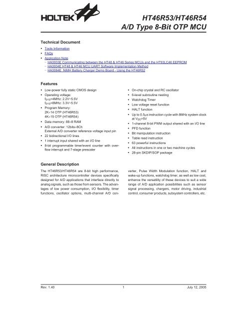
HT46R53/HT46R54 -- A/D Type 8-Bit OTP MCU
HT46R53/HT46R54 -- A/D Type 8-Bit OTP MCU
HT46R53/HT46R54 -- A/D Type 8-Bit OTP MCU

You also want an ePaper? Increase the reach of your titles
YUMPU automatically turns print PDFs into web optimized ePapers that Google loves.
<strong>HT46R53</strong>/<strong>HT46R54</strong><br />
A/D <strong>Type</strong> 8-<strong>Bit</strong> <strong>OTP</strong> <strong>MCU</strong><br />
Technical Document<br />
<br />
<br />
<br />
Tools Information<br />
FAQs<br />
Application Note<br />
HA0003E Communicating between the HT48 & HT46 Series <strong>MCU</strong>s and the HT93LC46 EEPROM<br />
HA0004E HT48 & HT46 <strong>MCU</strong> UART Software Implementation Method<br />
HA0084E NiMH Battery Charger Demo Board - Using the HT46R52<br />
Features<br />
<br />
<br />
<br />
<br />
<br />
<br />
<br />
<br />
Low-power fully static CMOS design<br />
Operating voltage:<br />
f SYS =4MHz: 2.2V~5.5V<br />
f SYS =8MHz: 3.3V~5.5V<br />
Program Memory:<br />
2K14 <strong>OTP</strong> (<strong>HT46R53</strong>)<br />
4K15 <strong>OTP</strong> (<strong>HT46R54</strong>)<br />
Data memory: 888 RAM<br />
A/D converter: 12bits8Ch<br />
External A/D converter reference voltage input pin<br />
22 bidirectional I/O lines<br />
1 interrupt input shared with an I/O line<br />
8-bit programmable timer/event counter with overflow<br />
interrupt and 7-stage prescaler<br />
<br />
<br />
<br />
<br />
<br />
<br />
<br />
<br />
<br />
<br />
<br />
<br />
<br />
On-chip crystal and RC oscillator<br />
6-level subroutine nesting<br />
Watchdog Timer<br />
Low voltage reset function<br />
HALT function<br />
Up to 0.5s instruction cycle with 8MHz system clock<br />
at V DD =5V<br />
1-channel 8-bit PWM output shared with an I/O line<br />
PFD function<br />
<strong>Bit</strong> manipulation instruction<br />
Table read instruction<br />
63 powerful instructions<br />
All instructions in one or two machine cycles<br />
28-pin SKDIP/SOP package<br />
General Description<br />
The <strong>HT46R53</strong>/<strong>HT46R54</strong> are 8-bit high performance,<br />
RISC architecture microcontroller devices specifically<br />
designed for A/D applications that interface directly to<br />
analog signals, such as those from sensors. The advantages<br />
of low power consumption, I/O flexibility, timer<br />
functions, oscillator options, multi-channel A/D converter,<br />
Pulse Width Modulation function, HALT and<br />
wake-up functions, watchdog timer, as well as low cost,<br />
enhance the versatility of these devices to suit a wide<br />
range of A/D application possibilities such as sensor<br />
signal processing, chargers, motor driving, industrial<br />
control, consumer products, subsystem controllers, etc.<br />
Rev. 1.40 1 July 12, 2005
<strong>HT46R53</strong>/<strong>HT46R54</strong><br />
Block Diagram<br />
1 6<br />
2 H C H= <br />
4 <br />
2 H C H= <br />
+ K JA H<br />
5 6 ) + <br />
1 I JHK ? JE <br />
4 A C EI JA H<br />
* 2 2 <br />
7<br />
:<br />
1 JA HHK F J<br />
+ EH? K EJ<br />
, ) 6 )<br />
A HO<br />
1 6 +<br />
6 4 +<br />
6 4<br />
9 , 6 5<br />
9 , 6<br />
2 HA I ? = A H<br />
2 )<br />
2 ) +<br />
2 HJ)<br />
2 HA I ? = A H B5 ; 5<br />
7:<br />
- , 15<br />
9 , 6<br />
6 4<br />
<br />
7:<br />
9 , 6 5 +<br />
B5 ; 5 "<br />
2 ) 2 ) 2 ) ! 2 . ,<br />
2 ) " 6 4 2 ) # 1 6<br />
2 ) $ 2 ) %<br />
) , + L A HJA H<br />
8 , ,<br />
7:<br />
8 4 - .<br />
1 I JHK ? JE <br />
, A ? @ A H<br />
7 :<br />
2 *<br />
2 * +<br />
2 HJ*<br />
2 * ) 2 * % ) %<br />
6 E E C<br />
/ A A H= J H<br />
) 7<br />
5 D EBJA H<br />
5 6 ) 6 7 5<br />
2 +<br />
2 + +<br />
2 HJ+<br />
2 + 2 + "<br />
5 +<br />
5 + <br />
4 - 5<br />
8 , ,<br />
8 5 5<br />
) + +<br />
F JE 4 <br />
6 2 O<br />
2 ,<br />
2 , +<br />
2 HJ,<br />
2 , 2 9 <br />
Pin Assignment<br />
2 ) ! 2 . ,<br />
2 )<br />
2 ) <br />
2 ) <br />
2 , 2 9 <br />
8 4 - .<br />
8 5 5<br />
2 * ) <br />
2 * ) <br />
2 * ) <br />
2 * ! ) !<br />
2 + <br />
2 + <br />
2 +<br />
<br />
!<br />
"<br />
#<br />
$<br />
%<br />
&<br />
'<br />
<br />
<br />
<br />
!<br />
"<br />
&<br />
%<br />
$<br />
#<br />
"<br />
!<br />
<br />
<br />
'<br />
&<br />
%<br />
$<br />
#<br />
2 ) " 6 4<br />
2 ) # 1 6<br />
2 ) $<br />
2 ) %<br />
5 +<br />
5 + <br />
8 , ,<br />
4 - 5<br />
2 * % ) %<br />
2 * $ ) $<br />
2 * # ) #<br />
2 * " ) "<br />
2 + "<br />
2 + !<br />
0 6 " $ 4 # ! 0 6 " 4 # "<br />
& 5 , 12 ) 5 2 )<br />
Rev. 1.40 2 July 12, 2005
<strong>HT46R53</strong>/<strong>HT46R54</strong><br />
Pin Description<br />
Pin Name I/O Options Description<br />
PA0~PA2<br />
PA3/PFD<br />
PA4/TMR<br />
PA5/INT<br />
PA6~PA7<br />
PB0/AN0~<br />
PB7/AN7<br />
I/O<br />
I/O<br />
Pull-high<br />
Wake-up<br />
PA3 or PFD<br />
Pull-high<br />
PC0~PC4 I/O Pull-high<br />
PD0/PWM<br />
OSC1<br />
OSC2<br />
I/O<br />
Pull-high<br />
PD0 or PWM<br />
Bidirectional 8-bit input/output port. Each individual bit on this port can be<br />
configured as a wake-up input by configuration option. Software instructions<br />
determine if the pin is a CMOS output or Schmitt trigger input. Configuration<br />
options determine which pin on this port have pull-high resistors.<br />
The PFD, TMR and external interrupt input are pin-shared with PA3, PA4,<br />
and PA5 respectively.<br />
Bidirectional 8-bit input/output port. Software instructions determine the<br />
CMOS output or Schmitt trigger input with or without pull-high resistor.<br />
Configuration options determine which pin on this port have pull-high resistors.<br />
PB is pin-shared with the A/D input pins. The A/D inputs are selected<br />
via software instructions Once selected as an A/D input, the I/O function<br />
and pull-high resistor functions are disabled automatically.<br />
Bidirectional 5-bit input/output port. Software instructions determine the<br />
CMOS output or Schmitt trigger input with or without pull-high resistor.<br />
Configuration options determine which pin on this port have pull-high resistors.<br />
Bidirectional 1-bit input/output port. Software instructions determine the<br />
CMOS output or Schmitt trigger input with or without pull-high resistor. One<br />
configuration option determines which pin on this port has pull-high resistor.<br />
PD0 is pin-shared with the PWM output selected via configuration option.<br />
OSC1, OSC2 are connected to an external RC network or external crystal<br />
I<br />
O Crystal or RC (determined by configuration option) for the internal system clock. For external<br />
RC system clock operation, OSC2 is an output pin for 1/4 system<br />
clock.<br />
RES I Schmitt trigger reset input, active low.<br />
VDD Positive power supply<br />
VSS Negative power supply, ground<br />
VREF I <br />
A/D Converter Reference Input voltage pins. Connect this pin to the desired<br />
A/D reference voltage.<br />
Absolute Maximum Ratings<br />
Supply Voltage ...........................V SS 0.3V to V SS +6.0V<br />
Input Voltage..............................V SS 0.3V to V DD +0.3V<br />
Storage Temperature ............................50C to125C<br />
Operating Temperature...........................40C to85C<br />
Note: These are stress ratings only. Stresses exceeding the range specified under Absolute Maximum Ratings may<br />
cause substantial damage to the device. Functional operation of this device at other conditions beyond those<br />
listed in the specification is not implied and prolonged exposure to extreme conditions may affect device reliability.<br />
Rev. 1.40 3 July 12, 2005
<strong>HT46R53</strong>/<strong>HT46R54</strong><br />
D.C. Characteristics<br />
Ta=25C<br />
Symbol<br />
Parameter<br />
V DD<br />
V DD Operating Voltage <br />
I DD1<br />
I DD2<br />
Operating Current (Crystal OSC)<br />
Operating Current (RC OSC)<br />
Test Conditions<br />
Conditions<br />
I DD3 Operating Current 5V No load, f SYS=8MHz<br />
ADC disabled<br />
I STB1<br />
I STB2<br />
Standby Current (WDT Enabled)<br />
Standby Current<br />
(WDT & AD Disabled)<br />
Min. Typ. Max. Unit<br />
f SYS =4MHz 2.2 5.5 V<br />
f SYS =8MHz 3.3 5.5 V<br />
3V No load, fSYS =4MHz 0.6 1.5 mA<br />
5V ADC disabled<br />
2 4 mA<br />
3V No load, fSYS =4MHz 0.8 1.5 mA<br />
5V ADC disabled<br />
2.5 4 mA<br />
4 8 mA<br />
3V<br />
No load, system HALT<br />
5 A<br />
5V 10 A<br />
3V<br />
No load, system HALT<br />
1 A<br />
5V 2 A<br />
V IL1<br />
Input Low Voltage for I/O Ports,<br />
TMR and INT<br />
0 0.3V DD V<br />
V IH1<br />
Input High Voltage for I/O Ports,<br />
TMR and INT<br />
0.7V DD V DD V<br />
V IL2 Input Low Voltage (RES) 0 0.4V DD V<br />
V IH2 Input High Voltage (RES) 0.9V DD V DD V<br />
V LVR Low Voltage Reset Voltage Configuration option: 3V 2.7 3 3.3 V<br />
I OL<br />
I OH<br />
I/O Port Sink Current<br />
I/O Port Source Current<br />
3V<br />
VOL =0.1V DD<br />
4 8 mA<br />
5V 10 20 mA<br />
3V<br />
VOH =0.9V DD<br />
2 4 mA<br />
5V 5 10 mA<br />
R PH Pull-high Resistance of I/O Ports<br />
3V<br />
20 60 100 k<br />
<br />
5V 10 30 50 k<br />
V AD A/D Input Voltage 0 V REF V<br />
V REF<br />
ADC Input Reference Voltage<br />
Range<br />
1.2 VDD V<br />
DNL ADC Differential Non-Linear 2 LSB<br />
INL ADC Integral Non-Linear 2.5 4 LSB<br />
RESOLU Resolution 12 <strong>Bit</strong>s<br />
I ADC<br />
Additional Power Consumption<br />
if A/D Converter is Used<br />
3V<br />
0.5 1 mA<br />
<br />
5V 1.5 3 mA<br />
Rev. 1.40 4 July 12, 2005
<strong>HT46R53</strong>/<strong>HT46R54</strong><br />
A.C. Characteristics<br />
Ta=25C<br />
Symbol<br />
f SYS<br />
f TIMER<br />
t WDTOSC<br />
Parameter<br />
System Clock (Crystal OSC)<br />
Timer I/P Frequency (TMR)<br />
Watchdog Oscillator Period<br />
V DD<br />
Test Conditions<br />
Conditions<br />
Min. Typ. Max. Unit<br />
2.2V~5.5V 400 4000 kHz<br />
3.3V~5.5V 400 8000 kHz<br />
2.2V~5.5V 0 4000 kHz<br />
3.3V~5.5V 0 8000 kHz<br />
3V 45 90 180 s<br />
5V 32 65 130 s<br />
t RES External Reset Low Pulse Width 1 s<br />
t SST System Start-up Timer Period Wake-up from HALT 1024 t SYS<br />
t INT Interrupt Pulse Width 1 s<br />
t AD A/D Clock Period 1 s<br />
t ADC A/D Conversion Time 80 t AD<br />
t ADCS A/D Sampling Time 32 t AD<br />
Note: t SYS =1/f SYS<br />
Rev. 1.40 5 July 12, 2005
<strong>HT46R53</strong>/<strong>HT46R54</strong><br />
Functional Description<br />
Execution Flow<br />
The system clock for the microcontroller is derived from<br />
either a crystal or an RC oscillator. The system clock is<br />
internally divided into four non-overlapping clocks. One<br />
instruction cycle consists of 4 system clock cycles.<br />
Instruction fetching and execution are pipelined in such<br />
a way that a fetch and decoding takes an instruction cycle<br />
while execution take the next instruction cycle. The<br />
pipelining scheme causes each instruction to effectively<br />
execute in a cycle. If an instruction changes the program<br />
counter, two cycles are required to complete the instruction.<br />
Program Counter PC<br />
For <strong>HT46R53</strong>, the program counter (PC) is 11 bits wide<br />
and controls the sequence in which the instructions<br />
stored in the program ROM are executed. The contents<br />
of the PC can specify a maximum of 2048 addresses.<br />
For <strong>HT46R54</strong>, the program counter (PC) is 12 bits wide<br />
and controls the sequence in which the instructions<br />
stored in the program ROM are executed. The contents<br />
of the PC can specify a maximum of 4096 addresses.<br />
After accessing a program memory word to fetch an instruction<br />
code, the contents of the program counter are<br />
incremented by one. The program counter then points to<br />
the memory word containing the next instruction code.<br />
When executing a jump instruction, conditional skip execution,<br />
loading register, subroutine call or return from<br />
subroutine, initial reset, internal interrupt, external interrupt<br />
or return from interrupts, the PC manipulates the<br />
program transfer by loading the address corresponding<br />
to each instruction.<br />
The conditional skip is activated by instructions. Once<br />
the condition is met, the next instruction, fetched during<br />
the current instruction execution, is discarded and a<br />
dummy cycle replaces it to get the proper instruction.<br />
Otherwise proceed to the next instruction.<br />
5 O I JA + ? <br />
6 6 6 ! 6 " 6 6 6 ! 6 " 6 6 6 ! 6 "<br />
5 + 4 + O <br />
2 +<br />
2 + 2 + 2 + <br />
. A J? D 1 5 6 2 + <br />
- N A ? K JA 1 5 6 2 + . A J? D 1 5 6 2 + <br />
- N A ? K JA 1 5 6 2 + . A J? D 1 5 6 2 + <br />
- N A ? K JA 1 5 6 2 + <br />
Execution Flow<br />
Mode<br />
Program Counter<br />
*b11 *b10 *b9 *b8 *b7 *b6 *b5 *b4 *b3 *b2 *b1 *b0<br />
Initial Reset 0 0 0 0 0 0 0 0 0 0 0 0<br />
External Interrupt 0 0 0 0 0 0 0 0 0 1 0 0<br />
Timer/Event Counter Overflow 0 0 0 0 0 0 0 0 1 0 0 0<br />
A/D Converter Interrupt 0 0 0 0 0 0 0 0 1 1 0 0<br />
Skip<br />
Program Counter+2<br />
Loading PCL PC11 PC10 PC9 PC8 @7 @6 @5 @4 @3 @2 @1 @0<br />
Jump, Call Branch #11 #10 #9 #8 #7 #6 #5 #4 #3 #2 #1 #0<br />
Return from Subroutine S11 S10 S9 S8 S7 S6 S5 S4 S3 S2 S1 S0<br />
Program Counter<br />
Note:<br />
*b11~*b0: Program counter bits<br />
S11~S0: Stack register bits<br />
#11~#0: Instruction code bits<br />
@7~@0: PCL bits, PC11~PC8: Original PC counter, remain unchanged<br />
For the <strong>HT46R53</strong>, the program counter is 11 bits wide (b0~b10), the b11 column in the table are not applicable.<br />
For the <strong>HT46R54</strong>, the program counter is 12 bits wide, i.e. from b0~b11.<br />
Rev. 1.40 6 July 12, 2005
<strong>HT46R53</strong>/<strong>HT46R54</strong><br />
The lower byte of the PC (PCL) is a readable and<br />
writeable register (06H). Moving data into the PCL performs<br />
a short jump. The destination is within 256 locations.<br />
When a control transfer takes place, an additional<br />
dummy cycle is required.<br />
Program Memory EPROM<br />
The program memory is used to store the program instructions<br />
which are to be executed. It also contains<br />
data, table, and interrupt entries, and is organized into<br />
204814 (<strong>HT46R53</strong>), or 409615 (<strong>HT46R54</strong>) bits, addressed<br />
by the Program Counter and table pointer.<br />
Certain locations in the ROM are reserved for special<br />
usage:<br />
Location 000H<br />
This location is reserved for program initialization. After<br />
a chip reset, the program always begins execution<br />
at location 000H.<br />
Location 004H<br />
This location is reserved for the external interrupt service<br />
program. If the INT input pin is activated, the interrupt<br />
is enabled and the stack is not full, the program<br />
begins execution at this location.<br />
Location 008H<br />
This location is reserved for the timer/event counter<br />
interrupt service program. If a timer interrupt results<br />
from a timer/event counter overflow, and the interrupt<br />
is enabled and the stack is not full, the program begins<br />
execution at location 008H.<br />
Location 00CH<br />
Location 00CH is reserved for the A/D converter interrupt<br />
service program. If an A/D converter interrupt results<br />
from an end of A/D conversion, and if the<br />
interrupt is enabled and the stack is not full, the program<br />
begins execution at location 00CH.<br />
Table location<br />
Any location in the program memory can be used as<br />
look-up tables. The instructions TABRDC [m] (the<br />
0<br />
, A L E? A 1 EJE= E = JE 2 H C H= <br />
0<br />
, A L E? A 1 EJE= E = JE 2 H C H= <br />
" 0<br />
- N JA H = 1 JA HHK F J5 K > H K JE A<br />
" 0<br />
- N JA H = 1 JA HHK F J5 K > H K JE A<br />
& 0<br />
6 E A H- L A J+ K JA H1 JA HHK F J5 K > H K JE A <br />
& 0<br />
6 E A H- L A J+ K JA H1 JA HHK F J5 K > H K JE A <br />
+ 0<br />
) , + L A HJA H1 JA HHK F J5 K > H K JE A<br />
+ 0<br />
) , + L A HJA H1 JA HHK F J5 K > H K JE A<br />
0<br />
" 0<br />
0<br />
" 0<br />
& 0<br />
2 H C H= <br />
A HO<br />
& 0<br />
2 H C H= <br />
A HO<br />
0<br />
. . 0<br />
K F 6 = > A # $ M H@ I <br />
0<br />
. . 0<br />
K F 6 = > A # $ M H@ I <br />
% 0<br />
. 0<br />
% . . 0<br />
K F 6 = > A # $ M H@ I <br />
" > EJI<br />
0 6 " $ 4 # !<br />
JA %<br />
. . . 0<br />
K F 6 = > A # $ M H@ I <br />
# > EJI<br />
0 6 " $ 4 # "<br />
JA .<br />
Program Memory<br />
Instruction<br />
Table Location<br />
b11 b10 b9 b8 b7 b6 b5 b4 b3 b2 b1 b0<br />
TABRDC [m] P11 P10 P9 P8 @7 @6 @5 @4 @3 @2 @1 @0<br />
TABRDL [m] 1 1 1 1 @7 @6 @5 @4 @3 @2 @1 @0<br />
Table Location<br />
Note:<br />
b11~b0: Table location bits<br />
P11~P8: Current program counter bits<br />
@7~@0: Table pointer bits<br />
For the <strong>HT46R53</strong>, since the program counter is 11 bits wide (b0~b10), the b11 columns in the table are not applicable<br />
For the <strong>HT46R54</strong>, the TABRDC program counter is 12 bits wide. From b0~b11<br />
Rev. 1.40 7 July 12, 2005
<strong>HT46R53</strong>/<strong>HT46R54</strong><br />
current page) and TABRDL [m] (the last page)<br />
transfer the contents of the lower-order byte to the<br />
specified data memory, and the higher-order byte to<br />
TBLH (08H). The lower-order byte table pointer TBLP<br />
(07H) are read/write registers, which indicate the table<br />
locations. Before accessing the table, the location has<br />
to be placed in TBLP. The TBLH is read only and cannot<br />
be restored. If the main routine and the ISR (interrupt<br />
service routine) both employ the table read<br />
instruction, the contents of the TBLH in the main routine<br />
are likely to be changed by the table read instruction<br />
used in the ISR. Errors can occur. Given this,<br />
using the table read instruction in the main routine and<br />
the ISR simultaneously should be avoided. However,<br />
if the table read instruction has to be applied in both<br />
main routine and the ISR, the interrupt should be disabled<br />
prior to the table read instruction. It will not be<br />
enabled until the TBLH in the main routine has been<br />
backed-up. All table related instructions require 2 cycles<br />
to complete the operation.<br />
Stack Register STACK<br />
This is a special part of the memory which is used to<br />
save the contents of the program counter only. The<br />
stack is organized into 6 levels and is neither part of the<br />
data nor part of the program space, and is neither readable<br />
nor writeable. The activated level is indexed by the<br />
stack pointer (SP) and is neither readable nor writeable.<br />
At the state of a subroutine call or an interrupt acknowledgment,<br />
the contents of the program counter are<br />
pushed onto the stack. At the end of the subroutine or an<br />
interrupt routine, signaled by a return instruction (RET or<br />
RETI), the program counter is restored to its previous<br />
value from the stack. After a chip reset, the SP will point<br />
to the top of the stack.<br />
If the stack is full and a non-masked interrupt takes<br />
place, the interrupt request flag will be recorded but the<br />
acknowledge signal will be inhibited. When the stack<br />
pointer is decremented (by RET or RETI), the interrupt is<br />
serviced. This feature prevents stack overflow, allowing<br />
the programmer to use the structure more easily. If the<br />
stack is full and a CALL is subsequently executed,<br />
stack overflow occurs and the first entry will be lost (only<br />
the most recent 6 return addresses are stored).<br />
Data Memory RAM<br />
The data memory (RAM) is designed with 1138 bits,<br />
and is divided into two functional groups, namely; special<br />
function registers (258 bits) and general purpose<br />
data memory (888bit) most of which are readable/writable,<br />
although some are read only. Of the two<br />
types of functional groups, the special function registers<br />
consist of an Indirect addressing register 0 (00H), a<br />
Memory pointer register 0 (MP0;01H), an Indirect addressing<br />
register 1 (02H), a Memory pointer register 1<br />
(MP1;03H), an Accumulator (ACC;05H), a Program<br />
counter lower-order byte register (PCL;06H), a Table<br />
pointer (TBLP;07H), a Table higher-order byte register<br />
0<br />
0<br />
0<br />
! 0<br />
" 0<br />
# 0<br />
$ 0<br />
% 0<br />
& 0<br />
' 0<br />
) 0<br />
* 0<br />
+ 0<br />
, 0<br />
- 0<br />
. 0<br />
0<br />
0<br />
0<br />
! 0<br />
" 0<br />
# 0<br />
$ 0<br />
% 0<br />
& 0<br />
' 0<br />
) 0<br />
* 0<br />
+ 0<br />
, 0<br />
- 0<br />
. 0<br />
0<br />
0<br />
0<br />
! 0<br />
" 0<br />
% 0<br />
& 0<br />
% . 0<br />
1 @ EHA ? J) @ @ HA I I E C 4 A C EI JA H<br />
2 <br />
1 @ EHA ? J) @ @ HA I I E C 4 A C EI JA H<br />
2 <br />
) + +<br />
2 + <br />
6 * 2<br />
6 * 0<br />
5 6 ) 6 7 5<br />
1 6 +<br />
6 4<br />
6 4 +<br />
2 )<br />
2 ) +<br />
2 *<br />
2 * +<br />
2 +<br />
2 + +<br />
2 ,<br />
2 , +<br />
2 9 <br />
) , 4 <br />
) , 4 0<br />
) , + 4<br />
) + 5 4<br />
/ A A H= 2 K HF I A<br />
, = J= A HO<br />
& & * O JA I <br />
RAM Mapping<br />
5 F A ? E= 2 K HF I A<br />
, ) 6 ) - 4 ;<br />
7 K I A @<br />
4 A = @ = I <br />
(TBLH;08H), a Status register (STATUS;0AH), an Interrupt<br />
control register (INTC;0BH), a Timer/Event Counter<br />
(TMR:0DH), a Timer/Event Counter control register<br />
(TMRC;0EH), PWM data register (PWM;1AH), the A/D<br />
result lower-order byte register (ADRL;20H), the A/D result<br />
higher-order byte register (ADRH;21H), the A/D<br />
control register (ADCR;22H), the A/D clock setting register<br />
(ACSR;23H), I/O registers (PA;12H, PB;14H,<br />
PC;16H, PD;18H), and I/O control registers (PAC;13H,<br />
PBC;15H, PCC; 17H, PDC;19H). The remaining space<br />
before the 28H is reserved for future expanded usage<br />
and reading these locations will return the result 00H.<br />
The general purpose data memory, addressed from<br />
Rev. 1.40 8 July 12, 2005
<strong>HT46R53</strong>/<strong>HT46R54</strong><br />
28H to 7FH, is used for data and control information under<br />
instruction commands. All of the data memory areas<br />
can handle arithmetic, logic, increment, decrement and<br />
rotate operations directly. Except for some dedicated<br />
bits, each bit in the data memory can be set and reset by<br />
SET [m].i and CLR [m].i. They are also indirectly accessible<br />
through memory pointer registers (MP0;01H or<br />
MP1;03H).<br />
Indirect Addressing Register<br />
Location 00H and 02H are indirect addressing registers<br />
that are not physically implemented. Any read/write operation<br />
of [00H] ([02H]) will access the data memory<br />
pointed to by MP0 (MP1). Reading location 00H (02H)<br />
itself indirectly will return the result 00H. Writing indirectly<br />
results in no operation. The memory pointer registers<br />
(MP0 and MP1) are 7-bit registers.<br />
Accumulator ACC<br />
The accumulator closely relates to ALU operations. It is<br />
also mapped to location 05H of the data memory<br />
which can operate with immediate data. The data movement<br />
between two data memories has to pass through<br />
the accumulator.<br />
Arithmetic and Logic Unit ALU<br />
This circuit performs 8-bit arithmetic and logic operations.<br />
The ALU provides the following functions:<br />
Arithmetic operations (ADD, ADC, SUB, SBC, DAA)<br />
Logic operations (AND, OR, XOR, CPL)<br />
Rotation (RL, RR, RLC, RRC)<br />
Increment and Decrement (INC, DEC)<br />
Branch decision (SZ, SNZ, SIZ, SDZ ....)<br />
The ALU not only saves the results of a data operation<br />
but also changes the status register.<br />
Status Register STATUS<br />
This 8-bit register (0AH) contains the zero flag (Z), carry<br />
flag (C), auxiliary carry flag (AC), overflow flag (OV),<br />
power down flag (PDF), and watchdog time-out flag<br />
(TO). It also records the status information and controls<br />
the operation sequence.<br />
With the exception of the TO and PDF flags, bits in the<br />
status register can be altered by instructions like most<br />
other registers. Any data written into the status register<br />
will not change the TO and PDF flags. Addition operations<br />
related to the status register may give different results<br />
from those intended. The TO flag can be affected<br />
only by system power-up, a WDT time-out or executing<br />
the HALT or CLR WDT instruction. The PDF flag can<br />
be affected only by executing the HALT or CLR WDT<br />
instruction or a system power-up.<br />
The Z, OV, AC, and C flags reflect the status of the latest<br />
operations. On entering the interrupt sequence or executing<br />
the subroutine call, the status register will not be<br />
automatically pushed onto the stack. If the contents of<br />
the status is important, and if the subroutine is likely to<br />
corrupt the status register, the programmer should take<br />
precautions and save it properly.<br />
Interrupts<br />
The device provides an external interrupt, an internal<br />
timer/event counter interrupt, and an A/D converter interrupt.<br />
The interrupt control register (INTC;0BH) contains<br />
the interrupt control bits to set the enable/disable<br />
and the interrupt request flags.<br />
Once an interrupt subroutine is serviced, all the other interrupts<br />
will be blocked (by clearing the EMI bit). This<br />
scheme may prevent any further interrupt nesting. Other<br />
interrupt requests may occur during this interval but only<br />
the interrupt request flag is recorded. If a certain inter-<br />
<strong>Bit</strong> No. Label Function<br />
0 C<br />
1 AC<br />
C is set if an operation results in a carry during an addition operation or if a borrow does not<br />
take place during a subtraction operation; otherwise C is cleared. C is also affected by a rotate<br />
through carry instruction.<br />
AC is set if an operation results in a carry out of the low nibbles in addition or no borrow from<br />
the high nibble into the low nibble in subtraction; otherwise AC is cleared.<br />
2 Z Z is set if the result of an arithmetic or logic operation is zero; otherwise Z is cleared.<br />
3 OV<br />
4 PDF<br />
5 TO<br />
OV is set if an operation results in a carry into the highest-order bit but not a carry out of the<br />
highest-order bit, or vice versa; otherwise OV is cleared.<br />
PDF is cleared by system power-up or executing the CLR WDT instruction. PDF is set by<br />
executing the HALT instruction.<br />
TO is cleared by system power-up or executing the CLR WDT or HALT instruction. TO is<br />
set by a WDT time-out.<br />
6, 7 Unused bit, read as 0<br />
Status (0AH) Register<br />
Rev. 1.40 9 July 12, 2005
<strong>HT46R53</strong>/<strong>HT46R54</strong><br />
rupt requires servicing within the service routine, the<br />
EMI bit and the corresponding bit of the INTC may be<br />
set to allow interrupt nesting. If the stack is full, the interrupt<br />
request will not be acknowledged, even if the related<br />
interrupt is enabled, until the SP is decremented. If<br />
immediate service is desired, the stack must be prevented<br />
from becoming full.<br />
All these kinds of interrupts have a wake-up capability.<br />
As an interrupt is serviced, a control transfer occurs by<br />
pushing the program counter onto the stack, followed by<br />
a branch to a subroutine at specified location in the program<br />
memory. Only the program counter is pushed onto<br />
the stack. If the contents of the register or status register<br />
(STATUS) are altered by the interrupt service program<br />
which corrupts the desired control sequence, the contents<br />
should be saved in advance.<br />
External interrupts are triggered by a high to low transition<br />
of INT and the related interrupt request flag (EIF; bit<br />
4 of the INTC) will be set. When the interrupt is enabled,<br />
the stack is not full and the external interrupt is active, a<br />
subroutine call to location 04H will occur. The interrupt<br />
request flag (EIF) and EMI bits will be cleared to disable<br />
other interrupts.<br />
The internal Timer/Event Counter interrupt is initialized<br />
by setting the Timer/Event Counter interrupt request flag<br />
(TF; bit 5 of the INTC), which is normally caused by a<br />
timer overflow. After the interrupt is enabled, and the<br />
stack is not full, and the TF bit is set, a subroutine call to<br />
location 08H occurs. The related interrupt request flag<br />
(TF) is reset, and the EMI bit is cleared to disable further<br />
maskable interrupts.<br />
The A/D converter interrupt is initialized by setting the<br />
A/D converter request flag (ADF; bit 6 of the INTC),<br />
caused by an end of A/D conversion. When the interrupt<br />
is enabled, the stack is not full and the ADF is set, a subroutine<br />
call to location 0CH will occur. The related interrupt<br />
request flag (ADF) will be reset and the EMI bit<br />
cleared to disable further interrupts.<br />
During the execution of an interrupt subroutine, other interrupt<br />
acknowledgments are held until the RETI instruction<br />
is executed or the EMI bit and the related<br />
interrupt control bit are set to 1 (if the stack is not full). To<br />
return from the interrupt subroutine, RET or RETI<br />
may be invoked. RETI will set the EMI bit to enable an interrupt<br />
service, but RET will not.<br />
Interrupts, occurring in the interval between the rising<br />
edges of two consecutive T2 pulses, will be serviced on<br />
the latter of the two T2 pulses, if the corresponding interrupts<br />
are enabled. In the case of simultaneous requests<br />
the following table shows the priority that is applied.<br />
These can be masked by resetting the EMI bit.<br />
Interrupt Source Priority Vector<br />
External Interrupt 1 04H<br />
Timer/Event Counter Overflow 2 08H<br />
A/D Converter Interrupt 3 0CH<br />
The timer/event counter interrupt request flag (TF), external<br />
interrupt request flag (EIF), A/D converter request<br />
flag (ADF), enable timer/event counter bit (ETI), enable<br />
external interrupt bit (EEI), enable A/D converter interrupt<br />
bit (EADI), and enable master interrupt bit (EMI)<br />
constitute an interrupt control register (INTC) which are<br />
located at 0BH in the data memory. EMI, EEI, ETI, and<br />
EADI are used to control the enabling/disabling of interrupts.<br />
These bits prevent the requested interrupt from<br />
being serviced. Once the interrupt request flags (TF,<br />
EIF, and ADF) are set, they will remain in the INTC register<br />
until the interrupts are serviced or cleared by a software<br />
instruction.<br />
It is recommended that a program does not use the<br />
CALL subroutine within the interrupt subroutine. Interrupts<br />
often occur in an unpredictable manner or<br />
need to be serviced immediately in some applications.<br />
If only one stack is left and enabling the interrupt is not<br />
well controlled, the original control sequence will be damaged<br />
once the CALL operates in the interrupt subroutine.<br />
<strong>Bit</strong> No. Label Function<br />
0 EMI Controls the master (global) interrupt (1= enable; 0= disable)<br />
1 EEI Controls the external interrupt (1= enable; 0= disable)<br />
2 ETI Controls the Timer/Event Counter interrupt (1= enable; 0= disable)<br />
3 EADI Control the A/D converter interrupt (1= enable; 0= disable)<br />
4 EIF External interrupt request flag (1= active; 0= inactive)<br />
5 TF Internal Timer/Event Counter request flag (1= active; 0= inactive)<br />
6 ADF A/D converter request flag (1= active; 0= inactive)<br />
7 <br />
For test mode used only.<br />
Must be written as 0; otherwise may result in unpredictable operation.<br />
INTC (0BH) Register<br />
Rev. 1.40 10 July 12, 2005
<strong>HT46R53</strong>/<strong>HT46R54</strong><br />
Oscillator Configuration<br />
There are two oscillator circuits in the microcontroller.<br />
5 + <br />
" % F .<br />
5 + <br />
5 +<br />
B5 ; 5 " 5 +<br />
+ H O I J= I ? E= J H 4 + I ? E= J H<br />
System Oscillator<br />
Both of them are designed for system clocks, namely<br />
the external RC oscillator and the external Crystal oscillator,<br />
which are determined by options. No matter what<br />
oscillator type is selected, the signal provides the system<br />
clock. The HALT mode stops the system oscillator<br />
and ignores an external signal to conserve power.<br />
If an RC oscillator is used, an external resistor between<br />
OSC1 and VSS is required and the resistance must<br />
range from 30k to 750k. The system clock, divided<br />
by 4, is available on OSC2 with pull-high resistor, which<br />
can be used to synchronize external logic. The RC oscillator<br />
provides the most cost effective solution. However,<br />
the frequency of oscillation may vary with VDD,<br />
temperatures and the chip itself due to process variations.<br />
It is therefore not suitable for timing sensitive operations<br />
where an accurate oscillator frequency is<br />
desired.<br />
If the Crystal oscillator is used, a crystal across OSC1<br />
and OSC2 is needed to provide the feedback and phase<br />
shift required for the oscillator, and no other external<br />
components are required. Instead of a crystal, a resonator<br />
can also be connected between OSC1 and OSC2 to<br />
get a frequency reference, but two external capacitors in<br />
OSC1 and OSC2 are required (If the oscillator can be<br />
disabled by options to conserve power).<br />
The WDT oscillator is a free running on-chip RC oscillator,<br />
and no external components are required. Even if the system<br />
enters the power down mode, the system clock is<br />
stopped, but the WDT oscillator still works with a period of<br />
approximately 65s at 5V. The WDT oscillator can be disabled<br />
by option to conserve power.<br />
8 , ,<br />
Watchdog Timer WDT<br />
The clock source of the WDT is implemented by a dedicated<br />
RC oscillator (WDT oscillator) or instruction clock<br />
(system clock divided by 4) decided by options. This<br />
timer is designed to prevent a software mal-function or<br />
sequence jumping to an unknown location with unpredictable<br />
results. The watchdog timer can be disabled by<br />
an option. If the watchdog timer is disabled, all the executions<br />
related to the WDT result in no operation.<br />
The WDT clock (f S ) is further divided by an internal<br />
counter to give longer watchdog time-outs. In the case<br />
of <strong>HT46R53</strong>/Ht46R54 devices, the division ratio can be<br />
varied by selecting different configuration options to<br />
give 2 12 to 2 15 division ratio range.<br />
Once an internal WDT oscillator (RC oscillator with period<br />
of 65s normally) is selected, it is divided by 2 16 to<br />
get the time-out period of approximately 4.3s. This<br />
time-out period may vary with temperature, VDD and<br />
process variations.<br />
If the WDT oscillator is disabled, the WDT clock may still<br />
come from the instruction clock and operate in the same<br />
manner except that in the HALT state the WDT may stop<br />
counting and lose its protecting purpose. In this situation<br />
the logic can only be restarted by external logic. If the<br />
device operates in a noisy environment, using the<br />
on-chip RC oscillator (WDT OSC) is strongly recommended,<br />
since the HALT will stop the system clock.<br />
The WDT overflow under normal operation will initialize<br />
a chip reset and set the status bit TO. Whereas in the<br />
HALT mode, the overflow will initialize a warm reset<br />
wherein only the Program Counter and SP are reset to<br />
zero. To clear the contents of the WDT, three methods<br />
are adopted; external reset (a low level to RES), software<br />
instructions, or a HALT instruction. The software<br />
instructions include CLR WDT and the other set CLR<br />
WDT1 and CLR WDT2. Of these two types of instruction,<br />
only one can be active depending on the option <br />
CLR WDT times selection option. IftheCLR WDT is<br />
selected (i.e. CLRWDT times equal one), any execution<br />
of the CLR WDT instruction will clear the WDT. In case<br />
CLR WDT1 and CLR WDT2 are chosen (i.e.<br />
CLRWDT times equal two), these two instructions must<br />
+ 4 9 , 6 . = C<br />
+ 4 9 , 6 . = C<br />
+ JH <br />
C E?<br />
H 1 I JHK ? JE I<br />
B5 ; 5 "<br />
9 , 6 I ? E= J H<br />
9 , 6 5 K H? A<br />
+ BEC K H= JE <br />
F JE <br />
B5<br />
& > EJ+ K JA H<br />
B5 &<br />
% > EJ+ K JA H<br />
<br />
+ 4 <br />
9 , 6 6 E A K J<br />
! B5 " B5 # B5 H $ B5 <br />
9 , 6 , EL EI E <br />
+ BEC K H= JE F JE <br />
B5 B5 ! B5 " HB5 #<br />
Watchdog Timer<br />
Rev. 1.40 11 July 12, 2005
<strong>HT46R53</strong>/<strong>HT46R54</strong><br />
be executed to clear the WDT; otherwise, the WDT may<br />
reset the chip because of time-out.<br />
If the WDT division option is selected to f S /2 16 , the WDT<br />
time-out period is fixed to f S /2 16 , because the CLR<br />
WDT or CLR WDT1 and CLR WDT2 instructions will<br />
clear the whole counter of the WDT.<br />
Power Down Operation HALT<br />
The HALT mode is initialized by the HALT instruction<br />
and results in the following...<br />
The system oscillator is turned off but the WDT oscillator<br />
keeps running (if the WDT oscillator or the real<br />
time clock is selected).<br />
The contents of the on-chip RAM and registers remain<br />
unchanged<br />
The WDT and WDT prescaler will be cleared to zero. If<br />
the WDT clock source is from the RTC/WDT oscillator,<br />
the WDT will remain active, and if the WDT clock<br />
source is f SYS /4, the WDT will stop running.<br />
All of the I/O ports maintain their original status<br />
The PDF flag is set and the TO flag is cleared<br />
The system quits the HALT mode by way of an external<br />
reset, an interrupt, an external falling edge signal on port<br />
A or a WDT overflow. An external reset causes a device<br />
initialization and the WDT overflow performs a warm<br />
reset. After examining the TO and PDF flags, the cause<br />
for a chip reset can be determined. The PDF flag is<br />
cleared by system power-up or by executing the CLR<br />
WDT instruction and is set when executing the HALT<br />
instruction. On the other hand, the TO flag is set if the<br />
WDT time-out occurs, and causes a wake-up that only<br />
resets the Program Counter and SP, and leaves the others<br />
in their original status.<br />
The port A wake-up and interrupt methods can be considered<br />
as a continuation of normal execution. Each bit<br />
in port A can be independently selected to wake up the<br />
device by options. Awakening from an I/O port stimulus,<br />
the program resumes execution of the next instruction.<br />
On the other hand, awakening from an interrupt, two sequence<br />
may occur. If the related interrupt is disabled or<br />
the interrupt is enabled but the stack is full, the program<br />
resumes execution at the next instruction. But if the interrupt<br />
is enabled, and the stack is not full, the regular interrupt<br />
response takes place. When an interrupt request<br />
flag is set before entering the HALT status, the system<br />
cannot be awakened using that interrupt. If wake-up<br />
events occur, it takes 1024 t SYS (system clock period) to<br />
resume normal operation. In other words, a dummy period<br />
is inserted after the wake-up. If the wake-up results<br />
from an interrupt acknowledgment, the actual interrupt<br />
subroutine execution is delayed by more than one cycle.<br />
However, if the Wake-up results in the next instruction<br />
execution, the execution will be performed immediately<br />
after the dummy period is finished.<br />
To minimize power consumption, all the I/O pins should<br />
be carefully managed before entering the HALT status.<br />
Reset<br />
There are three ways in which a reset may occur:<br />
RES reset during normal operation<br />
RES reset during HALT<br />
WDT time-out reset during normal operation<br />
The WDT time-out during HALT differs from other chip<br />
reset conditions, for it can perform a warm reset that<br />
resets only the Program Counter and SP, leaving the<br />
other circuits at their original state. Some registers remain<br />
unaffected during any other reset conditions. Most<br />
registers are reset to the initial condition when the reset<br />
conditions are met. Examining the PDF and TO<br />
flags, the program can distinguish between different<br />
chip resets.<br />
TO PDF RESET Conditions<br />
0 0 RES reset during power-up<br />
u u RES reset during normal operation<br />
0 1 RES wake-up HALT<br />
1 u WDT time-out during normal operation<br />
1 1 WDT wake-up HALT<br />
Note: u stands for unchanged<br />
To guarantee that the system oscillator is started and<br />
stabilized, the SST (System Start-up Timer) provides an<br />
extra-delay of 1024 system clock pulses when the system<br />
reset (power-up, WDT time-out or RES reset) or the<br />
system awakes from the HALT state. When a system reset<br />
occurs, the SST delay is added during the reset period.<br />
Any wake-up from the HALT will enable the SST<br />
delay. An extra option load time delay is added during<br />
system reset (Power-up, WDT time-out at normal mode<br />
or RES reset).<br />
The functional unit chip reset status are shown below.<br />
Program Counter<br />
Interrupt<br />
Prescaler, Divider<br />
WDT<br />
Timer/Event Counter<br />
Input/Output Ports<br />
Stack Pointer<br />
000H<br />
Disable<br />
Cleared<br />
Clear. After master reset,<br />
WDT begins counting<br />
Off<br />
Input mode<br />
Points to the top of the stack<br />
Rev. 1.40 12 July 12, 2005
<strong>HT46R53</strong>/<strong>HT46R54</strong><br />
8 , ,<br />
. <br />
8 , ,<br />
4 - 5<br />
J5 5 6 J 2 ,<br />
9<br />
5 5 6 6 E A K J<br />
9<br />
4 - 5<br />
+ D EF 4 A I A J<br />
Reset Timing Chart<br />
. <br />
Note:<br />
Reset Circuit<br />
* Make the length of the wiring, which is connected<br />
to the RES pin as short as possible, to<br />
avoid noise interference.<br />
0 ) 6<br />
4 - 5<br />
5 + <br />
9 , 6<br />
9 , 6<br />
6 E A K J<br />
4 A I A J<br />
5 5 6<br />
> EJ4 EF F A<br />
+ K JA H<br />
- N JA H = <br />
9 = H 4 A I A J<br />
+ @<br />
4 A I A J<br />
2 M A H , A JA ? JE <br />
Reset Configuration<br />
The register states are summarized below:<br />
Register<br />
Reset(Power On)<br />
WDT Time-out<br />
(Normal Operation)<br />
RES Reset<br />
(Normal Operation)<br />
RES Reset<br />
(HALT)<br />
WDT Time-out<br />
(HALT)*<br />
TMR xxxx xxxx xxxx xxxx xxxx xxxx xxxx xxxx uuuu uuuu<br />
TMRC 00-0 1000 00-0 1000 00-0 1000 00-0 1000 uu-u uuuu<br />
Program<br />
Counter<br />
0000H 0000H 0000H 0000H 0000H<br />
MP0 -xxx xxxx -xxx xxxx -xxx xxxx -xxx xxxx -uuu uuuu<br />
MP1 -xxx xxxx -xxx xxxx -xxx xxxx -xxx xxxx -uuu uuuu<br />
ACC xxxx xxxx uuuu uuuu uuuu uuuu uuuu uuuu uuuu uuuu<br />
TBLP xxxx xxxx uuuu uuuu uuuu uuuu uuuu uuuu uuuu uuuu<br />
TBLH xxxx xxxx uuuu uuuu uuuu uuuu uuuu uuuu uuuu uuuu<br />
STATUS --00 xxxx --1u uuuu --uu uuuu --01 uuuu --11 uuuu<br />
INTC -000 0000 -000 0000 -000 0000 -000 0000 -uuu uuuu<br />
PA 1111 1111 1111 1111 1111 1111 1111 1111 uuuu uuuu<br />
PAC 1111 1111 1111 1111 1111 1111 1111 1111 uuuu uuuu<br />
PB 1111 1111 1111 1111 1111 1111 1111 1111 uuuu uuuu<br />
PBC 1111 1111 1111 1111 1111 1111 1111 1111 uuuu uuuu<br />
PC ---1 1111 ---1 1111 ---1 1111 ---1 1111 ---u uuuu<br />
PCC ---1 1111 ---1 1111 ---1 1111 ---1 1111 ---u uuuu<br />
PD ---- ---1 ---- ---1 ---- ---1 ---- ---1 ---- ---u<br />
PDC ---- ---1 ---- ---1 ---- ---1 ---- ---1 ---- ---u<br />
PWM xxxx xxxx xxxx xxxx xxxx xxxx xxxx xxxx uuuu uuuu<br />
ADRL xxxx ---- xxxx ---- xxxx ---- xxxx ---- uuuu ----<br />
ADRH xxxx xxxx xxxx xxxx xxxx xxxx xxxx xxxx uuuu uuuu<br />
ADCR 0100 0000 0100 0000 0100 0000 0100 0000 uuuu uuuu<br />
ACSR ---- --00 ---- --00 ---- --00 ---- --00 ---- --uu<br />
Note:<br />
* stands for warm reset<br />
u stands for unchanged<br />
x stands for unknown<br />
Rev. 1.40 13 July 12, 2005
<strong>HT46R53</strong>/<strong>HT46R54</strong><br />
Timer/Event Counter<br />
Only one timer/event counter (TMR) are implemented in<br />
the microcontroller. The timer/event counter contains an<br />
8-bit programmable count-up counter and the clock may<br />
come from an external source or an internal clock<br />
source. An internal clock source comes from f SYS . The<br />
external clock input allows the user to count external<br />
events, measure time intervals or pulse widths, or to<br />
generate an accurate time base.<br />
There are two registers related to the Timer/event counter;<br />
TMR (0DH), TMRC (0EH). Writing TMR will transfer<br />
the specified data to timer/event counter registers.<br />
Reading the TMR will read the contents of the<br />
timer/event counter. The TMRC is a control register,<br />
which defines the operating mode, counting enable or<br />
disable and an active edge.<br />
The TM0 and TM1 bits define the operation mode. The<br />
event count mode is used to count external events,<br />
which means that the clock source is from an external<br />
(TMR) pin. The timer mode functions as a normal timer<br />
with the clock source coming from the internal selected<br />
clock source. Finally, the pulse width measurement<br />
mode can be used to count the high or low level duration<br />
of the external signal (TMR), and the counting is based<br />
on the internal selected clock source.<br />
In the event count or timer mode, the timer/event counter<br />
starts counting at the current contents in the<br />
timer/event counter and ends at FFH. Once an overflow<br />
occurs, the counter is reloaded from the timer/event<br />
counter preload register, and generates an interrupt request<br />
flag (TF; bit 5 of the INTC ). In the pulse width<br />
measurement mode with the values of the TON and TE<br />
bits equal to 1, after the TMR has received a transient<br />
from low to high (or high to low if the TE bit is 0), it will<br />
start counting until the TMR returns to the original level<br />
and resets the TON. The measured result remains in the<br />
timer/event counter even if the activated transient occurs<br />
again. In other words, only 1-cycle measurement<br />
can be made until the TON is set. The cycle measurement<br />
will re-operate as long as it receives further transient<br />
pulse. In this operation mode, the timer/event<br />
counter begins counting not according to the logic level<br />
but to the transient edges. In the case of counter overflows,<br />
the counter is reloaded from the timer/event counter<br />
register and issues an interrupt request, as in the<br />
other two modes, i.e., event and timer modes.<br />
To enable the counting operation, the Timer ON bit<br />
(TON; bit 4 of the TMRC) should be set to 1. Inthe<br />
pulse width measurement mode, the TON is automatically<br />
cleared after the measurement cycle is completed.<br />
But in the other two modes, the TON can only be reset<br />
by instructions. The overflow of the timer/event counter<br />
is one of the wake-up sources and can also be applied<br />
to a PFD (Programmable Frequency Divider) output at<br />
PA3 by options. No matter what the operation mode is,<br />
writing a 0 to ETI (bit2 of the INTC) disables the related<br />
interrupt service. When the PFD function is selected,<br />
executing SET [PA].3 instruction to enable the<br />
PFD output and executing CLR [PA].3 instruction to<br />
disable the PFD output.<br />
In the case of timer/event counter OFF condition, writing<br />
data to the timer/event counter preload register also reloads<br />
that data to the timer/event counter. But if the<br />
timer/event counter is turn on, data written to the<br />
timer/event counter is kept only in the timer/event counter<br />
preload register. The timer/event counter still continues<br />
its operation until an overflow occurs.<br />
When the timer/event counter (TMR) is read, the clock is<br />
blocked to avoid errors, as this may results in a counting<br />
error. Blocking of the clock issue should be taken into<br />
account by the programmer. It is strongly recommended<br />
to load a desired value into the TMR register first, before<br />
turning on the related timer/event counter, for proper operation<br />
since the initial value of TMR is unknown. Due to<br />
the timer/event scheme, the programmer should pay<br />
special attention on the instruction to enable then disable<br />
the timer for the first time, whenever there is a need<br />
to use the timer/event function, to avoid unpredictable<br />
result. After this procedure, the timer/event function can<br />
be operated normally.<br />
The bit0~bit2 of the TMRC can be used to define the<br />
pre-scaling stages of the internal clock sources of the<br />
timer/event counter. The definitions are as shown. The<br />
overflow signal of the timer/event counter can be used<br />
to generate the PFD signal. The timer prescaler is also<br />
used as the PWM counter.<br />
, = J= * K I<br />
2 HA = @ 4 A C EI JA H<br />
4 A = @<br />
2 5 + 2 5 + <br />
6 6 <br />
B5 ; 5<br />
6 4 E F K J<br />
& I J= C A F HA I ? = A H<br />
6 E A H- L A J+ K JA H<br />
@ A + JH <br />
6 <br />
6 E A H- L A J<br />
+ K JA H<br />
& * EJ6 E A H- L A J+ K JA H<br />
<br />
L A HB M<br />
J 1 JA HHK F J<br />
2 . ,<br />
6 -<br />
8-<strong>Bit</strong> Timer/Event Counter Structure<br />
Rev. 1.40 14 July 12, 2005
<strong>HT46R53</strong>/<strong>HT46R54</strong><br />
<strong>Bit</strong> No. Label Function<br />
0<br />
1<br />
2<br />
PSC0<br />
PSC1<br />
PSC2<br />
Defines the prescaler stages, PSC2, PSC1, PSC0=<br />
000: f INT =f SYS<br />
001: f INT =f SYS /2<br />
010: f INT =f SYS /4<br />
011: f INT =f SYS /8<br />
100: f INT =f SYS /16<br />
101: f INT =f SYS /32<br />
110: f INT =f SYS /64<br />
111: f INT =f SYS /128<br />
3 TE<br />
Defines the TMR active edge of the timer/event counter:<br />
In Event Counter Mode (TM1,TM0)=(0,1):<br />
1:count on falling edge;<br />
0:count on rising edge<br />
In Pulse Width measurement mode (TM1,TM0)=(1,1):<br />
1: start counting on the rising edge, stop on the falling edge;<br />
0: start counting on the falling edge, stop on the rising edge<br />
4 TON Enable/disable timer counting (0=disable; 1=enable)<br />
5 Unused bit, read as 0<br />
6<br />
7<br />
TM0<br />
TM1<br />
Defines the operating mode, TM1, TM0:<br />
01=Event count mode (external clock)<br />
10=Timer mode (internal clock)<br />
11=Pulse width measurement mode<br />
00=Unused<br />
TMRC (0EH) Register<br />
Input/Output Ports<br />
There are 22 bidirectional input/output lines in the<br />
microcontroller, labeled as PA, PB, PC and PD, which<br />
are mapped to the data memory of [12H], [14H], [16H]<br />
and [18H] respectively. All of these I/O ports can be<br />
used for input and output operations. For input operation,<br />
these ports are non-latching, that is, the inputs<br />
must be ready at the T2 rising edge of instruction MOV<br />
A,[m] (m=12H, 14H, 16H or 18H). For output operation,<br />
all the data is latched and remains unchanged until the<br />
output latch is rewritten.<br />
8 , ,<br />
, = J= * K I<br />
+ JH * EJ<br />
, 3<br />
2 7<br />
9 HEJA + JH 4 A C EI JA H<br />
+ D EF 4 A I A J<br />
4 A = @ + JH 4 A C EI JA H<br />
9 HEJA , = J= 4 A C EI JA H<br />
+ 3<br />
5<br />
, = J= * EJ<br />
, 3<br />
+ <br />
3<br />
5<br />
<br />
7<br />
:<br />
2 ) 2 )<br />
2 ) ! 2 . ,<br />
2 ) " 6 4<br />
2 ) # 1 6<br />
2 ) $<br />
2 ) %<br />
2 * ) 2 * % ) %<br />
2 + 2 + "<br />
2 , 2 9 <br />
2 ) ! 2 . , <br />
H2 , 2 9 <br />
4 A = @ , = J= 4 A C EI JA H<br />
5 O I JA 9 = A K F<br />
2 ) O <br />
1 6 B H2 ) # O<br />
<br />
7:<br />
- 2 . , H2 9 <br />
9 = A K F F JE <br />
Input/Output Ports<br />
Rev. 1.40 15 July 12, 2005
<strong>HT46R53</strong>/<strong>HT46R54</strong><br />
Each I/O line has its own control register (PAC, PBC,<br />
PCC, PDC) to control the input/output configuration.<br />
With this control register, CMOS output or Schmitt trigger<br />
input with or without pull-high resistor structures can<br />
be reconfigured dynamically under software control. To<br />
function as an input, the corresponding latch of the control<br />
register must write 1. The input source also depends<br />
on the control register. If the control register bit is<br />
1, the input will read the pad state. If the control register<br />
bit is 0, the contents of the latches will move to the<br />
internal bus. The latter is possible in the<br />
read-modify-write instruction.<br />
For output function, CMOS is the only configuration.<br />
These control registers are mapped to locations 13H,<br />
15H, 17H and 19H.<br />
After a chip reset, these input/output lines remain at high<br />
levels or floating state (dependent on pull-high options).<br />
Each bit of these input/output latches can be set or<br />
cleared by SET [m].i and CLR [m].i (m=12H, 14H,<br />
16H or 18H) instructions.<br />
Some instructions first input data and then follow the<br />
output operations. For example, SET [m].i, CLR<br />
[m].i, CPL [m], CPLA [m] read the entire port states<br />
into the CPU, execute the defined operations<br />
(bit-operation), and then write the results back to the<br />
latches or the accumulator.<br />
Each line of port A has the capability of waking-up the<br />
device. Each I/O port has a pull-high option. Once the<br />
pull-high option is selected, the I/O port has a pull-high<br />
resistor, otherwise, theres none. Take note that a nonpull-high<br />
I/O port operating in input mode will cause a<br />
floating state.<br />
The PA3, PA4 and PA5 are pin-shared with PFD, TMR<br />
and INT pins respectively.<br />
If the PFD option is selected, the output signal in output<br />
mode of PA3 will be the PFD signal generated by the<br />
timer/event counter overflow signal. The input mode always<br />
remain in its original functions. Once the PFD option<br />
is selected, the PFD output signal is controlled by<br />
the PA3 data register only. The I/O functions of PA3 are<br />
shown below.<br />
I/O<br />
Mode<br />
PA3<br />
Note:<br />
I/P<br />
(Normal)<br />
Logical<br />
Input<br />
O/P<br />
(Normal)<br />
Logical<br />
Output<br />
I/P<br />
(PFD)<br />
Logical<br />
Input<br />
O/P<br />
(PFD)<br />
PFD<br />
(Timer on)<br />
The PFD frequency is the timer/event counter<br />
overflow frequency divided by 2.<br />
The definitions of the PFD control signal and PFD output<br />
frequency are listed in the following table.<br />
Timer<br />
Timer<br />
PA3 Data PA3 Pad<br />
Preload<br />
Register State<br />
Value<br />
Frequency<br />
OFF X 0 0 X<br />
OFF X 1 U X<br />
ON N 0 0 X<br />
Note:<br />
ON N 1 PFD f INT /(2(256-N))<br />
X stands for unused<br />
U stands for unknown<br />
N is the preload value for the timer/event<br />
counter<br />
f TMR is the input clock frequency for the<br />
timer/event counter<br />
The PB can also be used as A/D converter inputs. The<br />
A/D function will be described later. There is a PWM<br />
function shared with PD0. If the PWM function is enabled,<br />
the PWM signal will appear on PD0 (if PD0 is operating<br />
in output mode). The I/O functions of PD0 are as<br />
shown.<br />
I/O<br />
Mode<br />
PD0<br />
I/P<br />
(Normal)<br />
Logical<br />
Input<br />
O/P<br />
(Normal)<br />
Logical<br />
Output<br />
I/P<br />
(PWM)<br />
Logical<br />
Input<br />
O/P<br />
(PWM)<br />
PWM<br />
It is recommended that unused or not bonded out I/O<br />
lines should be set as output pins by software instruction<br />
to avoid consuming power under input floating state.<br />
PWM<br />
The microcontroller provides one channel PWM output<br />
shared with PD0. The PWM supports (7+1) or (6+2)<br />
modes which are selected by configuration option. The<br />
PWM channel has their data register denoted as<br />
PWM(1AH). The frequency source of the PWM counter<br />
comes from f SYS . The PWM register is an 8-bit register.<br />
The waveforms of the PWM outputs are as shown.<br />
Once the PD0 are selected as the PWM outputs and the<br />
output function of the PD0 are enabled (PDC.0= 0),<br />
writing 1 to PD0 data register will enable the PWM output<br />
function and writing 0 will force the PD0 to stay at<br />
0.<br />
A (6+2) bits mode PWM cycle is divided into four modulation<br />
cycles (modulation cycle 0~modulation cycle 3).<br />
Each modulation cycle has 64 PWM input clock period.<br />
In a (6+2) bit PWM function, the contents of the PWM<br />
Rev. 1.40 16 July 12, 2005
<strong>HT46R53</strong>/<strong>HT46R54</strong><br />
register is divided into two groups. Group 1 of the PWM<br />
register is denoted by DC which is the value of<br />
PWM.7~PWM.2. The group 2 is denoted by AC which is<br />
the value of PWM.1~PWM.0. In a (6+2) bits mode PWM<br />
cycle, the duty cycle of each modulation cycle is shown<br />
in the table.<br />
Parameter AC (0 3) Duty Cycle<br />
Modulation cycle i<br />
(i=0~3)<br />
iAC<br />
i AC<br />
DC+1<br />
64<br />
DC<br />
64<br />
A (7+1) bits mode PWM cycle is divided into two modulation<br />
cycles (modulation cycle0~modulation cycle 1).<br />
Each modulation cycle has 128 PWM input clock period.<br />
In a (7+1) bits PWM function, the contents of the PWM<br />
register is divided into two groups. Group 1 of the PWM<br />
register is denoted by DC which is the value of<br />
PWM.7~PWM.1. The group 2 is denoted by AC which is<br />
the value of PWM.0. In a (7+1) bits mode PWM cycle,<br />
the duty cycle of each modulation cycle is shown in the<br />
table.<br />
Parameter AC (0 1) Duty Cycle<br />
Modulation cycle i<br />
(i=0~1)<br />
iAC<br />
i AC<br />
DC+1<br />
128<br />
DC<br />
128<br />
The modulation frequency, cycle frequency and cycle<br />
duty of the PWM output signal are summarized in the<br />
following table.<br />
PWM<br />
Modulation Frequency<br />
f SYS /64 for (6+2) bits mode<br />
f SYS /128 for (7+1) bits mode<br />
PWM Cycle PWM Cycle<br />
Frequency Duty<br />
f SYS /256<br />
[PWM]/256<br />
B5 ; 5 <br />
2 9 <br />
2 9 <br />
# $ "<br />
# $ " # $ " # $ "<br />
# $ "<br />
2 9 <br />
2 9 <br />
$ $ "<br />
# $ "<br />
# $ "<br />
# $ "<br />
$ $ "<br />
2 9 <br />
2 9 <br />
$ $ "<br />
$ $ "<br />
# $ "<br />
# $ "<br />
$ $ "<br />
2 9 !<br />
2 9 <br />
$ $ "<br />
$ $ "<br />
$ $ " # $ "<br />
$ $ "<br />
2 9 @ K = JE F A HE @ $ " B5 ; 5<br />
@ K = JE ? O ? A <br />
@ K = JE ? O ? A @ K = JE ? O ? A @ K = JE ? O ? A ! @ K = JE ? O ? A <br />
2 9 ? O ? A # $ B5 ; 5<br />
(6 2) PWM Mode<br />
B5 ; 5 <br />
2 9 <br />
2 9 <br />
# &<br />
# &<br />
# &<br />
2 9 <br />
2 9 <br />
# &<br />
# &<br />
# &<br />
2 9 <br />
2 9 <br />
# &<br />
# &<br />
# &<br />
2 9 !<br />
2 9 <br />
# &<br />
# &<br />
# &<br />
2 9 @ K = JE F A HE @ & B5 ; 5<br />
@ K = JE ? O ? A <br />
@ K = JE ? O ? A <br />
@ K = JE ? O ? A <br />
2 9 ? O ? A # $ B5 ; 5<br />
(7 1) PWM Mode<br />
Rev. 1.40 17 July 12, 2005
<strong>HT46R53</strong>/<strong>HT46R54</strong><br />
A/D Converter<br />
The 8 channels 12-bit resolution A/D converter are implemented<br />
in this microcontroller.<br />
The A/D converter contains 4 special registers which<br />
are; ADRL (20H), ADRH (21H), ADCR (22H) and ACSR<br />
(23H). The ADRH and ADRL are A/D result register<br />
higher-order byte and lower-order byte and are<br />
read-only. After the A/D conversion is completed, the<br />
ADRH and ADRL should be read to get the conversion<br />
result data. The ADCR is an A/D converter control register,<br />
which defines the A/D channel number, analog<br />
channel select, start A/D conversion control bit and the<br />
end of A/D conversion flag. If the users want to start an<br />
A/D conversion, define PB configuration, select the converted<br />
analog channel, and give START bit a raising<br />
edge and falling edge (010). At the end of A/D conversion,<br />
the EOCB bit is cleared and an A/D converter<br />
interrupt occurs (if the A/D converter interrupt is enabled).<br />
The ACSR is A/D clock setting register, which is<br />
used to select the A/D clock source.<br />
The A/D converter control register is used to control the<br />
A/D converter. The bit2~bit0 of the are used to select an<br />
analog input channel. There are a total of eight channels<br />
to select. The bit5~bit3 of the ADCR are used to set PB<br />
configurations. PB can be an analog input or as digital<br />
I/O line determined by these 3 bits. Once a PB line is selected<br />
as an analog input, the I/O functions and pull-high<br />
resistor of this I/O line are disabled and the A/D converter<br />
circuit is powered on. The EOCB bit (bit6 of the<br />
ADCR) is end of A/D conversion flag. Check this bit to<br />
know when the A/D conversion is completed.<br />
The START bit of the ADCR is used to begin the conversion<br />
of the A/D converter. Giving START bit a rising edge<br />
and falling edge means that the A/D conversion has<br />
started. In order to ensure that the A/D conversion is<br />
completed, the START should remain at 0 until the<br />
EOCB is cleared to 0 (end of A/D conversion). <strong>Bit</strong> 7 of<br />
the ACSR register is used for test purposes only and<br />
must not be used for other purposes by the application<br />
program. <strong>Bit</strong>1 and bit0 of the ACSR register are used to<br />
select the A/D clock source.<br />
When the A/D conversion has completed, the A/D interrupt<br />
request flag will be set. The EOCB bit is set to 1<br />
when the START bit is set from 0 to 1.<br />
Important Note for A/D initialisation:<br />
Special care must be taken to initialise the A/D converter<br />
each time the Port B A/D channel selection bits<br />
are modified, otherwise the EOCB flag may be in an undefined<br />
condition. An A/D initialisation is implemented<br />
by setting the START bit high and then clearing it to zero<br />
within 10 instruction cycles of the Port B channel selection<br />
bits being modified. Note that if the Port B channel<br />
selection bits are all cleared to zero then an A/D initialisation<br />
is not required.<br />
<strong>Bit</strong> No. Label<br />
0<br />
1<br />
Function<br />
Selects the A/D converter clock source<br />
00= system clock/2<br />
ADCS0<br />
01= system clock/8<br />
ADCS1<br />
10= system clock/32<br />
11= undefined<br />
2~6 Unused bit, read as 0<br />
7 TEST For test mode used only<br />
<strong>Bit</strong> No. Label<br />
0<br />
1<br />
2<br />
3<br />
4<br />
5<br />
ACS0<br />
ACS1<br />
ACS2<br />
PCR0<br />
PCR1<br />
PCR2<br />
6 EOCB<br />
7 START<br />
ACSR (23H) Register<br />
Function<br />
Defines the analog channel select<br />
Defines the port B configuration select.<br />
If PCR0, PCR1 and PCR2 are all<br />
zero, the ADC circuit is powered off to<br />
reduce power consumption<br />
Indicates end of A/D conversion.<br />
(0= end of A/D conversion)<br />
Each time bits 3~5 change state the<br />
A/D should be initialised by issuing a<br />
START signal, otherwise the EOCB<br />
flag may have an undefined condition.<br />
See Important note for A/D initialisation.<br />
Starts the A/D conversion.<br />
010= Start<br />
01= Reset A/D converter and set<br />
EOCB to 1.<br />
ADCR (22H) Register<br />
ACS2 ACS1 ACS0 Analog Channel<br />
0 0 0 AN0<br />
0 0 1 AN1<br />
0 1 0 AN2<br />
0 1 1 AN3<br />
1 0 0 AN4<br />
1 0 1 AN5<br />
1 1 0 AN6<br />
1 1 1 AN7<br />
Analog Input Channel Selection<br />
Register <strong>Bit</strong>7 <strong>Bit</strong>6 <strong>Bit</strong>5 <strong>Bit</strong>4 <strong>Bit</strong>3 <strong>Bit</strong>2 <strong>Bit</strong>1 <strong>Bit</strong>0<br />
ADRL<br />
D3 D2 D1 D0 0 0 0 0<br />
(20H)<br />
ADRH<br />
D11 D10 D9 D8 D7 D6 D5 D4<br />
(21H)<br />
Note:<br />
D0~D11 is A/D conversion result data bit<br />
LSB~MSB.<br />
Rev. 1.40 18 July 12, 2005
<strong>HT46R53</strong>/<strong>HT46R54</strong><br />
PCR2 PCR1 PCR0 7 6 5 4 3 2 1 0<br />
0 0 0 PB7 PB6 PB5 PB4 PB3 PB2 PB1 PB0<br />
0 0 1 PB7 PB6 PB5 PB4 PB3 PB2 PB1 AN0<br />
0 1 0 PB7 PB6 PB5 PB4 PB3 PB2 AN1 AN0<br />
0 1 1 PB7 PB6 PB5 PB4 PB3 AN2 AN1 AN0<br />
1 0 0 PB7 PB6 PB5 PB4 AN3 AN2 AN1 AN0<br />
1 0 1 PB7 PB6 PB5 AN4 AN3 AN2 AN1 AN0<br />
1 1 0 PB7 PB6 AN5 AN4 AN3 AN2 AN1 AN0<br />
1 1 1 AN7 AN6 AN5 AN4 AN3 AN2 AN1 AN0<br />
Port B Configuration<br />
E E K A E I JHK ? JE ? O ? A A A @ A @ = N E K JA E I JHK ? JE ? O ? A I = M A @<br />
5 6 ) 4 6<br />
- + *<br />
) , I = F E C JE A<br />
J) , + 5 <br />
) , I = F E C JE A<br />
J) , + 5 <br />
) , I = F E C JE A<br />
J) , + 5 <br />
2 + 4 <br />
2 + 4 <br />
) + 5 <br />
) + 5 <br />
*<br />
*<br />
2 M A H <br />
4 A I A J<br />
, A BE A 2 * ? BEC K H= JE <br />
5 A A ? J= = C ? D = A <br />
*<br />
*<br />
5 J= HJ B) ,<br />
? L A HI E <br />
4 A I A J) ,<br />
? L A HJA H<br />
J) , +<br />
) , ? L A HI E JE A<br />
*<br />
*<br />
5 J= HJ B) ,<br />
? L A HI E <br />
4 A I A J) ,<br />
? L A HJA H<br />
- @ B) ,<br />
? L A HI E <br />
J) , +<br />
) , ? L A HI E JE A<br />
*<br />
*<br />
5 J= HJ B) ,<br />
? L A HI E <br />
4 A I A J) ,<br />
? L A HJA H<br />
- @ B) ,<br />
? L A HI E <br />
- @ B) ,<br />
? L A HI E <br />
J) , +<br />
) , ? L A HI E JE A<br />
*<br />
2 * F HJI A JK F = I 1 I<br />
) , ? L A HJA HEI F M A HA @ BB<br />
J HA @ K ? A F M A H? I K F JE <br />
@ J? = HA<br />
JA ) , ? ? K I J> A B5 ; 5 B5 ; 5 & HB5 ; 5 !<br />
J) , + 5 ! J) ,<br />
J) , + & J) ,<br />
A/D Conversion Timing<br />
The following two programming examples illustrate how to setup and implement an A/D conversion. In the first example,<br />
the method of polling the EOCB bit in the ADCR register is used to detect when the conversion cycle is complete,<br />
whereas in the second example, the A/D interrupt is used to determine when the conversion is complete.<br />
Example: using EOCB Polling Method to detect end of conversion<br />
clr EADI ; disable ADC interrupt<br />
mov a,00000001B<br />
mov ACSR,a ; setup the ACSR register to select f SYS /8 as the A/D clock<br />
mov a,00100000B ; setup ADCR register to configure Port PB0~PB3 as A/D inputs<br />
mov ADCR,a ; and select AN0 to be connected to the A/D converter<br />
:<br />
: ; As the Port B channel bits have changed the following START<br />
; signal (0-1-0) must be issued within 10 instruction cycles<br />
:<br />
Start_conversion:<br />
clr START<br />
set START ; reset A/D<br />
clr START ; start A/D<br />
Polling_EOC:<br />
sz EOCB ; poll the ADCR register EOCB bit to detect end of A/D conversion<br />
jmp polling_EOC ; continue polling<br />
mov a,ADRH ; read conversion result high byte value from the ADRH register<br />
mov adrh_buffer,a ; save result to user defined memory<br />
mov a,ADRL ; read conversion result low byte value from the ADRL register<br />
mov adrl_buffer,a ; save result to user defined memory<br />
:<br />
:<br />
jmp start_conversion ; start next A/D conversion<br />
Rev. 1.40 19 July 12, 2005
<strong>HT46R53</strong>/<strong>HT46R54</strong><br />
Example: using Interrupt Method to detect end of conversion<br />
clr EADI ; disable ADC interrupt<br />
mov a,00000001B<br />
mov ACSR,a ; setup the ACSR register to select f SYS /8 as the A/D clock<br />
mov a,00100000B ; setup ADCR register to configure Port PB0~PB3 as A/D inputs<br />
mov ADCR,a ; and select AN0 to be connected to the A/D converter<br />
:<br />
; As the Port B channel bits have changed the following START<br />
; signal (0-1-0) must be issued within 10 instruction cycles<br />
:<br />
Start_conversion:<br />
clr START<br />
set START ; reset A/D<br />
clr START ; start A/D<br />
clr ADF ; clear ADC interrupt request flag<br />
set EADI ; enable ADC interrupt<br />
set EMI ; enable global interrupt<br />
:<br />
:<br />
:<br />
; ADC interrupt service routine<br />
ADC_ISR:<br />
mov acc_stack,a ; save ACC to user defined memory<br />
mov a,STATUS<br />
mov status_stack,a ; save STATUS to user defined memory<br />
:<br />
:<br />
mov a,ADRH ; read conversion result high byte value from the ADRH register<br />
mov adrh_buffer,a ; save result to user defined register<br />
mov a,ADRL ; read conversion result low byte value from the ADRL register<br />
mov adrl_buffer,a ; save result to user defined register<br />
clr START<br />
set START ; reset A/D<br />
clr START ; start A/D<br />
:<br />
:<br />
EXIT_INT_ISR:<br />
mov a,status_stack<br />
mov STATUS,a ; restore STATUS from user defined memory<br />
mov a,acc_stack ; restore ACC from user defined memory<br />
reti<br />
Low Voltage Reset LVR<br />
There is a low voltage reset circuit (LVR) implemented in<br />
the microcontrollers. The function can be enabled/disabled<br />
by options.<br />
If the supply voltage of the device is within the range<br />
0.9V~V LVR such as changing a battery, the LVR will automatically<br />
reset the device internally.<br />
The LVR includes the following specifications:<br />
The low voltage (0.9V~V LVR ) has to remain in their<br />
original state to exceed 1ms. If the low voltage state<br />
does not exceed 1ms, the LVR will ignore it and do not<br />
perform a reset function.<br />
The LVR uses the OR function with the external RES<br />
signal to perform chip reset.<br />
The relationship between V DD and V LVR is shown below.<br />
8 , , 8 2 4<br />
# # 8 # # 8<br />
! 8<br />
8<br />
8 8 4<br />
' 8<br />
Note: V OPR is the voltage range for proper chip<br />
operation at 4MHz system clock.<br />
Rev. 1.40 20 July 12, 2005
<strong>HT46R53</strong>/<strong>HT46R54</strong><br />
8 , ,<br />
# # 8<br />
8 8 4<br />
8 4 , A JA ? J8 J= C A<br />
' 8<br />
8<br />
4 A I A J5 EC = <br />
4 A I A J<br />
H = F A H= JE <br />
4 A I A J<br />
<br />
<br />
Low Voltage Reset<br />
Note:<br />
*1: To make sure that the system oscillator has stabilized, the SST provides an extra delay of 1024 system<br />
clock pulses before entering the normal operation.<br />
*2: Since low voltage state has to be maintained in its original state for over 1ms, therefore after 1ms delay,<br />
the device enters the reset mode.<br />
Options<br />
The following shows kinds of options in the device. ALL the options must be defined to ensure having a proper functioning<br />
system.<br />
Options<br />
OSC type selection.<br />
This option is to decide if an RC or crystal oscillator is chosen as system clock.<br />
WDT source selection.<br />
There are three types of selection: on-chip RC oscillator, instruction clock or disable the WDT.<br />
CLRWDT times selection.<br />
This option defines how to clear the WDT by instruction. One time means that the CLR WDT instruction can clear<br />
the WDT. Two times means only if both of the CLR WDT1 and CLR WDT2 instructions have been executed,<br />
then WDT can be cleared.<br />
Wake-up selection.<br />
This option defines the wake-up function activity. External I/O pins (PA only) all have the capability to wake-up the<br />
chip from a HALT by a falling edge. (<strong>Bit</strong> option)<br />
Pull-high selection.<br />
This option is to decide whether a pull-high resistance is visible or not in the input mode of the I/O ports. PA is bit option;<br />
PB, PC and PD are port option.<br />
PFD selection.<br />
PA3: Level output or PFD output.<br />
PWM selection: (7+1) or (6+2) mode<br />
PD0: level output or PWM output<br />
WDT time-out period selection.<br />
There are four types of selection: WDT clock source divided by 2 12 ,2 13 ,2 14 and 2 15<br />
LVR selection.<br />
Enable or disable LVR function.<br />
Rev. 1.40 21 July 12, 2005
<strong>HT46R53</strong>/<strong>HT46R54</strong><br />
Application Circuits<br />
8 , ,<br />
9<br />
.<br />
5 +<br />
+ EH? K EJ<br />
.<br />
9<br />
.<br />
5 A A 4 EC D J5 E@ A<br />
8 , ,<br />
4 - 5<br />
8 5 5<br />
5 + <br />
5 +<br />
2 ) 2 )<br />
2 ) ! 2 . ,<br />
2 ) " 6 4<br />
2 ) # 1 6<br />
2 ) $ 2 ) %<br />
2 * ) <br />
<br />
2 * % ) %<br />
2 + 2 + "<br />
2 , 2 9 <br />
8 , ,<br />
" % F .<br />
4 5 +<br />
B5 ; 5 "<br />
+ <br />
+<br />
4 <br />
5 + <br />
5 +<br />
5 + <br />
5 +<br />
4 + 5 O I JA I ? E= J H<br />
! 9 4 5 + % # 9<br />
+ H O I J= 5 O I JA I ? E= J H<br />
. HJD A L = K A I <br />
I A A J= > A > A M<br />
0 6 " $ 4 # ! 0 6 " $ 4 # "<br />
5 + + EH ? K EJ<br />
The following table shows the C1, C2 and R1 values corresponding to the different crystal values. (For reference only)<br />
Crystal or Resonator C1, C2 R1<br />
4MHz Crystal 0pF 10k<br />
4MHz Resonator 10pF 12k<br />
3.58MHz Crystal 0pF 10k<br />
3.58MHz Resonator 25pF 10k<br />
2MHz Crystal & Resonator 25pF 10k<br />
1MHz Crystal 35pF 27k<br />
480kHz Resonator 300pF 9.1k<br />
455kHz Resonator 300pF 10k<br />
429kHz Resonator 300pF 10k<br />
The function of the resistor R1 is to ensure that the oscillator will switch off should low voltage conditions occur.<br />
Such a low voltage, as mentioned here, is one which is less than the lowest value of the <strong>MCU</strong> operating voltage.<br />
Note however that if the LVR is enabled then R1 can be removed.<br />
Note:<br />
The resistance and capacitance for reset circuit should be designed in such a way as to ensure that the VDD is<br />
stable and remains within a valid operating voltage range before bringing RES to high.<br />
* Make the length of the wiring, which is connected to the RES pin as short as possible, to avoid noise<br />
interference.<br />
Rev. 1.40 22 July 12, 2005
<strong>HT46R53</strong>/<strong>HT46R54</strong><br />
Instruction Set Summary<br />
Mnemonic<br />
Arithmetic<br />
ADD A,[m]<br />
ADDM A,[m]<br />
ADD A,x<br />
ADC A,[m]<br />
ADCM A,[m]<br />
SUB A,x<br />
SUB A,[m]<br />
SUBM A,[m]<br />
SBC A,[m]<br />
SBCM A,[m]<br />
DAA [m]<br />
Logic Operation<br />
AND A,[m]<br />
OR A,[m]<br />
XOR A,[m]<br />
ANDM A,[m]<br />
ORM A,[m]<br />
XORM A,[m]<br />
AND A,x<br />
OR A,x<br />
XOR A,x<br />
CPL [m]<br />
CPLA [m]<br />
Increment & Decrement<br />
INCA [m]<br />
INC [m]<br />
DECA [m]<br />
DEC [m]<br />
Rotate<br />
RRA [m]<br />
RR [m]<br />
RRCA [m]<br />
RRC [m]<br />
RLA [m]<br />
RL [m]<br />
RLCA [m]<br />
RLC [m]<br />
Data Move<br />
MOV A,[m]<br />
MOV [m],A<br />
MOV A,x<br />
<strong>Bit</strong> Operation<br />
CLR [m].i<br />
SET [m].i<br />
Description<br />
Add data memory to ACC<br />
Add ACC to data memory<br />
Add immediate data to ACC<br />
Add data memory to ACC with carry<br />
Add ACC to data memory with carry<br />
Subtract immediate data from ACC<br />
Subtract data memory from ACC<br />
Subtract data memory from ACC with result in data memory<br />
Subtract data memory from ACC with carry<br />
Subtract data memory from ACC with carry and result in data memory<br />
Decimal adjust ACC for addition with result in data memory<br />
AND data memory to ACC<br />
OR data memory to ACC<br />
Exclusive-OR data memory to ACC<br />
AND ACC to data memory<br />
OR ACC to data memory<br />
Exclusive-OR ACC to data memory<br />
AND immediate data to ACC<br />
OR immediate data to ACC<br />
Exclusive-OR immediate data to ACC<br />
Complement data memory<br />
Complement data memory with result in ACC<br />
Increment data memory with result in ACC<br />
Increment data memory<br />
Decrement data memory with result in ACC<br />
Decrement data memory<br />
Rotate data memory right with result in ACC<br />
Rotate data memory right<br />
Rotate data memory right through carry with result in ACC<br />
Rotate data memory right through carry<br />
Rotate data memory left with result in ACC<br />
Rotate data memory left<br />
Rotate data memory left through carry with result in ACC<br />
Rotate data memory left through carry<br />
Move data memory to ACC<br />
Move ACC to data memory<br />
Move immediate data to ACC<br />
Clear bit of data memory<br />
Set bit of data memory<br />
Instruction<br />
Cycle<br />
Flag<br />
Affected<br />
1 Z,C,AC,OV<br />
1 (1) Z,C,AC,OV<br />
1 Z,C,AC,OV<br />
1 Z,C,AC,OV<br />
1 (1) Z,C,AC,OV<br />
1 Z,C,AC,OV<br />
1 Z,C,AC,OV<br />
1 (1) Z,C,AC,OV<br />
1 Z,C,AC,OV<br />
1 (1) Z,C,AC,OV<br />
1 (1) C<br />
1<br />
1<br />
1<br />
1 (1)<br />
1 (1)<br />
1 (1)<br />
1<br />
1<br />
1<br />
1 (1)<br />
1<br />
Z<br />
Z<br />
Z<br />
Z<br />
Z<br />
Z<br />
Z<br />
Z<br />
Z<br />
Z<br />
Z<br />
1<br />
Z<br />
1 (1)<br />
Z<br />
1<br />
Z<br />
1 (1) Z<br />
1 None<br />
1 (1) None<br />
1<br />
C<br />
1 (1)<br />
C<br />
1 None<br />
1 (1) None<br />
1<br />
C<br />
1 (1) C<br />
1<br />
1 (1)<br />
1<br />
None<br />
None<br />
None<br />
1 (1) None<br />
1 (1) None<br />
Rev. 1.40 23 July 12, 2005
<strong>HT46R53</strong>/<strong>HT46R54</strong><br />
Mnemonic<br />
Branch<br />
JMP addr<br />
SZ [m]<br />
SZA [m]<br />
SZ [m].i<br />
SNZ [m].i<br />
SIZ [m]<br />
SDZ [m]<br />
SIZA [m]<br />
SDZA [m]<br />
CALL addr<br />
RET<br />
RET A,x<br />
RETI<br />
Table Read<br />
TABRDC [m]<br />
TABRDL [m]<br />
Miscellaneous<br />
NOP<br />
CLR [m]<br />
SET [m]<br />
CLR WDT<br />
CLR WDT1<br />
CLR WDT2<br />
SWAP [m]<br />
SWAPA [m]<br />
HALT<br />
Description<br />
Jump unconditionally<br />
Skip if data memory is zero<br />
Skip if data memory is zero with data movement to ACC<br />
Skip if bit i of data memory is zero<br />
Skip if bit i of data memory is not zero<br />
Skip if increment data memory is zero<br />
Skip if decrement data memory is zero<br />
Skip if increment data memory is zero with result in ACC<br />
Skip if decrement data memory is zero with result in ACC<br />
Subroutine call<br />
Return from subroutine<br />
Return from subroutine and load immediate data to ACC<br />
Return from interrupt<br />
Read ROM code (current page) to data memory and TBLH<br />
Read ROM code (last page) to data memory and TBLH<br />
No operation<br />
Clear data memory<br />
Set data memory<br />
Clear Watchdog Timer<br />
Pre-clear Watchdog Timer<br />
Pre-clear Watchdog Timer<br />
Swap nibbles of data memory<br />
Swap nibbles of data memory with result in ACC<br />
Enter power down mode<br />
Instruction<br />
Cycle<br />
2<br />
1 (2)<br />
1 (2)<br />
1 (2)<br />
1 (2)<br />
1 (3)<br />
1 (3)<br />
1 (2)<br />
1 (2)<br />
2<br />
2<br />
2<br />
2<br />
Flag<br />
Affected<br />
None<br />
None<br />
None<br />
None<br />
None<br />
None<br />
None<br />
None<br />
None<br />
None<br />
None<br />
None<br />
None<br />
2 (1) None<br />
2 (1) None<br />
1<br />
1 (1)<br />
1 (1)<br />
1<br />
1<br />
1<br />
1 (1)<br />
1<br />
1<br />
None<br />
None<br />
None<br />
TO,PDF<br />
TO (4) ,PDF (4)<br />
TO (4) ,PDF (4)<br />
None<br />
None<br />
TO,PDF<br />
Note:<br />
x: Immediate data<br />
m: Data memory address<br />
A: Accumulator<br />
i: 0~7 number of bits<br />
addr: Program memory address<br />
: Flag is affected<br />
: Flag is not affected<br />
(1) : If a loading to the PCL register occurs, the execution cycle of instructions will be delayed for one more cycle<br />
(four system clocks).<br />
(2) : If a skipping to the next instruction occurs, the execution cycle of instructions will be delayed for one more<br />
cycle (four system clocks). Otherwise the original instruction cycle is unchanged.<br />
(3) : (1) and (2)<br />
(4) : The flags may be affected by the execution status. If the Watchdog Timer is cleared by executing the<br />
CLR WDT1 or CLR WDT2 instruction, the TO and PDF are cleared.<br />
Otherwise the TO and PDF flags remain unchanged.<br />
Rev. 1.40 24 July 12, 2005
<strong>HT46R53</strong>/<strong>HT46R54</strong><br />
Instruction Definition<br />
ADC A,[m]<br />
Description<br />
Operation<br />
Affected flag(s)<br />
Add data memory and carry to the accumulator<br />
The contents of the specified data memory, accumulator and the carry flag are added simultaneously,<br />
leaving the result in the accumulator.<br />
ACC ACC+[m]+C<br />
TO PDF OV Z AC C<br />
<br />
ADCM A,[m]<br />
Description<br />
Operation<br />
Affected flag(s)<br />
Add the accumulator and carry to data memory<br />
The contents of the specified data memory, accumulator and the carry flag are added simultaneously,<br />
leaving the result in the specified data memory.<br />
[m] ACC+[m]+C<br />
TO PDF OV Z AC C<br />
<br />
ADD A,[m]<br />
Description<br />
Operation<br />
Affected flag(s)<br />
Add data memory to the accumulator<br />
The contents of the specified data memory and the accumulator are added. The result is<br />
stored in the accumulator.<br />
ACC ACC+[m]<br />
TO PDF OV Z AC C<br />
<br />
ADD A,x<br />
Description<br />
Operation<br />
Affected flag(s)<br />
Add immediate data to the accumulator<br />
The contents of the accumulator and the specified data are added, leaving the result in the<br />
accumulator.<br />
ACC ACC+x<br />
TO PDF OV Z AC C<br />
<br />
ADDM A,[m]<br />
Description<br />
Operation<br />
Affected flag(s)<br />
Add the accumulator to the data memory<br />
The contents of the specified data memory and the accumulator are added. The result is<br />
stored in the data memory.<br />
[m] ACC+[m]<br />
TO PDF OV Z AC C<br />
<br />
Rev. 1.40 25 July 12, 2005
<strong>HT46R53</strong>/<strong>HT46R54</strong><br />
AND A,[m]<br />
Description<br />
Operation<br />
Affected flag(s)<br />
Logical AND accumulator with data memory<br />
Data in the accumulator and the specified data memory perform a bitwise logical_AND operation.<br />
The result is stored in the accumulator.<br />
ACC ACC AND [m]<br />
TO PDF OV Z AC C<br />
<br />
AND A,x<br />
Description<br />
Operation<br />
Affected flag(s)<br />
Logical AND immediate data to the accumulator<br />
Data in the accumulator and the specified data perform a bitwise logical_AND operation.<br />
The result is stored in the accumulator.<br />
ACC ACC AND x<br />
TO PDF OV Z AC C<br />
<br />
ANDM A,[m]<br />
Description<br />
Operation<br />
Affected flag(s)<br />
Logical AND data memory with the accumulator<br />
Data in the specified data memory and the accumulator perform a bitwise logical_AND operation.<br />
The result is stored in the data memory.<br />
[m] ACC AND [m]<br />
TO PDF OV Z AC C<br />
<br />
CALL addr<br />
Description<br />
Operation<br />
Affected flag(s)<br />
Subroutine call<br />
The instruction unconditionally calls a subroutine located at the indicated address. The<br />
program counter increments once to obtain the address of the next instruction, and pushes<br />
this onto the stack. The indicated address is then loaded. Program execution continues<br />
with the instruction at this address.<br />
Stack Program Counter+1<br />
Program Counter addr<br />
TO PDF OV Z AC C<br />
<br />
CLR [m]<br />
Clear data memory<br />
Description The contents of the specified data memory are cleared to 0.<br />
Operation<br />
Affected flag(s)<br />
[m] 00H<br />
TO PDF OV Z AC C<br />
<br />
Rev. 1.40 26 July 12, 2005
<strong>HT46R53</strong>/<strong>HT46R54</strong><br />
CLR [m].i<br />
Clear bit of data memory<br />
Description The bit i of the specified data memory is cleared to 0.<br />
Operation [m].i 0<br />
Affected flag(s)<br />
TO PDF OV Z AC C<br />
<br />
CLR WDT<br />
Description<br />
Operation<br />
Affected flag(s)<br />
Clear Watchdog Timer<br />
The WDT is cleared (clears the WDT). The power down bit (PDF) and time-out bit (TO) are<br />
cleared.<br />
WDT 00H<br />
PDF and TO 0<br />
TO PDF OV Z AC C<br />
0 0 <br />
CLR WDT1<br />
Description<br />
Preclear Watchdog Timer<br />
Together with CLR WDT2, clears the WDT. PDF and TO are also cleared. Only execution<br />
of this instruction without the other preclear instruction just sets the indicated flag which implies<br />
this instruction has been executed and the TO and PDF flags remain unchanged.<br />
Operation WDT 00H*<br />
PDF and TO 0*<br />
Affected flag(s)<br />
TO PDF OV Z AC C<br />
0* 0* <br />
CLR WDT2<br />
Description<br />
Preclear Watchdog Timer<br />
Together with CLR WDT1, clears the WDT. PDF and TO are also cleared. Only execution<br />
of this instruction without the other preclear instruction, sets the indicated flag which implies<br />
this instruction has been executed and the TO and PDF flags remain unchanged.<br />
Operation WDT 00H*<br />
PDF and TO 0*<br />
Affected flag(s)<br />
TO PDF OV Z AC C<br />
0* 0* <br />
CPL [m]<br />
Description<br />
Operation<br />
Affected flag(s)<br />
Complement data memory<br />
Each bit of the specified data memory is logically complemented (1s complement). <strong>Bit</strong>s<br />
which previously contained a 1 are changed to 0 and vice-versa.<br />
[m] [m]<br />
TO PDF OV Z AC C<br />
<br />
Rev. 1.40 27 July 12, 2005
<strong>HT46R53</strong>/<strong>HT46R54</strong><br />
CPLA [m]<br />
Description<br />
Operation<br />
Affected flag(s)<br />
Complement data memory and place result in the accumulator<br />
Each bit of the specified data memory is logically complemented (1s complement). <strong>Bit</strong>s<br />
which previously contained a 1 are changed to 0 and vice-versa. The complemented result<br />
is stored in the accumulator and the contents of the data memory remain unchanged.<br />
ACC [m]<br />
TO PDF OV Z AC C<br />
<br />
DAA [m]<br />
Description<br />
Operation<br />
Affected flag(s)<br />
Decimal-Adjust accumulator for addition<br />
The accumulator value is adjusted to the BCD (Binary Coded Decimal) code. The accumulator<br />
is divided into two nibbles. Each nibble is adjusted to the BCD code and an internal<br />
carry (AC1) will be done if the low nibble of the accumulator is greater than 9. The BCD adjustment<br />
is done by adding 6 to the original value if the original value is greater than 9 or a<br />
carry (AC or C) is set; otherwise the original value remains unchanged. The result is stored<br />
in the data memory and only the carry flag (C) may be affected.<br />
If ACC.3~ACC.0 >9 or AC=1<br />
then [m].3~[m].0 (ACC.3~ACC.0)+6, AC1=AC<br />
else [m].3~[m].0 (ACC.3~ACC.0), AC1=0<br />
and<br />
If ACC.7~ACC.4+AC1 >9 or C=1<br />
then [m].7~[m].4 ACC.7~ACC.4+6+AC1,C=1<br />
else [m].7~[m].4 ACC.7~ACC.4+AC1,C=C<br />
TO PDF OV Z AC C<br />
<br />
DEC [m]<br />
Decrement data memory<br />
Description Data in the specified data memory is decremented by 1.<br />
Operation<br />
Affected flag(s)<br />
[m] [m]1<br />
TO PDF OV Z AC C<br />
<br />
DECA [m]<br />
Description<br />
Operation<br />
Affected flag(s)<br />
Decrement data memory and place result in the accumulator<br />
Data in the specified data memory is decremented by 1, leaving the result in the accumulator.<br />
The contents of the data memory remain unchanged.<br />
ACC [m]1<br />
TO PDF OV Z AC C<br />
<br />
Rev. 1.40 28 July 12, 2005
<strong>HT46R53</strong>/<strong>HT46R54</strong><br />
HALT<br />
Description<br />
Operation<br />
Affected flag(s)<br />
Enter power down mode<br />
This instruction stops program execution and turns off the system clock. The contents of<br />
the RAM and registers are retained. The WDT and prescaler are cleared. The power down<br />
bit (PDF) is set and the WDT time-out bit (TO) is cleared.<br />
Program Counter Program Counter+1<br />
PDF 1<br />
TO 0<br />
TO PDF OV Z AC C<br />
0 1 <br />
INC [m]<br />
Increment data memory<br />
Description Data in the specified data memory is incremented by 1<br />
Operation<br />
Affected flag(s)<br />
[m] [m]+1<br />
TO PDF OV Z AC C<br />
<br />
INCA [m]<br />
Description<br />
Operation<br />
Affected flag(s)<br />
Increment data memory and place result in the accumulator<br />
Data in the specified data memory is incremented by 1, leaving the result in the accumulator.<br />
The contents of the data memory remain unchanged.<br />
ACC [m]+1<br />
TO PDF OV Z AC C<br />
<br />
JMP addr<br />
Description<br />
Operation<br />
Affected flag(s)<br />
Directly jump<br />
The program counter are replaced with the directly-specified address unconditionally, and<br />
control is passed to this destination.<br />
Program Counter addr<br />
TO PDF OV Z AC C<br />
<br />
MOV A,[m]<br />
Description<br />
Operation<br />
Affected flag(s)<br />
Move data memory to the accumulator<br />
The contents of the specified data memory are copied to the accumulator.<br />
ACC [m]<br />
TO PDF OV Z AC C<br />
<br />
Rev. 1.40 29 July 12, 2005
<strong>HT46R53</strong>/<strong>HT46R54</strong><br />
MOV A,x<br />
Description<br />
Operation<br />
Affected flag(s)<br />
Move immediate data to the accumulator<br />
The 8-bit data specified by the code is loaded into the accumulator.<br />
ACC x<br />
TO PDF OV Z AC C<br />
<br />
MOV [m],A<br />
Description<br />
Operation<br />
Affected flag(s)<br />
Move the accumulator to data memory<br />
The contents of the accumulator are copied to the specified data memory (one of the data<br />
memories).<br />
[m] ACC<br />
TO PDF OV Z AC C<br />
<br />
NOP<br />
Description<br />
Operation<br />
Affected flag(s)<br />
No operation<br />
No operation is performed. Execution continues with the next instruction.<br />
Program Counter Program Counter+1<br />
TO PDF OV Z AC C<br />
<br />
OR A,[m]<br />
Description<br />
Operation<br />
Affected flag(s)<br />
Logical OR accumulator with data memory<br />
Data in the accumulator and the specified data memory (one of the data memories) perform<br />
a bitwise logical_OR operation. The result is stored in the accumulator.<br />
ACC ACC OR [m]<br />
TO PDF OV Z AC C<br />
<br />
OR A,x<br />
Description<br />
Operation<br />
Affected flag(s)<br />
Logical OR immediate data to the accumulator<br />
Data in the accumulator and the specified data perform a bitwise logical_OR operation.<br />
The result is stored in the accumulator.<br />
ACC ACC OR x<br />
TO PDF OV Z AC C<br />
<br />
ORM A,[m]<br />
Description<br />
Operation<br />
Affected flag(s)<br />
Logical OR data memory with the accumulator<br />
Data in the data memory (one of the data memories) and the accumulator perform a<br />
bitwise logical_OR operation. The result is stored in the data memory.<br />
[m] ACC OR [m]<br />
TO PDF OV Z AC C<br />
<br />
Rev. 1.40 30 July 12, 2005
<strong>HT46R53</strong>/<strong>HT46R54</strong><br />
RET<br />
Description<br />
Operation<br />
Affected flag(s)<br />
Return from subroutine<br />
The program counter is restored from the stack. This is a 2-cycle instruction.<br />
Program Counter Stack<br />
TO PDF OV Z AC C<br />
<br />
RET A,x<br />
Description<br />
Operation<br />
Affected flag(s)<br />
Return and place immediate data in the accumulator<br />
The program counter is restored from the stack and the accumulator loaded with the specified<br />
8-bit immediate data.<br />
Program Counter Stack<br />
ACC x<br />
TO PDF OV Z AC C<br />
<br />
RETI<br />
Description<br />
Operation<br />
Affected flag(s)<br />
Return from interrupt<br />
The program counter is restored from the stack, and interrupts are enabled by setting the<br />
EMI bit. EMI is the enable master (global) interrupt bit.<br />
Program Counter Stack<br />
EMI 1<br />
TO PDF OV Z AC C<br />
<br />
RL [m]<br />
Rotate data memory left<br />
Description The contents of the specified data memory are rotated 1 bit left with bit 7 rotated into bit 0.<br />
Operation<br />
Affected flag(s)<br />
[m].(i+1) [m].i; [m].i:bit i of the data memory (i=0~6)<br />
[m].0 [m].7<br />
TO PDF OV Z AC C<br />
<br />
RLA [m]<br />
Description<br />
Operation<br />
Affected flag(s)<br />
Rotate data memory left and place result in the accumulator<br />
Data in the specified data memory is rotated 1 bit left with bit 7 rotated into bit 0, leaving the<br />
rotated result in the accumulator. The contents of the data memory remain unchanged.<br />
ACC.(i+1) [m].i; [m].i:bit i of the data memory (i=0~6)<br />
ACC.0 [m].7<br />
TO PDF OV Z AC C<br />
<br />
Rev. 1.40 31 July 12, 2005
<strong>HT46R53</strong>/<strong>HT46R54</strong><br />
RLC [m]<br />
Description<br />
Operation<br />
Affected flag(s)<br />
Rotate data memory left through carry<br />
The contents of the specified data memory and the carry flag are rotated 1 bit left. <strong>Bit</strong> 7 replaces<br />
the carry bit; the original carry flag is rotated into the bit 0 position.<br />
[m].(i+1) [m].i; [m].i:bit i of the data memory (i=0~6)<br />
[m].0 C<br />
C [m].7<br />
TO PDF OV Z AC C<br />
<br />
RLCA [m]<br />
Description<br />
Operation<br />
Affected flag(s)<br />
Rotate left through carry and place result in the accumulator<br />
Data in the specified data memory and the carry flag are rotated 1 bit left. <strong>Bit</strong> 7 replaces the<br />
carry bit and the original carry flag is rotated into bit 0 position. The rotated result is stored<br />
in the accumulator but the contents of the data memory remain unchanged.<br />
ACC.(i+1) [m].i; [m].i:bit i of the data memory (i=0~6)<br />
ACC.0 C<br />
C [m].7<br />
TO PDF OV Z AC C<br />
<br />
RR [m]<br />
Rotate data memory right<br />
Description The contents of the specified data memory are rotated 1 bit right with bit 0 rotated to bit 7.<br />
Operation<br />
Affected flag(s)<br />
[m].i [m].(i+1); [m].i:bit i of the data memory (i=0~6)<br />
[m].7 [m].0<br />
TO PDF OV Z AC C<br />
<br />
RRA [m]<br />
Description<br />
Operation<br />
Affected flag(s)<br />
Rotate right and place result in the accumulator<br />
Data in the specified data memory is rotated 1 bit right with bit 0 rotated into bit 7, leaving<br />
the rotated result in the accumulator. The contents of the data memory remain unchanged.<br />
ACC.(i) [m].(i+1); [m].i:bit i of the data memory (i=0~6)<br />
ACC.7 [m].0<br />
TO PDF OV Z AC C<br />
<br />
RRC [m]<br />
Description<br />
Operation<br />
Affected flag(s)<br />
Rotate data memory right through carry<br />
The contents of the specified data memory and the carry flag are together rotated 1 bit<br />
right. <strong>Bit</strong> 0 replaces the carry bit; the original carry flag is rotated into the bit 7 position.<br />
[m].i [m].(i+1); [m].i:bit i of the data memory (i=0~6)<br />
[m].7 C<br />
C [m].0<br />
TO PDF OV Z AC C<br />
<br />
Rev. 1.40 32 July 12, 2005
<strong>HT46R53</strong>/<strong>HT46R54</strong><br />
RRCA [m]<br />
Description<br />
Operation<br />
Affected flag(s)<br />
Rotate right through carry and place result in the accumulator<br />
Data of the specified data memory and the carry flag are rotated 1 bit right. <strong>Bit</strong> 0 replaces<br />
the carry bit and the original carry flag is rotated into the bit 7 position. The rotated result is<br />
stored in the accumulator. The contents of the data memory remain unchanged.<br />
ACC.i [m].(i+1); [m].i:bit i of the data memory (i=0~6)<br />
ACC.7 C<br />
C [m].0<br />
TO PDF OV Z AC C<br />
<br />
SBC A,[m]<br />
Description<br />
Operation<br />
Affected flag(s)<br />
Subtract data memory and carry from the accumulator<br />
The contents of the specified data memory and the complement of the carry flag are subtracted<br />
from the accumulator, leaving the result in the accumulator.<br />
ACC ACC+[m]+C<br />
TO PDF OV Z AC C<br />
<br />
SBCM A,[m]<br />
Description<br />
Operation<br />
Affected flag(s)<br />
Subtract data memory and carry from the accumulator<br />
The contents of the specified data memory and the complement of the carry flag are subtracted<br />
from the accumulator, leaving the result in the data memory.<br />
[m] ACC+[m]+C<br />
TO PDF OV Z AC C<br />
<br />
SDZ [m] Skip if decrement data memory is 0<br />
Description<br />
Operation<br />
Affected flag(s)<br />
The contents of the specified data memory are decremented by 1. If the result is 0, the next<br />
instruction is skipped. If the result is 0, the following instruction, fetched during the current<br />
instruction execution, is discarded and a dummy cycle is replaced to get the proper instruction<br />
(2 cycles). Otherwise proceed with the next instruction (1 cycle).<br />
Skip if ([m]1)=0, [m] ([m]1)<br />
TO PDF OV Z AC C<br />
<br />
SDZA [m] Decrement data memory and place result in ACC, skip if 0<br />
Description<br />
Operation<br />
Affected flag(s)<br />
The contents of the specified data memory are decremented by 1. If the result is 0, the next<br />
instruction is skipped. The result is stored in the accumulator but the data memory remains<br />
unchanged. If the result is 0, the following instruction, fetched during the current instruction<br />
execution, is discarded and a dummy cycle is replaced to get the proper instruction (2 cycles).<br />
Otherwise proceed with the next instruction (1 cycle).<br />
Skip if ([m]1)=0, ACC ([m]1)<br />
TO PDF OV Z AC C<br />
<br />
Rev. 1.40 33 July 12, 2005
<strong>HT46R53</strong>/<strong>HT46R54</strong><br />
SET [m]<br />
Set data memory<br />
Description Each bit of the specified data memory is set to 1.<br />
Operation<br />
[m] FFH<br />
Affected flag(s)<br />
TO PDF OV Z AC C<br />
<br />
SET [m]. i<br />
Set bit of data memory<br />
Description <strong>Bit</strong> i of the specified data memory is set to 1.<br />
Operation [m].i 1<br />
Affected flag(s)<br />
TO PDF OV Z AC C<br />
<br />
SIZ [m] Skip if increment data memory is 0<br />
Description<br />
Operation<br />
Affected flag(s)<br />
The contents of the specified data memory are incremented by 1. If the result is 0, the following<br />
instruction, fetched during the current instruction execution, is discarded and a<br />
dummy cycle is replaced to get the proper instruction (2 cycles). Otherwise proceed with<br />
the next instruction (1 cycle).<br />
Skip if ([m]+1)=0, [m] ([m]+1)<br />
TO PDF OV Z AC C<br />
<br />
SIZA [m] Increment data memory and place result in ACC, skip if 0<br />
Description<br />
Operation<br />
Affected flag(s)<br />
The contents of the specified data memory are incremented by 1. If the result is 0, the next<br />
instruction is skipped and the result is stored in the accumulator. The data memory remains<br />
unchanged. If the result is 0, the following instruction, fetched during the current instruction<br />
execution, is discarded and a dummy cycle is replaced to get the proper<br />
instruction (2 cycles). Otherwise proceed with the next instruction (1 cycle).<br />
Skip if ([m]+1)=0, ACC ([m]+1)<br />
TO PDF OV Z AC C<br />
<br />
SNZ [m].i Skip if bit i of the data memory is not 0<br />
Description<br />
Operation<br />
Affected flag(s)<br />
If bit i of the specified data memory is not 0, the next instruction is skipped. If bit i of the data<br />
memory is not 0, the following instruction, fetched during the current instruction execution,<br />
is discarded and a dummy cycle is replaced to get the proper instruction (2 cycles). Otherwise<br />
proceed with the next instruction (1 cycle).<br />
Skip if [m].i0<br />
TO PDF OV Z AC C<br />
<br />
Rev. 1.40 34 July 12, 2005
<strong>HT46R53</strong>/<strong>HT46R54</strong><br />
SUB A,[m]<br />
Description<br />
Operation<br />
Affected flag(s)<br />
Subtract data memory from the accumulator<br />
The specified data memory is subtracted from the contents of the accumulator, leaving the<br />
result in the accumulator.<br />
ACC ACC+[m]+1<br />
TO PDF OV Z AC C<br />
<br />
SUBM A,[m]<br />
Description<br />
Operation<br />
Affected flag(s)<br />
Subtract data memory from the accumulator<br />
The specified data memory is subtracted from the contents of the accumulator, leaving the<br />
result in the data memory.<br />
[m] ACC+[m]+1<br />
TO PDF OV Z AC C<br />
<br />
SUB A,x<br />
Description<br />
Operation<br />
Affected flag(s)<br />
Subtract immediate data from the accumulator<br />
The immediate data specified by the code is subtracted from the contents of the accumulator,<br />
leaving the result in the accumulator.<br />
ACC ACC+x+1<br />
TO PDF OV Z AC C<br />
<br />
SWAP [m]<br />
Description<br />
Operation<br />
Affected flag(s)<br />
Swap nibbles within the data memory<br />
The low-order and high-order nibbles of the specified data memory (1 of the data memories)<br />
are interchanged.<br />
[m].3~[m].0 [m].7~[m].4<br />
TO PDF OV Z AC C<br />
<br />
SWAPA [m]<br />
Description<br />
Operation<br />
Affected flag(s)<br />
Swap data memory and place result in the accumulator<br />
The low-order and high-order nibbles of the specified data memory are interchanged, writing<br />
the result to the accumulator. The contents of the data memory remain unchanged.<br />
ACC.3~ACC.0 [m].7~[m].4<br />
ACC.7~ACC.4 [m].3~[m].0<br />
TO PDF OV Z AC C<br />
<br />
Rev. 1.40 35 July 12, 2005
<strong>HT46R53</strong>/<strong>HT46R54</strong><br />
SZ [m] Skip if data memory is 0<br />
Description<br />
Operation<br />
Affected flag(s)<br />
If the contents of the specified data memory are 0, the following instruction, fetched during<br />
the current instruction execution, is discarded and a dummy cycle is replaced to get the<br />
proper instruction (2 cycles). Otherwise proceed with the next instruction (1 cycle).<br />
Skip if [m]=0<br />
TO PDF OV Z AC C<br />
<br />
SZA [m] Move data memory to ACC, skip if 0<br />
Description<br />
Operation<br />
Affected flag(s)<br />
The contents of the specified data memory are copied to the accumulator. If the contents is<br />
0, the following instruction, fetched during the current instruction execution, is discarded<br />
and a dummy cycle is replaced to get the proper instruction (2 cycles). Otherwise proceed<br />
with the next instruction (1 cycle).<br />
Skip if [m]=0<br />
TO PDF OV Z AC C<br />
<br />
SZ [m].i Skip if bit i of the data memory is 0<br />
Description<br />
Operation<br />
Affected flag(s)<br />
If bit i of the specified data memory is 0, the following instruction, fetched during the current<br />
instruction execution, is discarded and a dummy cycle is replaced to get the proper instruction<br />
(2 cycles). Otherwise proceed with the next instruction (1 cycle).<br />
Skip if [m].i=0<br />
TO PDF OV Z AC C<br />
<br />
TABRDC [m]<br />
Description<br />
Operation<br />
Affected flag(s)<br />
Move the ROM code (current page) to TBLH and data memory<br />
The low byte of ROM code (current page) addressed by the table pointer (TBLP) is moved<br />
to the specified data memory and the high byte transferred to TBLH directly.<br />
[m] ROM code (low byte)<br />
TBLH ROM code (high byte)<br />
TO PDF OV Z AC C<br />
<br />
TABRDL [m]<br />
Description<br />
Operation<br />
Affected flag(s)<br />
Move the ROM code (last page) to TBLH and data memory<br />
The low byte of ROM code (last page) addressed by the table pointer (TBLP) is moved to<br />
the data memory and the high byte transferred to TBLH directly.<br />
[m] ROM code (low byte)<br />
TBLH ROM code (high byte)<br />
TO PDF OV Z AC C<br />
<br />
Rev. 1.40 36 July 12, 2005
<strong>HT46R53</strong>/<strong>HT46R54</strong><br />
XOR A,[m]<br />
Description<br />
Operation<br />
Affected flag(s)<br />
Logical XOR accumulator with data memory<br />
Data in the accumulator and the indicated data memory perform a bitwise logical Exclusive_OR<br />
operation and the result is stored in the accumulator.<br />
ACC ACC XOR [m]<br />
TO PDF OV Z AC C<br />
<br />
XORM A,[m]<br />
Description<br />
Operation<br />
Affected flag(s)<br />
Logical XOR data memory with the accumulator<br />
Data in the indicated data memory and the accumulator perform a bitwise logical Exclusive_OR<br />
operation. The result is stored in the data memory. The 0 flag is affected.<br />
[m] ACC XOR [m]<br />
TO PDF OV Z AC C<br />
<br />
XOR A,x<br />
Description<br />
Operation<br />
Affected flag(s)<br />
Logical XOR immediate data to the accumulator<br />
Data in the accumulator and the specified data perform a bitwise logical Exclusive_OR operation.<br />
The result is stored in the accumulator. The 0 flag is affected.<br />
ACC ACC XOR x<br />
TO PDF OV Z AC C<br />
<br />
Rev. 1.40 37 July 12, 2005
<strong>HT46R53</strong>/<strong>HT46R54</strong><br />
Package Information<br />
28-pin SKDIP (300mil) Outline Dimensions<br />
)<br />
<br />
*<br />
<br />
&<br />
#<br />
"<br />
0<br />
+<br />
,<br />
- . /<br />
=<br />
1<br />
Symbol<br />
Dimensions in mil<br />
Min. Nom. Max.<br />
A 1375 1395<br />
B 278 298<br />
C 125 135<br />
D 125 145<br />
E 16 20<br />
F 50 70<br />
G 100 <br />
H 295 315<br />
I 330 375<br />
0 15<br />
Rev. 1.40 38 July 12, 2005
<strong>HT46R53</strong>/<strong>HT46R54</strong><br />
28-pin SOP (300mil) Outline Dimensions<br />
&<br />
#<br />
) *<br />
<br />
"<br />
+<br />
,<br />
+ <br />
/<br />
0<br />
-<br />
.<br />
=<br />
Symbol<br />
Dimensions in mil<br />
Min. Nom. Max.<br />
A 394 419<br />
B 290 300<br />
C 14 20<br />
C 697 713<br />
D 92 104<br />
E 50 <br />
F 4 <br />
G 32 38<br />
H 4 12<br />
0 10<br />
Rev. 1.40 39 July 12, 2005
<strong>HT46R53</strong>/<strong>HT46R54</strong><br />
Product Tape and Reel Specifications<br />
Reel Dimensions<br />
6<br />
,<br />
) *<br />
+<br />
6 <br />
SOP 28W (300mil)<br />
Symbol Description Dimensions in mm<br />
A Reel Outer Diameter 3301<br />
B Reel Inner Diameter 621.5<br />
C<br />
Spindle Hole Diameter<br />
13+0.5<br />
0.2<br />
D Key Slit Width 20.5<br />
T1<br />
Space Between Flange<br />
24.8+0.3<br />
0.2<br />
T2 Reel Thickness 30.20.2<br />
Rev. 1.40 40 July 12, 2005
<strong>HT46R53</strong>/<strong>HT46R54</strong><br />
Carrier Tape Dimensions<br />
,<br />
2 <br />
2 <br />
J<br />
-<br />
.<br />
9<br />
+<br />
* <br />
, <br />
2<br />
<br />
) <br />
SOP 28W (300mil)<br />
Symbol Description Dimensions in mm<br />
W Carrier Tape Width 240.3<br />
P Cavity Pitch 120.1<br />
E Perforation Position 1.750.1<br />
F Cavity to Perforation (Width Direction) 11.50.1<br />
D Perforation Diameter 1.5+0.1<br />
D1 Cavity Hole Diameter 1.5+0.25<br />
P0 Perforation Pitch 40.1<br />
P1 Cavity to Perforation (Length Direction) 20.1<br />
A0 Cavity Length 10.850.1<br />
B0 Cavity Width 18.340.1<br />
K0 Cavity Depth 2.970.1<br />
t Carrier Tape Thickness 0.350.01<br />
C Cover Tape Width 21.3<br />
Rev. 1.40 41 July 12, 2005
<strong>HT46R53</strong>/<strong>HT46R54</strong><br />
Holtek Semiconductor Inc. (Headquarters)<br />
No.3, Creation Rd. II, Science Park, Hsinchu, Taiwan<br />
Tel: 886-3-563-1999<br />
Fax: 886-3-563-1189<br />
http://www.holtek.com.tw<br />
Holtek Semiconductor Inc. (Taipei Sales Office)<br />
4F-2, No. 3-2, YuanQu St., Nankang Software Park, Taipei 115, Taiwan<br />
Tel: 886-2-2655-7070<br />
Fax: 886-2-2655-7373<br />
Fax: 886-2-2655-7383 (International sales hotline)<br />
Holtek Semiconductor Inc. (Shanghai Sales Office)<br />
7th Floor, Building 2, No.889, Yi Shan Rd., Shanghai, China 200233<br />
Tel: 021-6485-5560<br />
Fax: 021-6485-0313<br />
http://www.holtek.com.cn<br />
Holtek Semiconductor Inc. (Shenzhen Sales Office)<br />
43F, SEG Plaza, Shen Nan Zhong Road, Shenzhen, China 518031<br />
Tel: 0755-8346-5589<br />
Fax: 0755-8346-5590<br />
ISDN: 0755-8346-5591<br />
Holtek Semiconductor Inc. (Beijing Sales Office)<br />
Suite 1721, Jinyu Tower, A129 West Xuan Wu Men Street, Xicheng District, Beijing, China 100031<br />
Tel: 010-6641-0030, 6641-7751, 6641-7752<br />
Fax: 010-6641-0125<br />
Holmate Semiconductor, Inc. (North America Sales Office)<br />
46712 Fremont Blvd., Fremont, CA 94538<br />
Tel: 510-252-9880<br />
Fax: 510-252-9885<br />
http://www.holmate.com<br />
Copyright 2005 by HOLTEK SEMICONDUCTOR INC.<br />
The information appearing in this Data Sheet is believed to be accurate at the time of publication. However, Holtek assumes<br />
no responsibility arising from the use of the specifications described. The applications mentioned herein are used<br />
solely for the purpose of illustration and Holtek makes no warranty or representation that such applications will be suitable<br />
without further modification, nor recommends the use of its products for application that may present a risk to human life<br />
due to malfunction or otherwise. Holteks products are not authorized for use as critical components in life support devices<br />
or systems. Holtek reserves the right to alter its products without prior notification. For the most up-to-date information,<br />
please visit our web site at http://www.holtek.com.tw.<br />
Rev. 1.40 42 July 12, 2005
![AT89C1051 [ä¸ææ°æ®æå] [PDF] - ä¸æºåçæº](https://img.yumpu.com/44984295/1/184x260/at89c1051-a-aeaeaeraea-pdf-a-aeacae.jpg?quality=85)