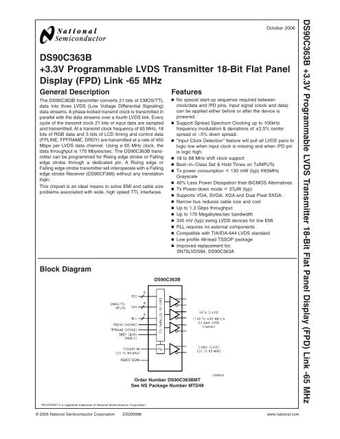
DS90C363B +3.3V Programmable LVDS Transmitter 18 ... - Toradex
DS90C363B +3.3V Programmable LVDS Transmitter 18 ... - Toradex
DS90C363B +3.3V Programmable LVDS Transmitter 18 ... - Toradex

You also want an ePaper? Increase the reach of your titles
YUMPU automatically turns print PDFs into web optimized ePapers that Google loves.
<strong>DS90C363B</strong><br />
<strong>+3.3V</strong> <strong>Programmable</strong> <strong>LVDS</strong> <strong>Transmitter</strong> <strong>18</strong>-Bit Flat Panel<br />
Display (FPD) Link -65 MHz<br />
General Description<br />
The <strong>DS90C363B</strong> transmitter converts 21 bits of CMOS/TTL<br />
data into three <strong>LVDS</strong> (Low Voltage Differential Signaling)<br />
data streams. A phase-locked transmit clock is transmitted in<br />
parallel with the data streams over a fourth <strong>LVDS</strong> link. Every<br />
cycle of the transmit clock 21 bits of input data are sampled<br />
and transmitted. At a transmit clock frequency of 65 MHz, <strong>18</strong><br />
bits of RGB data and 3 bits of LCD timing and control data<br />
(FPLINE, FPFRAME, DRDY) are transmitted at a rate of 455<br />
Mbps per <strong>LVDS</strong> data channel. Using a 65 MHz clock, the<br />
data throughput is 170 Mbytes/sec. The <strong>DS90C363B</strong> transmitter<br />
can be programmed for Rising edge strobe or Falling<br />
edge strobe through a dedicated pin. A Rising edge or<br />
Falling edge strobe transmitter will interoperate with a Falling<br />
edge strobe Receiver (DS90CF366) without any translation<br />
logic.<br />
This chipset is an ideal means to solve EMI and cable size<br />
problems associated with wide, high speed TTL interfaces.<br />
Block Diagram<br />
TRI-STATE ® is a registered trademark of National Semiconductor Corporation.<br />
<strong>DS90C363B</strong><br />
Order Number <strong>DS90C363B</strong>MT<br />
See NS Package Number MTD48<br />
Features<br />
n No special start-up sequence required between<br />
clock/data and /PD pins. Input signal (clock and data)<br />
can be applied either before or after the device is<br />
powered.<br />
n Support Spread Spectrum Clocking up to 100kHz<br />
frequency modulation & deviations of ±2.5% center<br />
spread or −5% down spread.<br />
n "Input Clock Detection" feature will pull all <strong>LVDS</strong> pairs to<br />
logic low when input clock is missing and when /PD pin<br />
is logic high.<br />
n <strong>18</strong> to 68 MHz shift clock support<br />
n Best–in–Class Set & Hold Times on TxINPUTs<br />
n Tx power consumption < 130 mW (typ) @65MHz<br />
Grayscale<br />
n 40% Less Power Dissipation than BiCMOS Alternatives<br />
n Tx Power-down mode < 37µW (typ)<br />
n Supports VGA, SVGA, XGA and Dual Pixel SXGA.<br />
n Narrow bus reduces cable size and cost<br />
n Up to 1.3 Gbps throughput<br />
n Up to 170 Megabytes/sec bandwidth<br />
n 345 mV (typ) swing <strong>LVDS</strong> devices for low EMI<br />
n PLL requires no external components<br />
n Compatible with TIA/EIA-644 <strong>LVDS</strong> standard<br />
n Low profile 48-lead TSSOP package<br />
n Improved replacement for:<br />
SN75<strong>LVDS</strong>84, DS90C363A<br />
20098601<br />
October 2006<br />
<strong>DS90C363B</strong> <strong>+3.3V</strong> <strong>Programmable</strong> <strong>LVDS</strong> <strong>Transmitter</strong> <strong>18</strong>-Bit Flat Panel Display (FPD) Link -65 MHz<br />
© 2006 National Semiconductor Corporation DS200986 www.national.com
<strong>DS90C363B</strong><br />
Absolute Maximum Ratings (Note 1)<br />
If Military/Aerospace specified devices are required,<br />
please contact the National Semiconductor Sales Office/<br />
Distributors for availability and specifications.<br />
Supply Voltage (V CC ) −0.3V to +4V<br />
CMOS/TTL Input Voltage −0.3V to (V CC + 0.3V)<br />
<strong>LVDS</strong> Driver Output Voltage −0.3V to (V CC + 0.3V)<br />
<strong>LVDS</strong> Output Short Circuit<br />
Duration<br />
Continuous<br />
Junction Temperature<br />
+150˚C<br />
Storage Temperature<br />
−65˚C to +150˚C<br />
Lead Temperature<br />
(Soldering, 4 sec)<br />
+260˚C<br />
Maximum Package Power Dissipation Capacity @ 25˚C<br />
MTD48 (TSSOP) Package:<br />
<strong>DS90C363B</strong><br />
1.98 W<br />
Package Derating:<br />
<strong>DS90C363B</strong><br />
ESD Rating<br />
(HBM, 1.5 kΩ, 100 pF)<br />
(EIAJ, 0Ω, 200 pF)<br />
Recommended Operating<br />
Conditions<br />
16 mW/˚C above +25˚C<br />
7 kV<br />
500V<br />
Min Nom Max Units<br />
Supply Voltage (V CC ) 3.0 3.3 3.6 V<br />
Operating Free Air<br />
Temperature (T A ) −10 +25 +70 ˚C<br />
Supply Noise Voltage<br />
(V CC )<br />
200 mV PP<br />
TxCLKIN frequency <strong>18</strong> 68 MHz<br />
Electrical Characteristics<br />
Over recommended operating supply and temperature ranges unless otherwise specified.<br />
Symbol Parameter Conditions Min Typ Max Units<br />
CMOS/TTL DC SPECIFICATIONS<br />
V IH High Level Input Voltage 2.0 V CC V<br />
V IL Low Level Input Voltage GND 0.8 V<br />
V CL Input Clamp Voltage I CL = −<strong>18</strong> mA −0.79 −1.5 V<br />
I IN Input Current V IN = 0.4V, 2.5V or V CC +1.8 +10 µA<br />
V IN = GND −10 0 µA<br />
<strong>LVDS</strong> DC SPECIFICATIONS<br />
V OD Differential Output Voltage R L = 100Ω 250 345 450 mV<br />
∆V OD<br />
Change in V OD between<br />
35 mV<br />
complimentary output states<br />
V OS Offset Voltage (Note 4) 1.13 1.25 1.38 V<br />
∆V OS<br />
Change in V OS between<br />
35 mV<br />
complimentary output states<br />
I OS Output Short Circuit Current V OUT = 0V, R L = 100Ω −3.5 −5 mA<br />
I OZ Output TRI-STATE ® Current Power Down = 0V,<br />
±1 ±10 µA<br />
V OUT =0VorV CC<br />
TRANSMITTER SUPPLY CURRENT<br />
ICCTW<br />
<strong>Transmitter</strong> Supply Current<br />
Worst Case<br />
R L = 100Ω,<br />
C L = 5 pF,<br />
Worst Case Pattern<br />
(Figures 1, 4 ) " Typ "<br />
values are given for V<br />
CC = 3.6V and T A =<br />
+25˚C, " Max " values<br />
are given for V CC =<br />
3.6V and T A = −10˚C<br />
f = 25MHz 29 40 mA<br />
f = 40 MHz 34 45 mA<br />
f = 65 MHz 42 55 mA<br />
www.national.com 2
Electrical Characteristics (Continued)<br />
Over recommended operating supply and temperature ranges unless otherwise specified.<br />
Symbol Parameter Conditions Min Typ Max Units<br />
TRANSMITTER SUPPLY CURRENT<br />
ICCTG <strong>Transmitter</strong> Supply Current<br />
R L = 100Ω,<br />
f = 25 MHz 28 40 mA<br />
16 Grayscale<br />
C L = 5 pF,<br />
16 Grayscale Pattern<br />
(Figures 2, 4 ) " Typ " f = 40 MHz 32 45 mA<br />
values are given for V<br />
CC = 3.6V and T A =<br />
+25˚C, " Max " values<br />
are given for V CC =<br />
3.6V and T A = −10˚C<br />
f = 65 MHz 39 50 mA<br />
ICCTZ<br />
<strong>Transmitter</strong> Supply Current<br />
Power Down<br />
Power Down = Low<br />
Driver Outputs in TRI-STATE ® under<br />
Power Down Mode<br />
11 150 µA<br />
<strong>DS90C363B</strong><br />
Note 1: “Absolute Maximum Ratings” are those values beyond which the safety of the device cannot be guaranteed. They are not meant to imply that the device<br />
should be operated at these limits. The tables of “Electrical Characteristics” specify conditions for device operation.<br />
Note 2: Typical values are given for V CC = 3.3V and T A = +25˚C unless specified otherwise.<br />
Note 3: Current into device pins is defined as positive. Current out of device pins is defined as negative. Voltages are referenced to ground unless otherwise<br />
specified (except V OD and ∆V OD ).<br />
Note 4: V OS previously referred as V CM .<br />
Recommended <strong>Transmitter</strong> Input Characteristics<br />
Over recommended operating supply and temperature ranges unless otherwise specified<br />
Symbol Parameter Min Typ Max Units<br />
TCIT TxCLK IN Transition Time (Figure 5 ) 5 ns<br />
TCIP TxCLK IN Period (Figure 6 ) 14.7 T 50 ns<br />
TCIH TxCLK IN High Time (Figure 6 ) 0.35T 0.5T 0.65T ns<br />
TCIL TxCLK IN Low Time (Figure 6 ) 0.35T 0.5T 0.65T ns<br />
TXIT TxIN, and Power Down pin transition Time 1.5 6.0 ns<br />
TXPD Minimum pulse width for Power Down pin signal 1 us<br />
<strong>Transmitter</strong> Switching Characteristics<br />
Over recommended operating supply and temperature ranges unless otherwise specified<br />
Symbol Parameter Min Typ Max Units<br />
LLHT <strong>LVDS</strong> Low-to-High Transition Time (Figure 4 ) 0.75 1.4 ns<br />
LHLT <strong>LVDS</strong> High-to-Low Transition Time (Figure 4 ) 0.75 1.4 ns<br />
TPPos0 <strong>Transmitter</strong> Output Pulse Position for Bit 0 (Figure 11 ) (Note 5) f = 65 −0.20 0 +0.20 ns<br />
TPPos1 <strong>Transmitter</strong> Output Pulse Position for Bit 1 MHz 2.00 2.20 2.40 ns<br />
TPPos2 <strong>Transmitter</strong> Output Pulse Position for Bit 2 4.20 4.40 4.60 ns<br />
TPPos3 <strong>Transmitter</strong> Output Pulse Position for Bit 3 6.39 6.59 6.79 ns<br />
TPPos4 <strong>Transmitter</strong> Output Pulse Position for Bit 4 8.59 8.79 8.99 ns<br />
TPPos5 <strong>Transmitter</strong> Output Pulse Position for Bit 5 10.79 10.99 11.19 ns<br />
TPPos6 <strong>Transmitter</strong> Output Pulse Position for Bit 6 12.99 13.19 13.39 ns<br />
TPPos0 <strong>Transmitter</strong> Output Pulse Position for Bit 0 (Figure 11 ) (Note 5) f = 40 −0.25 0 +0.25 ns<br />
TPPos1 <strong>Transmitter</strong> Output Pulse Position for Bit 1 MHz 3.32 3.57 3.82 ns<br />
TPPos2 <strong>Transmitter</strong> Output Pulse Position for Bit 2 6.89 7.14 7.39 ns<br />
TPPos3 <strong>Transmitter</strong> Output Pulse Position for Bit 3 10.46 10.71 10.96 ns<br />
TPPos4 <strong>Transmitter</strong> Output Pulse Position for Bit 4 14.04 14.29 14.54 ns<br />
TPPos5 <strong>Transmitter</strong> Output Pulse Position for Bit 5 17.61 17.86 <strong>18</strong>.11 ns<br />
TPPos6 <strong>Transmitter</strong> Output Pulse Position for Bit 6 21.<strong>18</strong> 21.43 21.68 ns<br />
3<br />
www.national.com
<strong>DS90C363B</strong><br />
<strong>Transmitter</strong> Switching Characteristics (Continued)<br />
Over recommended operating supply and temperature ranges unless otherwise specified<br />
Symbol Parameter Min Typ Max Units<br />
TPPos0 <strong>Transmitter</strong> Output Pulse Position for Bit 0 (Figure 11 ) (Note 5) f = 25 −0.45 0 +0.45 ns<br />
TPPos1 <strong>Transmitter</strong> Output Pulse Position for Bit 1 MHz 5.26 5.71 6.16 ns<br />
TPPos2 <strong>Transmitter</strong> Output Pulse Position for Bit 2 10.98 11.43 11.88 ns<br />
TPPos3 <strong>Transmitter</strong> Output Pulse Position for Bit 3 16.69 17.14 17.59 ns<br />
TPPos4 <strong>Transmitter</strong> Output Pulse Position for Bit 4 22.41 22.86 23.31 ns<br />
TPPos5 <strong>Transmitter</strong> Output Pulse Position for Bit 5 28.12 28.57 29.02 ns<br />
TPPos6 <strong>Transmitter</strong> Output Pulse Position for Bit 6 33.84 34.29 34.74 ns<br />
TSTC TxIN Setup to TxCLK IN (Figure 6 ) 2.5 ns<br />
THTC TxIN Hold to TxCLK IN (Figure 6 ) 0.5 ns<br />
TCCD TxCLK IN to TxCLK OUT Delay (Figure 7 ) 50% duty cycle input<br />
clock is assumed, T A = −10˚C, and 65MHz for ” Min ”, T A = 70˚C,<br />
and 25MHz for ” Max ”, V CC = 3.6V, R_FB = V CC<br />
3.340 7.211 ns<br />
SSCG<br />
TxCLK IN to TxCLK OUT Delay (Figure 7 ) 50% duty cycle input<br />
clock is assumed, T A = −10˚C, and 65MHz for ” Min ”, T A = 70˚C,<br />
and 25MHz for ” Max ”, V CC = 3.6V, R_FB = GND<br />
Spread Spectrum Clock support; Modulation frequency with a<br />
linear profile (Note 6)<br />
f=25<br />
MHz<br />
f=40<br />
MHz<br />
f=65<br />
MHz<br />
3.011 6.062 ns<br />
100kHz ±<br />
2.5%/−5%<br />
100kHz ±<br />
2.5%/−5%<br />
100kHz ±<br />
2.5%/−5%<br />
TPLLS <strong>Transmitter</strong> Phase Lock Loop Set (Figure 8 ) 10 ms<br />
TPDD <strong>Transmitter</strong> Power Down Delay (Figure 10 ) 100 ns<br />
Note 5: The Minimum and Maximum Limits are based on statistical analysis of the device performance over process, voltage, and temperature ranges. This<br />
parameter is functionality tested only on Automatic Test Equipment (ATE).<br />
Note 6: Care must be taken to ensure TSTC and THTC are met so input data are sampling correctly. This SSCG parameter only shows the performance of tracking<br />
Spread Spectrum Clock applied to TxCLK IN pin, and reflects the result on TxCLKOUT+ and TxCLK− pins.<br />
AC Timing Diagrams<br />
20098604<br />
FIGURE 1. “Worst Case” Test Pattern<br />
www.national.com 4
AC Timing Diagrams (Continued)<br />
<strong>DS90C363B</strong><br />
20098605<br />
FIGURE 2. “16 Grayscale” Test Pattern (Notes 7, 8, 9, 10)<br />
Note 7: The worst case test pattern produces a maximum toggling of digital circuits, <strong>LVDS</strong> I/O and CMOS/TTL I/O.<br />
Note 8: The 16 grayscale test pattern tests device power consumption for a “typical” LCD display pattern. The test pattern approximates signal switching needed<br />
to produce groups of 16 vertical stripes across the display.<br />
Note 9: Figures 1, 2 show a falling edge data strobe (TxCLK IN/RxCLK OUT).<br />
Note 10: Recommended pin to signal mapping. Customer may choose to define differently.<br />
20098630<br />
FIGURE 3. <strong>DS90C363B</strong> (<strong>Transmitter</strong>) <strong>LVDS</strong> Output Load<br />
20098606<br />
FIGURE 4. <strong>DS90C363B</strong> (<strong>Transmitter</strong>) <strong>LVDS</strong> Transition Times<br />
5<br />
www.national.com
<strong>DS90C363B</strong><br />
AC Timing Diagrams (Continued)<br />
20098608<br />
FIGURE 5. <strong>DS90C363B</strong> (<strong>Transmitter</strong>) Input Clock Transition Time<br />
20098610<br />
FIGURE 6. <strong>DS90C363B</strong> (<strong>Transmitter</strong>) Setup/Hold and High/Low Times (Falling Edge Strobe)<br />
20098612<br />
FIGURE 7. <strong>DS90C363B</strong> (<strong>Transmitter</strong>) Clock In to Clock Out Delay (Falling Edge Strobe)<br />
20098614<br />
FIGURE 8. <strong>DS90C363B</strong> (<strong>Transmitter</strong>) Phase Lock Loop Set Time<br />
www.national.com 6
AC Timing Diagrams (Continued)<br />
<strong>DS90C363B</strong><br />
20098617<br />
FIGURE 9. 21 Parallel TTL Data Inputs Mapped to <strong>LVDS</strong> Outputs<br />
200986<strong>18</strong><br />
FIGURE 10. <strong>Transmitter</strong> Power Down Delay<br />
7<br />
www.national.com
<strong>DS90C363B</strong><br />
AC Timing Diagrams (Continued)<br />
20098626<br />
FIGURE 11. <strong>Transmitter</strong> <strong>LVDS</strong> Output Pulse Position Measurement<br />
<strong>DS90C363B</strong> Pin Descriptions — FPD Link <strong>Transmitter</strong><br />
Pin Name I/O No. Description<br />
TxIN I 21 TTL level input. This includes: 6 Red, 6 Green, 6 Blue, and 3 control lines — FPLINE,<br />
FPFRAME and DRDY (also referred to as HSYNC, VSYNC, Data Enable).<br />
TxOUT+ O 3 Positive <strong>LVDS</strong> differentiaI data output.<br />
TxOUT− O 3 Negative <strong>LVDS</strong> differential data output.<br />
FPSHIFT IN I 1 TTL Ievel clock input. The falling edge acts as data strobe. Pin name TxCLK IN.<br />
R_FB I 1 <strong>Programmable</strong> strobe select (See Table 1).<br />
TxCLK OUT+ O 1 Positive <strong>LVDS</strong> differential clock output.<br />
TxCLK OUT− O 1 Negative <strong>LVDS</strong> differential clock output.<br />
PWR DOWN I 1 TTL level input. Assertion (low input) TRI-STATES the outputs, ensuring low current at power<br />
down. See Applications Information section.<br />
V CC I 3 Power supply pins for TTL inputs.<br />
GND I 4 Ground pins for TTL inputs.<br />
PLL V CC I 1 Power supply pin for PLL.<br />
PLL GND I 2 Ground pins for PLL.<br />
<strong>LVDS</strong> V CC I 1 Power supply pin for <strong>LVDS</strong> outputs.<br />
<strong>LVDS</strong> GND I 3 Ground pins for <strong>LVDS</strong> outputs.<br />
NC 1 No connect<br />
www.national.com 8
Applications Information<br />
The <strong>DS90C363B</strong> are backward compatible with the<br />
DS90C363/DS90CF363, DS90C363A/DS90CF363A and<br />
are a pin-for-pin replacement.<br />
This device may also be used as a replacement for the<br />
DS90CF563 (5V, 65MHz) and DS90CF561 (5V, 40MHz)<br />
FPD-Link <strong>Transmitter</strong>s with certain considerations/<br />
modifications:<br />
1. Change 5V power supply to 3.3V. Provide this supply to<br />
the V CC , <strong>LVDS</strong> V CC and PLL V CC of the transmitter.<br />
2. To implement a falling edge device for the <strong>DS90C363B</strong>,<br />
the R_FB pin (pin 14) may be tied to ground OR left<br />
unconnected (an internal pull-down resistor biases this<br />
pin low). Biasing this pin to Vcc implements a rising edge<br />
device.<br />
TRANSMITTER INPUT PINS<br />
The <strong>DS90C363B</strong> transmitter input and control inputs accept<br />
3.3V LVTTL/LVCMOS levels. They are not 5V tolerant.<br />
TRANSMITTER INPUT CLOCK/DATA SEQUENCING<br />
The <strong>DS90C363B</strong> does not require any special requirement<br />
for sequencing of the input clock/data and PD (PowerDown)<br />
signal. The <strong>DS90C363B</strong> offers a more robust input sequencing<br />
feature where the input clock/data can be inserted after<br />
the release of the PD signal. In the case where the clock/<br />
data is stopped and reapplied, such as changing video mode<br />
within Graphics Controller, it is not necessary to cycle the PD<br />
Pin Diagram<br />
signal. However, there are in certain cases where the PD<br />
may need to be asserted during these mode changes. In<br />
cases where the source (Graphics Source) may be supplying<br />
an unstable clock or spurious noisy clock output to the<br />
<strong>LVDS</strong> transmitter, the <strong>LVDS</strong> <strong>Transmitter</strong> may attempt to lock<br />
onto this unstable clock signal but is unable to do so due the<br />
instability or quality of the clock source. The PD signal in<br />
these cases should then be asserted once a stable clock is<br />
applied to the <strong>LVDS</strong> transmitter. Asserting the PWR DOWN<br />
pin will effectively place the device in reset and disable the<br />
PLL, enabling the <strong>LVDS</strong> <strong>Transmitter</strong> into a power saving<br />
standby mode. However, it is still generally a good practice<br />
to assert the PWR DOWN pin or reset the <strong>LVDS</strong> transmitter<br />
whenever the clock/data is stopped and reapplied but it is<br />
not mandatory for the <strong>DS90C363B</strong>.<br />
SPREAD SPECTRUM CLOCK SUPPORT<br />
The <strong>DS90C363B</strong> can support Spread Spectrum Clocking<br />
signal type inputs. The DS90C383B outputs will accurately<br />
track Spread Spectrum Clock/Data inputs with modulation<br />
frequencies of up to 100kHz (max.)with either center spread<br />
of ±2.5% or down spread -5% deviations.<br />
POWER SOURCES SEQUENCE<br />
In typical applications, it is recommended to have V CC , <strong>LVDS</strong><br />
V CC and PLL V CC from the same power source with three<br />
separate de-coupling bypass capacitor groups. There is no<br />
requirement on which VCC entering the device first.<br />
<strong>DS90C363B</strong><br />
<strong>DS90C363B</strong><br />
20098623<br />
9<br />
www.national.com
<strong>DS90C363B</strong><br />
Typical Application<br />
20098603<br />
TABLE 1. <strong>Programmable</strong> <strong>Transmitter</strong> (<strong>DS90C363B</strong>)<br />
Pin Condition Strobe Status<br />
R_FB R_FB = V CC Rising edge strobe<br />
R_FB R_FB = GND or NC Falling edge strobe<br />
www.national.com 10
Physical Dimensions inches (millimeters) unless otherwise noted<br />
<strong>DS90C363B</strong><br />
48-Lead Molded Thin Shrink Small Outline Package, JEDEC<br />
Order Number <strong>DS90C363B</strong>MT<br />
NS Package Number MTD48<br />
11<br />
www.national.com
<strong>DS90C363B</strong> <strong>+3.3V</strong> <strong>Programmable</strong> <strong>LVDS</strong> <strong>Transmitter</strong> <strong>18</strong>-Bit Flat Panel Display (FPD) Link -65 MHz<br />
National does not assume any responsibility for use of any circuitry described, no circuit patent licenses are implied and National reserves<br />
the right at any time without notice to change said circuitry and specifications.<br />
For the most current product information visit us at www.national.com.<br />
LIFE SUPPORT POLICY<br />
NATIONAL’S PRODUCTS ARE NOT AUTHORIZED FOR USE AS CRITICAL COMPONENTS IN LIFE SUPPORT DEVICES OR SYSTEMS<br />
WITHOUT THE EXPRESS WRITTEN APPROVAL OF THE PRESIDENT AND GENERAL COUNSEL OF NATIONAL SEMICONDUCTOR<br />
CORPORATION. As used herein:<br />
1. Life support devices or systems are devices or systems<br />
which, (a) are intended for surgical implant into the body, or<br />
(b) support or sustain life, and whose failure to perform when<br />
properly used in accordance with instructions for use<br />
provided in the labeling, can be reasonably expected to result<br />
in a significant injury to the user.<br />
2. A critical component is any component of a life support<br />
device or system whose failure to perform can be reasonably<br />
expected to cause the failure of the life support device or<br />
system, or to affect its safety or effectiveness.<br />
BANNED SUBSTANCE COMPLIANCE<br />
National Semiconductor follows the provisions of the Product Stewardship Guide for Customers (CSP-9-111C2) and Banned Substances<br />
and Materials of Interest Specification (CSP-9-111S2) for regulatory environmental compliance. Details may be found at:<br />
www.national.com/quality/green.<br />
Lead free products are RoHS compliant.<br />
National Semiconductor<br />
Americas Customer<br />
Support Center<br />
Email: new.feedback@nsc.com<br />
Tel: 1-800-272-9959<br />
www.national.com<br />
National Semiconductor<br />
Europe Customer Support Center<br />
Fax: +49 (0) <strong>18</strong>0-530 85 86<br />
Email: europe.support@nsc.com<br />
Deutsch Tel: +49 (0) 69 9508 6208<br />
English Tel: +44 (0) 870 24 0 2171<br />
Français Tel: +33 (0) 1 41 91 8790<br />
National Semiconductor<br />
Asia Pacific Customer<br />
Support Center<br />
Email: ap.support@nsc.com<br />
National Semiconductor<br />
Japan Customer Support Center<br />
Fax: 81-3-5639-7507<br />
Email: jpn.feedback@nsc.com<br />
Tel: 81-3-5639-7560