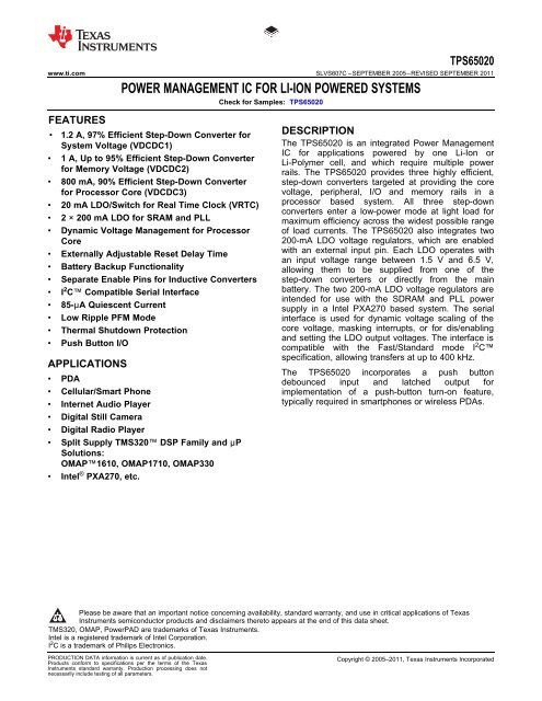
Texas Instruments TPS65020 Power Management IC - Toradex
Texas Instruments TPS65020 Power Management IC - Toradex
Texas Instruments TPS65020 Power Management IC - Toradex
You also want an ePaper? Increase the reach of your titles
YUMPU automatically turns print PDFs into web optimized ePapers that Google loves.
<strong>TPS65020</strong>SLVS607C –SEPTEMBER 2005–REVISED SEPTEMBER 2011www.ti.comELECTR<strong>IC</strong>AL CHARACTERIST<strong>IC</strong>S (continued)VINDCDC1 = VINDCDC2 = VINDCDC3 = VCC = VINLDO = 3.6 V, VBACKUP = 3 V, T A = –40°C to 85°C, typical values areat T A = 25°C (unless otherwise noted)PARAMETER TEST CONDITIONS MIN TYP MAX UNITResetpwron threshold VRTC falling –3% 2.4 3% VResetpwron threshold VRTC rising –3% 2.52 3% VI LK leakage current output inactive high 0.1 μA4 Submit Documentation Feedback Copyright © 2005–2011, <strong>Texas</strong> <strong>Instruments</strong> IncorporatedProduct Folder Link(s) : <strong>TPS65020</strong>
<strong>TPS65020</strong>SLVS607C –SEPTEMBER 2005–REVISED SEPTEMBER 2011www.ti.comELECTR<strong>IC</strong>AL CHARACTERIST<strong>IC</strong>SVINDCDC1 = VINDCDC2 = VINDCDC3 = VCC = VINLDO = 3.6 V, VBACKUP = 3 V, T A = –40°C to 85°C, typical values areat T A = 25°C (unless otherwise noted)PARAMETER TEST CONDITIONS MIN TYP MAX UNITSUPPLY PINS: VBACKUP, VSYSIN, VRTCVBACKUP = 3 V, VSYSIN = 0 V;I (q) Operating quiescent current 20 33 μAVCC = 2.6 V, current into VBACKUPVBACKUP < V_VBACKUP, current intoI (SD) Operating quiescent current 2 3 μAVBACKUPVRTC LDO output voltage VSYSIN = VBACKUP = 0 V, I O = 0 mA 3 VI O Output current for VRTC VSYSIN < 2.57 V and VBACKUP < 2.57 V 20 mAVRTC short-circuit current limit VRTC = GND; VSYSIN = VBACKUP = 0 V 100 mAMaximum output current at VRTC for VRTC > 2.6 V, V CC = 3 V;RESPWRON = 1VSYSIN = VBACKUP = 0 V30 mAV O Output voltage accuracy for VRTC VSYSIN = VBACKUP = 0 V; I O = 0 mA ±1%Line regulation for VRTC VCC = VRTC + 0.5 V to 6.5 V, I O = 5 mA ±1%I O = 1 mA to 20 mA;Load regulation VRTC ±2%VSYSIN = VBACKUP = 0 VRegulation time for VRTC Load change from 10% to 90% 10 μsI lkg Input leakage current at VSYSIN VSYSIN < V_VSYSIN 2 μASUPPLY PIN: VINLDOr DS(on) of VSYSIN switch 12.5 Ωr DS(on) of VBACKUP switch 12.5 ΩInput voltage range at VBACKUP (1) 2.73 3.75 VInput voltage range at VSYSIN (1) 2.73 3.75 VVSYSIN threshold VSYSIN falling –3% 2.55 3% VVSYSIN threshold VSYSIN rising –3% 2.65 3% VVBACKUP threshold VBACKUP falling –3% 2.55 3% VVBACKUP threshold VBACKUP falling -3% 2.65 3% VI (q) Operating quiescent current Current per LDO into VINLDO 16 30 μATotal current for both LDOs into VINLDO,I (SD) Shutdown current 0.1 1 μAVLDO = 0 V(1) Based on the requirements for the Intel PXA270 processor.6 Submit Documentation Feedback Copyright © 2005–2011, <strong>Texas</strong> <strong>Instruments</strong> IncorporatedProduct Folder Link(s) : <strong>TPS65020</strong>
<strong>TPS65020</strong>www.ti.com SLVS607C –SEPTEMBER 2005–REVISED SEPTEMBER 2011ELECTR<strong>IC</strong>AL CHARACTERIST<strong>IC</strong>SVINDCDC1 = VINDCDC2 = VINDCDC3 = VCC = VINLDO = 3.6 V, VBACKUP = 3 V, T A = –40°C to 85°C, typical values areat T A = 25°C (unless otherwise noted)VDCDC1 STEP-DOWN CONVERTERPARAMETER TEST CONDITIONS MIN TYP MAX UNITV I Input voltage range, VINDCDC1 2.5 6 VI O Maximum output current 1200 mAI (SD) Shutdown supply current in VINDCDC1 DCDC1_EN = GND 0.1 1 μAr DS(on) P-channel MOSFET on-resistance VINDCDC1 = V (GS) = 3.6 V 125 261 mΩI lkg P-channel leakage current VINDCDC1 = 6 V 2 μAr DS(on) N-channel MOSFET on-resistance VINDCDC1 = V (GS) = 3.6 V 130 260 mΩI lkg N-channel leakage current V (DS) = 6 V 7 10 μAForward current limit (P- and N-channel) 2.5 V < V I(MAIN) < 6 V 1.55 1.75 1.95 Af S Oscillator frequency 1.3 1.5 1.7 MHzVINDCDC1 = 3.3 V to 6 V;3 VFixed output voltage0 mA ≤ I O ≤ 1.2 A–2% 2%FPWMDCDC1=0 VINDCDC1 = 3.6 V to 6 V;3.3 V0 mA ≤ I O ≤ 1.2 A–2% 2%VINDCDC1 = 3.3 V to 6 V;3 VFixed output voltage0 mA ≤ I O ≤ 1.2 A–1% 1%FPWMDCDC1=1 VINDCDC1 = 3.6 V to 6 V;3.3 V0 mA ≤ I O ≤ 1.2 A–1% 1%Adjustable output voltage with resistor VINDCDC1 = VDCDC1 +0.3 V (min 2.5 V)divider at DEFDCDC1 FPWMDCDC1=0 to 6 V; 0 mA ≤ I O ≤ 1.2 AAdjustable output voltage with resistor VINDCDC1 = VDCDC1 +0.3 V (min 2.5 V)divider at DEFDCDC1; FPWMDCDC1=1 to 6 V; 0 mA ≤ I O ≤ 1.2 A–2% 2%–1% 1%VINDCDC1 = VDCDC1 + 0.3 V (min. 2.5 V)Line Regulation 0 %/Vto 6 V; I O = 10 mALoad Regulation I O = 10 mA to 1200 mA 0.25 %/AVDCDC1 ramping from 5% to 95% of targetSoft start ramp time 750 μsvalueInternal resistance from L1 to GND 1 MΩVDCDC1 discharge resistance 300 ΩCopyright © 2005–2011, <strong>Texas</strong> <strong>Instruments</strong> Incorporated Submit Documentation Feedback 7Product Folder Link(s) : <strong>TPS65020</strong>
<strong>TPS65020</strong>SLVS607C –SEPTEMBER 2005–REVISED SEPTEMBER 2011www.ti.comELECTR<strong>IC</strong>AL CHARACTERIST<strong>IC</strong>SVINDCDC1 = VINDCDC2 = VINDCDC3 = VCC = VINLDO = 3.6 V, VBACKUP = 3 V, T A = –40°C to 85°C, typical values areat T A = 25°C (unless otherwise noted)VDCDC2 STEP-DOWN CONVERTERPARAMETER TEST CONDITIONS MIN TYP MAX UNITV I Input voltage range, VINDCDC2 2.5 6 VI O Maximum output current 1000 mAI (SD) Shutdown supply current in VINDCDC2 DCDC2_EN = GND 0.1 1 μAr DS(on) P-channel MOSFET on-resistance VINDCDC2 = V (GS) = 3.6 V 140 300 mΩI lkg P-channel leakage current VINDCDC2 = 6 V 2 μAr DS(on) N-channel MOSFET on-resistance VINDCDC2 = V (GS) = 3.6 V 150 297 mΩI lkg N-channel leakage current V (DS) = 6 V 7 10 μAI LIMF Forward current limit (P- and N-channel) 2.5 V < VINDCDC2 < 6 V 1.4 1.55 1.7 Af S Oscillator frequency 1.3 1.5 1.7 MHzVINDCDC2 = 2.5 V to 6 V;1.8 VFixed output voltage0 mA ≤ I O ≤ 1 A–2% 2%FPWMDCDC2=0 VINDCDC2 = 2.8 V to 6 V;2.5 V0 mA ≤ I O ≤ 1 A–2% 2%VINDCDC2 = 2.5 V to 6 V;1.8 VFixed output voltage0 mA ≤ I O ≤ 1 A–2% 2%FPWMDCDC2=1 VINDCDC2 = 2.8 V to 6 V;2.5 V0 mA ≤ I O ≤ 1 A–1% 1%Adjustable output voltage with resistor VINDCDC2 = VDCDC2 +0.3 V (min 2.5 V)divider at DEFDCDC2 FPWMDCDC2=0 to 6 V; 0 mA ≤ I O ≤ 1 AAdjustable output voltage with resistor VINDCDC2 = VDCDC2 +0.3 V (min 2.5 V)divider at DEFDCDC2; FPWMDCDC2=1 to 6 V; 0 mA ≤ I O ≤ 1 A–2% 2%–1% 1%VINDCDC2 = VDCDC2 + 0.3 V (min. 2.5 V)Line Regulation 0 %/Vto 6 V; I O = 10 mALoad Regulation I O = 10 mA to 1 mA 0.25 %/AVDCDC2 ramping from 5% to 95% of targetSoft start ramp time 750 μsvalueInternal resistance from L2 to GND 1 MΩVDCDC2 discharge resistance 300 Ω8 Submit Documentation Feedback Copyright © 2005–2011, <strong>Texas</strong> <strong>Instruments</strong> IncorporatedProduct Folder Link(s) : <strong>TPS65020</strong>
<strong>TPS65020</strong>www.ti.com SLVS607C –SEPTEMBER 2005–REVISED SEPTEMBER 2011ELECTR<strong>IC</strong>AL CHARACTERIST<strong>IC</strong>SVINDCDC1 = VINDCDC2 = VINDCDC3 = VCC = VINLDO = 3.6 V, VBACKUP = 3 V, T A = –40°C to 85°C, typical values areat T A = 25°C (unless otherwise noted)VDCDC3 STEP-DOWN CONVERTERPARAMETER TEST CONDITIONS MIN TYP MAX UNITV I Input voltage range, VINDCDC3 2.5 6 VI O Maximum output current 800 mAI (SD) Shutdown supply current in VINDCDC3 DCDC3_EN = GND 0.1 1 μAr DS(on) P-channel MOSFET on-resistance VINDCDC3 = V (GS) = 3.6 V 310 698 mΩI lkg P-channel leakage current VINDCDC3 = 6 V 0.1 2 μAr DS(on) N-channel MOSFET on-resistance VINDCDC3 = V (GS) = 3.6 V 220 503 mΩI lkg N-channel leakage current V (DS) = 6 V 7 10 μAForward current limit (P- and N-channel) 2.5 V < VINDCDC3 < 6 V 1.05 1.2 1.35 Af S Oscillator frequency 1.3 1.5 1.7 MHzFixed output voltage VINDCDC3 = 2.5 V to 6 V;FPWMDCDC3=0 0 mA ≤ I O ≤ 600 mAAll VDCDC3Fixed output voltage VINDCDC3 = 2.5 V to 6 V;FPWMDCDC3=1 0 mA ≤ I O ≤ 600 mAAdjustable output voltage with resistor VINDCDC3 = VDCDC3 +0.4 V (min 2.5 V) todivider at DEFDCDC3 FPWMDCDC3=0 6 V; 0 mA ≤ I O ≤ 600 mAAdjustable output voltage with resistor VINDCDC3 = VDCDC3 +0.4 V (min 2.5 V) todivider at DEFDCDC3; FPWMDCDC3=1 6 V; 0 mA ≤ I O ≤ 600 mA–2% 2%–1% 1%–2% 2%–1% 1%VINDCDC3 = VDCDC3 + 0.3 V (min. 2.5 V)Line Regulation 0 %/Vto 6 V; I O = 10 mALoad Regulation I O = 10 mA to 400 mA 0.25 %/AVDCDC3 ramping from 5% to 95% of targetSoft start ramp time 750 μsvalueInternal resistance from L3 to GND 1 MΩVDCDC3 discharge resistance 300 ΩCopyright © 2005–2011, <strong>Texas</strong> <strong>Instruments</strong> Incorporated Submit Documentation Feedback 9Product Folder Link(s) : <strong>TPS65020</strong>
<strong>TPS65020</strong>SLVS607C –SEPTEMBER 2005–REVISED SEPTEMBER 2011www.ti.comELECTR<strong>IC</strong>AL CHARACTERIST<strong>IC</strong>SVINDCDC1 = VINDCDC2 = VINDCDC3 = VCC = VINLDO = 3.6 V, VBACKUP = 3 V, T A = –40°C to 85°C, typical values areat T A = 25°C (unless otherwise noted)PARAMETER TEST CONDITIONS MIN TYP MAX UNITVLDO1 and VLDO2 LOW DROPOUT REGULATORSV I Input voltage range for LDO1, 2 1.5 6.5 VV O LDO1 output voltage range 1 3.3 VV O LDO2 output voltage range 1 3.3 VMaximum output current for LDO1,I O 200 mALDO2LDO1 and LDO2 short-circuitI (SC) VLDO1 = GND, VLDO2 = GND 400 mAcurrent limitMinimum voltage drop at LDO1,LDO2Output voltage accuracy for LDO1,LDO2I O = 50 mA, VINLDO = 1.8 V 120I O = 50 mA, VINLDO = 1.5 V 65 150 mVI O = 200 mA, VINLDO = 1.8 V 300I O = 10 mA –2% 1%VINLDO1,2 = VLDO1, 2 + 0.5 VLine regulation for LDO1, LDO2 –1% 1%(min. 2.5 V) to 6.5 V, I O = 10 mALoad regulation for LDO1, LDO2 I O = 0 mA to 50 mA –1% 1%Regulation time for LDO1, LDO2 Load change from 10% to 90% 10 μsANALOG<strong>IC</strong> SIGNALS DEFDCDC1, DEFDCDC2, DEFDCDC3V IH High level input voltage 1.3 VCC VV IL Low level input voltage 0 0.1 VI H Input bias current 0.001 0.05 μALOG<strong>IC</strong> SIGNALS PB_IN; PB_OUTV OL Low level output voltage at PB_OUT I OL = 20 mA 0.5 VV OH High level output voltage PB_OUT 6 VV IL Low level input voltage PB_IN 0.4 VV IH High level input voltage PB_IN 1.3 V CC(1) VTHERMAL SHUTDOWNII Input leakage current PB_IN 1 μAT (SD) Thermal shutdown Increasing junction temperature 160 °CThermal shutdown hysteresis Decreasing junction temperature 20 °CINTERNAL UNDERVOLTAGE LOCK OUTUVLO Internal UVLO VCC falling –2% 2.35 2% VV (UVLO_HYST) Internal UVLO comparator hysteresis 120 mVVOLTAGE DETECTOR COMPARATORSPOWER GOODComparator threshold(PWRFAIL_SNS, LOWBAT_SNS)Falling threshold –1% 1.0 1% VHysteresis 40 50 60 mVPropagation delay 25 mV overdrive 10 μsVDCDC1, VDCDC2, VDCDC3, VLDO1,V (PGOODF) –12% –10% –8%VLDO2, decreasingVDCDC1, VDCDC2, VDCDC3, VLDO1,V (PGOODR) –7% –5% –3%VLDO2, increasing(1) The input voltage can go as high as 6 V. If the input voltage exceeds VCC, an input current of (V (PB_IN) - 0.7 V - VCC) / 10 kΩ flows.10 Submit Documentation Feedback Copyright © 2005–2011, <strong>Texas</strong> <strong>Instruments</strong> IncorporatedProduct Folder Link(s) : <strong>TPS65020</strong>
<strong>TPS65020</strong>www.ti.com SLVS607C –SEPTEMBER 2005–REVISED SEPTEMBER 2011PIN ASSIGNMENT(TOP VIEW)AGND1LOWBAT_SNSPWRFAIL_SNSVCCVINDCDC2L2PGND2VDCDC2DEFDCDC2PWRFAILDEFDCDC3VDCDC3PGND3L3VINDCDC3VINDCDC1L1PGND1VDCDC1DEFDCDC140 39 38 37 36 35 34 33 32 31130229328427526625724823922102111 12 13 14 15 16 17 18 19 20SCLKSDATINTRESPWRONTRESPWRONDCDC1_ENDCDC2_ENDCDC3_ENLDO_ENLOWBATHOT_RESETPB_INPB_OUTVSYSINVBACKUPVRTCAGND2VLDO2VINLDOVLDO1TERMINAL FUNCTIONSTERMINALNAMENO.I/ODESCRIPTIONSWITCHING REGULATOR SECTIONAGND1 40 Analog ground connection. All analog ground pins are connected internally on the chip.AGND2 17 Analog ground connection. All analog ground pins are connected internally on the chip.<strong>Power</strong>PAD – Connect the power pad to analog ground.VINDCDC1 6 IInput voltage for VDCDC1 step-down converter. This must be connected to the same voltage supplyas VINDCDC2, VINDCDC3, and VCC.L1 7 Switch pin of VDCDC1 converter. The VDCDC1 inductor is connected here.VDCDC1 9 I VDCDC1 feedback voltage sense input, connect directly to VDCDC1PGND1 8 <strong>Power</strong> ground for VDCDC1 converterVINDCDC2 36 IInput voltage for VDCDC2 step-down converter. This must be connected to the same voltage supplyas VINDCDC1, VINDCDC3, and VCC.L2 35 Switch pin of VDCDC2 converter. The VDCDC2 inductor is connected here.VDCDC2 33 I VDCDC2 feedback voltage sense input, connect directly to VDCDC2PGND2 34 <strong>Power</strong> ground for VDCDC2 converterVINDCDC3 5 IInput voltage for VDCDC3 step-down converter. This must be connected to the same voltage supplyas VINDCDC1, VINDCDC2, and VCC.L3 4 Switch pin of VDCDC3 converter. The VDCDC3 inductor is connected here.VDCDC3 2 I VDCDC3 feedback voltage sense input, connect directly to VDCDC3PGND3 3 <strong>Power</strong> ground for VDCDC3 converterCopyright © 2005–2011, <strong>Texas</strong> <strong>Instruments</strong> Incorporated Submit Documentation Feedback 11Product Folder Link(s) : <strong>TPS65020</strong>
<strong>TPS65020</strong>SLVS607C –SEPTEMBER 2005–REVISED SEPTEMBER 2011www.ti.comNAMETERMINALNO.I/OTERMINAL FUNCTIONS (continued)DESCRIPTION<strong>Power</strong> supply for digital and analog circuitry of VDCDC1, VDCDC2, and VDCDC3 dc-dc converters.VCC 37 I This must be connected to the same voltage supply as VINDCDC3, VINDCDC1, and VINDCDC2.Also supplies serial interface blockInput signal indicating default VDCDC1 voltage, 0 = 3 V, 1 = 3.3 V This pin can also be connected toDEFDCDC1 10 I a resistor divider between VDCDC1 and GND. If the output voltage of the DCDC1 converter is set ina range from 0.6 V to VINDCDC1 VInput signal indicating default VDCDC2 voltage, 0 = 1.8 V, 1 = 2.5 V This pin can also be connectedDEFDCDC2 32 I to a resistor divider between VDCDC2 and GND. If the output voltage of the DCDC2 converter is setin a range from 0.6 V to VINDCDC2 VInput signal indicating default VDCDC3 voltage, 0 = 1.3 V, 1 = 1.55 V This pin can also be connectedDEFDCDC3 1 I to a resistor divider between VDCDC3 and GND. If the output voltage of the DCDC3 converter is setin a range from 0.6 V to VINDCDC3 VDCDC1_EN 25 I VDCDC1 enable pin. A logic high enables the regulator, a logic low disables the regulator.DCDC2_EN 24 I VDCDC2 enable pin. A logic high enables the regulator, a logic low disables the regulator.DCDC3_EN 23 I VDCDC3 enable pin. A logic high enables the regulator, a logic low disables the regulator.LDO REGULATOR SECTIONVINLDO 19 I I Input voltage for LDO1 and LDO2VLDO1 20 O Output voltage of LDO1VLDO2 18 O Output voltage of LDO2LDO_EN 22 I Enable input for LDO1 and LDO2. Logic high enables the LDOs, logic low disables the LDOsVBACKUP 15 I Connect the backup battery to this input pin.VRTC 16 O Output voltage of the LDO/switch for the real time clockVSYSIN 14 I Input of system voltage for VRTC switchCONTROL AND I 2 C SECTIONHOT_RESET 11 I Push button input used to reboot or wake-up processor via RESPWRON output pinTRESPWRON 26 I Connect the timing capacitor to this pin to set the reset delay time: 1 nF → 100 msRESPWRON 27 O Open drain System reset outputPWRFAIL 31 O Open drain output. Active low when PWRFAIL comparator indicates low VBAT condition.LOW_BAT 21 O Open drain output of LOW_BAT comparatorINT 28 O Open drain outputSCLK 30 I Serial interface clock lineSDAT 29 I/O Serial interface data/addressPWRFAIL_SNS 38 I Input for the comparator driving the PWRFAIL outputLOWBAT_SNS 39 I Input for the comparator driving the LOW_BAT outputPB_IN 12 I/O Push button input debounced and output fed to latch at PB_OUTPB_OUT 13 I/O Open drain output of latch driven by PB_IN. Low after power up.12 Submit Documentation Feedback Copyright © 2005–2011, <strong>Texas</strong> <strong>Instruments</strong> IncorporatedProduct Folder Link(s) : <strong>TPS65020</strong>
<strong>TPS65020</strong>www.ti.com SLVS607C –SEPTEMBER 2005–REVISED SEPTEMBER 2011FUNCTIONAL BLOCK DIAGRAMVSYSINVCCTHERMALSHUTDOWNVBACKUPVRTCBBATSWITCHVINDCDC1SCLKSDATSerial InterfaceDCDC1STEP-DOWNCONVER TERL1VDCDC1DEFDCDC1PGND1DCDC1_ENDCDC2_ENDCDC3_ENLDO_ENHOT_RESETCONTROLDCDC2STEP-DOWNCONVERTERVINDCDC2L2VDCDC2DEFDCDC2PGND2RESPWRONVCCINTAGND1VINDCDC3LOWBAT_SNSPWRFAIL_SNSLOW_BATTPWRFAILTRESPWRONUVLOVREFOSCDCDC3STEP-DOWNCONVERTERL3VDCDC3DEFDCDC3PGND3PB_INInput bufferJK-flipflopVLDO1VLDO1PB_OUT200-mA LDOAGND2VINLDOVLDO2200-mA LDOVLDO2Copyright © 2005–2011, <strong>Texas</strong> <strong>Instruments</strong> Incorporated Submit Documentation Feedback 13Product Folder Link(s) : <strong>TPS65020</strong>
<strong>TPS65020</strong>SLVS607C –SEPTEMBER 2005–REVISED SEPTEMBER 2011www.ti.comTYP<strong>IC</strong>AL CHARACTERIST<strong>IC</strong>SGraphs were taken using the EVM with the following inductor/output capacitor combinations:CONVERTER INDUCTOR OUTPUT CAPACITOR OUTPUT CAPACITOR VALUEVDCDC1 VLCF4020-2R2 C2012X5R0J106M 2 × 10 μFVDCDC2 VLCF4020-2R2 C2012X5R0J106M 2 × 10 μFVDCDC3 VLF4012AT-2R2M1R5 C2012X5R0J106M 2 × 10 μFTable 1. Table of GraphsFIGUREη Efficiency vs Output current 1, 2, 3, 4, 5, 6, 7Line transient response 8, 9, 10Load transient response 11, 12, 13VDCDC2 PFM operation 14VDCDC2 low ripple PFM operation 15VDCDC2 PWM operation 16Startup VDCDC1, VDCDC2 and VDCDC3 17Startup LDO1 and LDO2 18Line transient response 19, 20, 21Load transient response 22, 23, 24DCDC1: EFF<strong>IC</strong>IENCYvsOUTPUT CURRENTDCDC1: EFF<strong>IC</strong>IENCYvsOUTPUT CURRENTV = 3.8 V IV = 5 V IV = 4.2 V IV = 4.2 V IEfficiency - %Efficiency - %V = 3.8 V IV = 5 V IoT A = 25 CV O = 3.3 VPFM / PWM ModeoT A = 25 CV O = 3.3 VPWM Mode0.01 0.1 1 10 100 1 k 10 k0.01 0.1 1 10 100 1 k 10 kIO- Output Current - mAIO- Output Current - mAFigure 1. Figure 2.14 Submit Documentation Feedback Copyright © 2005–2011, <strong>Texas</strong> <strong>Instruments</strong> IncorporatedProduct Folder Link(s) : <strong>TPS65020</strong>
<strong>TPS65020</strong>www.ti.com SLVS607C –SEPTEMBER 2005–REVISED SEPTEMBER 2011DCDC2: EFF<strong>IC</strong>IENCYvsOUTPUT CURRENTDCDC2: EFF<strong>IC</strong>IENCYvsOUTPUT CURRENTV = 2.5 V IEfficiency - %V = 4.2 V IV = 5 V IV = 3.8 V IEfficiency - %V = 3.8 V IV = 2.5 V IV = 4.2 V IV = 5 V IoT A = 25 CV O = 1.8 VPWM / PFM ModeoT A = 25 CV O = 1.8 VPWM Mode0.01 0.1 1 10 100 1 k 10 k0.01 0.1 1 10 100 1 k 10 kIO- Output Current - mAIO- Output Current - mAFigure 3. Figure 4.V = 2.5 V IDCDC3: EFF<strong>IC</strong>IENCYvsOUTPUT CURRENTV = 3 V IoT A = 25 CV O = 1.55 VPWM ModeDCDC3: EFF<strong>IC</strong>IENCYvsOUTPUT CURRENTV = 3.8 V IEfficiency - %V = 5 V IV = 3.8 V IV = 4.2 V IEfficiency - %V = 2.5 V IV = 3 V IV = 4.2 V IoT A = 25 CV O = 1.55 VPWM / PFM ModeV = 5 V I0.01 0.1 1 10 100 1 k0.01 0.1 1 10 100 1 kIO- Output Current - mAIO- Output Current - mAFigure 5. Figure 6.Copyright © 2005–2011, <strong>Texas</strong> <strong>Instruments</strong> Incorporated Submit Documentation Feedback 15Product Folder Link(s) : <strong>TPS65020</strong>
<strong>TPS65020</strong>SLVS607C –SEPTEMBER 2005–REVISED SEPTEMBER 2011DCDC3: EFF<strong>IC</strong>IENCYvsOUTPUT CURRENTVDCDC1 LINE TRANSIENT RESPONSEwww.ti.comV = 3 V <strong>IC</strong>h1 = V<strong>IC</strong>h2 = VOI O = 100 mAV O = 3.3 VPWM ModeC1 High4.74 VEfficiency - %V = 2.5 V IV = 5 V IV = 4.2 V IV = 3.8 V <strong>IC</strong>1 Low3.08 VC2 PK-PK85 mVoT A = 25 CV O = 1.3 VLow Ripple PFM Mode0.01 0.1 1 10IO- Output Current - mAFigure 7. Figure 8.VDCDC2 LINE TRANSIENT RESPONSEVDCDC3 LINE TRANSIENT RESPONSECh1 = V<strong>IC</strong>h2 = VOI O = 100 mAV O = 1.8 VPWM ModeC1 High4.04 VCh1 = V<strong>IC</strong>h2 = VOI O = 100 mAV O = 1.6 VPWM ModeC1 High4.05 VC1 Low2.94 VC1 Low2.95 VC2 PK-PK49.9 mVC2 PK-PK46.0 mVFigure 9. Figure 10.16 Submit Documentation Feedback Copyright © 2005–2011, <strong>Texas</strong> <strong>Instruments</strong> IncorporatedProduct Folder Link(s) : <strong>TPS65020</strong>
<strong>TPS65020</strong>www.ti.com SLVS607C –SEPTEMBER 2005–REVISED SEPTEMBER 2011VDCDC1 LOAD TRANSIENT RESPONSEVDCDC2 LOAD TRANSIENT RESPONSEC4 High1.09 AC4 High830 mAC4 Low120 mAC4 Low90 mAC2 PK-PK188 mVC2 PK-PK80 mVCh2 = VOCh4 = IOV I 3.8 VV O== 3.3 VPWM ModeCh2 = VOCh4 = IOV I 3.8 VV O== 1.8 VPWM ModeFigure 11. Figure 12.VDCDC3 LOAD TRANSIENT RESPONSEVDCDC2 OUTPUT VOLTAGE RIPPLEC4 High730 mAV I = 3.8 VV O = 1.8 VI O = 1 mAoT A = 25 CPFM ModeC4 Low80 mAC2 PK-PK80 mVC2 PK-PK17.0 mVCh2 = VOCh4 = IOV I = 3.8 VV O = 1.6 VoT A = 25 CPWM ModeFigure 13. Figure 14.Copyright © 2005–2011, <strong>Texas</strong> <strong>Instruments</strong> Incorporated Submit Documentation Feedback 17Product Folder Link(s) : <strong>TPS65020</strong>
<strong>TPS65020</strong>SLVS607C –SEPTEMBER 2005–REVISED SEPTEMBER 2011www.ti.comVDCDC2 OUTPUT VOLTAGE RIPPLEV O = 1.8 VV I = 3.8 VI O = 1 mAoT A = 25 CLow Ripple PFM ModeVDCDC2 OUTPUT VOLTAGE RIPPLEV I = 3.8 VV O = 1.8 VI O = 1 mAoT A = 25 CPWM ModeC2 PK-PK7.7 mVFigure 15. Figure 16.STARTUP VDCDC1, VDCDC2, AND VDCDC3STARTUP LDO1 AND LDO2ENABLEENABLEVDCDC1LDO1VDCDC2VDCDC3LDO2Figure 17. Figure 18.18 Submit Documentation Feedback Copyright © 2005–2011, <strong>Texas</strong> <strong>Instruments</strong> IncorporatedProduct Folder Link(s) : <strong>TPS65020</strong>
<strong>TPS65020</strong>www.ti.com SLVS607C –SEPTEMBER 2005–REVISED SEPTEMBER 2011LDO1 LINE TRANSIENT RESPONSELDO2 LINE TRANSIENT RESPONSECh1 = V<strong>IC</strong>h2 = VOI O = 25 mAV O = 1.1 VoT A = 25 CC1 High3.83 VCh1 = V<strong>IC</strong>h2 = VOI O = 25 mAV O = 3.3 VoT A = 25 CC1 High4.51 VC1 Low3.29 VC1 Low3.99 VC2 PK-PK6.2 mVC2 PK-PK6.1 mVFigure 19. Figure 20.VRTC LINE TRANSIENT RESPONSELDO1 LOAD TRANSIENT RESPONSECh1 = V<strong>IC</strong>h2 = VOI O = 10 mAV O = 3 VoT A = 25 CC1 High3.82 VC4 High48.9 mAC1 Low3.28 VC4 Low2.1 mAC2 PK-PK22.8 mVC2 PK-PK42.5 mVCh2 = VOCh4 = IOV I = 3.3 VV O = 1.1 VT A = 25 oCFigure 21. Figure 22.Copyright © 2005–2011, <strong>Texas</strong> <strong>Instruments</strong> Incorporated Submit Documentation Feedback 19Product Folder Link(s) : <strong>TPS65020</strong>
<strong>TPS65020</strong>www.ti.com SLVS607C –SEPTEMBER 2005–REVISED SEPTEMBER 2011DETAILED DESCRIPTIONVRTC OUTPUT AND OPERATION WITH OR WITHOUT BACKUP BATTERYThe VRTC pin is an always-on output, intended to supply up to 20 mA to a permanently required rail. This is theVCC_BATT rail of the Intel® PXA270 Bulverde processor for example.In applications using a backup battery, the backup voltage can be either directly connected to the <strong>TPS65020</strong>VBACKUP pin if a Li-Ion cell is used, or via a boost converter (e.g. TPS61070) if a single NiMH battery is used.The voltage applied to the VBACKUP pin is fed through a PMOS switch to the VRTC pin. The <strong>TPS65020</strong> assertsthe RESPWRON signal if VRTC drops below 2.4 V. This, together with 250 mV at 20 mA drop out for the PMOSswitch means that the voltage applied at VBACKUP must be greater than 2.65 V for normal system operation.When the voltage at the VSYSIN pin exceeds 2.65 V, the path from VBACKUP to VRTC is cut, and VRTC issupplied by a similar PMOS switch from the voltage source connected to the VSYSIN input. Typically this is theVDCDC1 converter but can be any voltage source within the appropriate range.In systems where no backup battery is used, the VBACKUP pin is connected to GND. In this case, a low powerLDO is enabled, supplied from VCC and capable of delivering 20 mA to the 3 V output. This LDO is disabled ifthe voltage at the VSYSIN input exceeds 2.65 V. VRTC is then supplied from the external source connected tothis pin as previously described.Inside <strong>TPS65020</strong> there is a switch (Vmax switch) which selects the higher voltage between VCC and VBACKUP.This is used as the supply voltage for some basic functions. The functions powered from the output of the Vmaxswitch are:• INT output• RESPWRON output• HOT_RESET input• LOW_BATT output• PWRFAIL output• Enable pins for dc-dc converters, LDO1 and LDO2• Undervoltage lockout comparator (UVLO)• Reference system with low frequency timing oscillators• LOW_BATT and PWRFAIL comparatorsPB-IN, PB-OUT, the main 1.5-MHz oscillator, and the I 2 C interface are only powered from V CC .Copyright © 2005–2011, <strong>Texas</strong> <strong>Instruments</strong> Incorporated Submit Documentation Feedback 21Product Folder Link(s) : <strong>TPS65020</strong>
<strong>TPS65020</strong>SLVS607C –SEPTEMBER 2005–REVISED SEPTEMBER 2011www.ti.comVSYSINVBACKUPV CCV_VSYSINV_VBACKUPpriority#1V ref V refprioritypriority#2V_VSYSINV_VBACKUPENVRTCLDO#3VRTCV refRESPWRONA. V_VSYSIN, V_VBACKUP thresholds: falling = 2.55 V, rising = 2.65 V ±3%B. RESPWRON thresholds: falling = 2.4 V, rising = 2.52 V ±3%Figure 25.STEP-DOWN CONVERTERS, VDCDC1, VDCDC2, and VDCDC3The <strong>TPS65020</strong> incorporates three synchronous step-down converters operating typically at 1.5-MHz fixedfrequency pulse width modulation (PWM) at moderate to heavy load currents. At light load currents, theconverters automatically enter the power save mode (PSM), and operate with pulse frequency modulation (PFM).The VDCDC1 converter is capable of delivering 1.2-A output current, the VDCDC2 converter is capable ofdelivering 1 A and the VDCDC3 converter is capable of delivering up to 800 mA.The converter output voltages can be programmed via the DEFDCDC1, DEFDCDC2 and DEFDCDC3 pins. Thepins can either be connected to GND, VCC, or to a resistor divider between the output voltage and GND. TheVDCDC1 converter defaults to 3 V or 3.3 V depending on the DEFDCDC1 configuration pin. If DEFDCDC1 istied to ground, the default is 3 V. If it is tied to VCC, the default is 3.3 V. When the DEFDCDC1 pin is connectedto a resistor divider, the output voltage can be set in the range of 0.6 V to VINDCDC1 V. See the applicationinformation section for more details.The VDCDC2 converter defaults to 1.8 V or 2.5 V depending on the DEFDCDC2 configuration pin. If DEFDCDC2is tied to ground, the default is 1.8 V. If it is tied to VCC, the default is 2.5 V. When the DEFDCDC2 pin isconnected to a resistor divider, the output voltage can be set in the range of 0.6 V to VINDCDC2 V.The VDCDC3 converter defaults to 1.3 V or 1.55 V depending on the DEFDCDC3 configuration pin. IfDEFDCDC3 is tied to ground the default is 1.3 V. If it is tied to VCC, the default is 1.55 V. When the DEFDCDC3pin is connected to a resistor divider, the output voltage can be set in the range of 0.6 V to VINDCDC3 V. Thecore voltage can be reprogrammed via the serial interface in the range of 0.8 V to 1.6 V with a programmableslew rate. The converter is forced into PWM operation whilst any programmed voltage change is underway,whether the voltage is being increased or decreased. The DEFCORE and DEFSLEW registers are used toprogram the output voltage and slew rate during voltage transitions.The step-down converter outputs (when enabled) are monitored by power good (PG) comparators, the outputs ofwhich are available via the serial interface. The outputs of the dc-dc converters can be optionally discharged viaon-chip 300 Ω resistors when the dc-dc converters are disabled. This feature can be enabled using the I 2 Cinterface.22 Submit Documentation Feedback Copyright © 2005–2011, <strong>Texas</strong> <strong>Instruments</strong> IncorporatedProduct Folder Link(s) : <strong>TPS65020</strong>
I =PFMDCDC1 enterVINDCDC124 <strong>TPS65020</strong>www.ti.com SLVS607C –SEPTEMBER 2005–REVISED SEPTEMBER 2011During PWM operation, the converters use a unique fast response voltage mode controller scheme with inputvoltage feed-forward to achieve good line and load regulation allowing the use of small ceramic input and outputcapacitors. At the beginning of each clock cycle initiated by the clock signal, the P-channel MOSFET switch isturned on. The inductor current ramps up until the comparator trips and the control logic turns off the switch. Thecurrent limit comparator also turns off the switch if the current limit of the P-channel switch is exceeded. After theadaptive dead time used to prevent shoot through current, the N-channel MOSFET rectifier is turned on, and theinductor current ramps down. The next cycle is initiated by the clock signal, again turning off the N-channelrectifier and turning on the P-channel switch.The three dc-dc converters operate synchronized to each other with the VDCDC1 converter as the master. A180°° phase shift between the VDCDC1 switch turn on and the VDCDC2 and a further 90° shift to the VDCDC3switch turn on decreases the input RMS current and smaller input capacitors can be used. This is optimized for atypical application where the VDCDC1 converter regulates a Li-Ion battery voltage of 3.7 V to 3.3 V, theVDCDC2 converter from 3.7 V to 2.5 V, and the VDCDC3 converter from 3.7 V to 1.5 V. The phase of the threeconverters can be changed using the CON_CTRL register.POWER SAVE MODE OPERATIONAs the load current decreases, the converters enter the power save mode operation. During PSM, the convertersoperate in a burst mode (PFM mode) with a frequency between 750 kHz and 1.5 MHz, nominal for one burstcycle. However, the frequency between different burst cycles depends on the actual load current and is typicallyfar less than the switching frequency with a minimum quiescent current to maintain high efficiency.In order to optimize the converter efficiency at light load, the average current is monitored and if in PWM modethe inductor current remains below a certain threshold, then PSM is entered. The typical threshold to enter PSMis calculated as follows:I =PFMDCDC2 enterVINDCDC226 I =PFMDCDC3 enterVINDCDC339 During the PSM the output voltage is monitored with a comparator, and by maximum skip burst width. As theoutput voltage falls below the threshold, set to the nominal V O , the P-channel switch turns on and the convertereffectively delivers a constant current defined as follows.VINDCDC1I PFMDCDC1 leave =18 (1)I =PFMDCDC2 leaveI =PFMDCDC3 leaveVINDCDC220 VINDCDC329 (2)Copyright © 2005–2011, <strong>Texas</strong> <strong>Instruments</strong> Incorporated Submit Documentation Feedback 23Product Folder Link(s) : <strong>TPS65020</strong>
<strong>TPS65020</strong>SLVS607C –SEPTEMBER 2005–REVISED SEPTEMBER 2011www.ti.comIf the load is below the delivered current then the output voltage rises until the same threshold is crossed in theother direction. All switching activity ceases, reducing the quiescent current to a minimum until the output voltagehas again dropped below the threshold. The power save mode is exited, and the converter returns to PWM modeif either of the following conditions are met:1. the output voltage drops 2% below the nominal V O due to increasing load current2. the PFM burst time exceeds 16 × 1/fs (10.67 μs typical).These control methods reduce the quiescent current to typically 14 μA per converter, and the switching activity toa minimum, thus achieving the highest converter efficiency. Setting the comparator thresholds at the nominaloutput voltage at light load current results in a low output voltage ripple. The ripple depends on the comparatordelay and the size of the output capacitor. Increasing capacitor values makes the output ripple tend to zero. ThePSM is disabled through the I 2 C interface to force the individual converters to stay in fixed frequency PWMmode.LOW RIPPLE MODESetting Bit 3 in register CON-CTRL to 1 enables the low ripple mode for all of the dc-dc converters if operated inPFM mode. For an output current less than approximately 10 mA, the output voltage ripple in PFM mode isreduced, depending on the actual load current. The lower the actual output current on the converter, the lowerthe output ripple voltage. For an output current above 10 mA, there is only minor difference in output voltageripple between PFM mode and low ripple PFM mode. As this feature also increases switching frequency, it isused to keep the switching frequency above the audible range in PFM mode down to a low output current.SOFT STARTEach of the three converters has an internal soft start circuit that limits the inrush current during start-up. The softstart is realized by using a very low current to initially charge the internal compensation capacitor. The soft starttime is typically 750 μs if the output voltage ramps from 5% to 95% of the final target value. If the output isalready precharged to some voltage when the converter is enabled, then this time is reduced proportionally.There is a short delay of typically 170 μs between the converter being enabled and switching activity starting.The delay allows the converter to bias itself properly, to recognize if the output is precharged, and if so to preventdischarging of the output while the internal soft start ramp catches up with the output voltage.100% DUTY CYCLE LOW DROPOUT OPERATIONThe <strong>TPS65020</strong> converters offer a low input to output voltage difference while still maintaining operation with theuse of the 100% duty cycle mode. In this mode the P-channel switch is constantly turned on. This is particularlyuseful in battery-powered applications to achieve longest operation time by taking full advantage of the wholebattery voltage range. The minimum input voltage required to maintain dc regulation depends on the load currentand output voltage. It is calculated as:Vin Vout Iout min min max r max R DS(on) L(3)with:Iout max = maximum load current (Note: ripple current in the inductor is zero under these conditions)r DS(on) max = maximum P-channel switch r DS(on)R L = DC resistance of the inductorVout min = nominal output voltage minus 2% tolerance limit24 Submit Documentation Feedback Copyright © 2005–2011, <strong>Texas</strong> <strong>Instruments</strong> IncorporatedProduct Folder Link(s) : <strong>TPS65020</strong>
<strong>TPS65020</strong>www.ti.com SLVS607C –SEPTEMBER 2005–REVISED SEPTEMBER 2011ACTIVE DISCHARGE WHEN DISABLEDWhen the VDCDC1, VDCDC2, and VDCDC3 converters are disabled, due to an UVLO, DCDCx_EN orOVERTEMP condition, it is possible to actively pull down the outputs. This feature is disabled per default and isindividually enabled via the CON_CTRL2 register in the serial interface. When this feature is enabled, theVDCDC1, VDCDC2, and VDCDC3 outputs are discharged by a 300 Ω (typical) load which is active as long asthe converters are disabled.POWER GOOD MONITORINGAll three step-down converters and both the LDO1 and LDO2 linear regulators have power good comparators.Each comparator indicates when the relevant output voltage has dropped 10% below its target value with 5%hysteresis. The outputs of these comparators are available in the PGOODZ register via the serial interface. Aninterrupt is generated when any voltage rail drops below the 10% threshold. The comparators are disabled whenthe converters are disabled and the relevant PGOODZ register bits indicate that power is good.LOW DROPOUT VOLTAGE REGULATORSThe low dropout voltage regulators are designed to operate well with low value ceramic input and outputcapacitors. They operate with input voltages down to 1.5 V. The LDOs offer a maximum dropout voltage of300 mV at rated output current. Each LDO supports a current limit feature. Both LDOs are enabled by theLDO_EN pin, both LDOs can be disabled or programmed via the serial interface using the REG_CTRL andLDO_CTRL registers. The LDOs also have reverse conduction prevention. This allows the possibility to connectexternal regulators in parallel in systems with a backup battery. The <strong>TPS65020</strong> step-down and LDO voltageregulators automatically power down when the V CC voltage drops below the UVLO threshold or when the junctiontemperature rises above 160°C.UNDERVOLTAGE LOCKOUTThe undervoltage lockout circuit for the five regulators on the <strong>TPS65020</strong> prevents the device from malfunctioningat low-input voltages and from excessive discharge of the battery. It disables the converters and LDOs. TheUVLO circuit monitors the VCC pin, the threshold is set internally to 2.35 V with 5% (120 mV) hysteresis. Notethat when any of the dc-dc converters are running, there is an input current at the VCC pin, which is up to 3 mAwhen all three converters are running in PWM mode. This current needs to be taken into consideration if anexternal RC filter is used at the VCC pin to remove switching noise from the <strong>TPS65020</strong> internal analog circuitrysupply.POWER-UP SEQUENCINGThe <strong>TPS65020</strong> power-up sequencing is designed to be entirely flexible and customer driven. This is achieved byproviding separate enable pins for each switch-mode converter, and a common enable signal for the LDOs. Therelevant control pins are described in Table 2.Copyright © 2005–2011, <strong>Texas</strong> <strong>Instruments</strong> Incorporated Submit Documentation Feedback 25Product Folder Link(s) : <strong>TPS65020</strong>
<strong>TPS65020</strong>www.ti.com SLVS607C –SEPTEMBER 2005–REVISED SEPTEMBER 2011TIMING DIAGRAMSHOT_RESETRESPWRONt DEGLITCHt NRESPWRONVODCDC3any voltage set2with I C interfacedefault voltageFigure 26. HOT_RESET TimingV CC2.47 V1.9 V0.8 V2.35 V1.9 V1.2 VUVLO*VRTC2.52 V3 V2.4 VRESPWRONt NRESPWRONDCDCx_ENV DCDCx ORampWithin800 s1.8 VLDO_ENslope depending on loadV LDOx O1.5 V*... Internal SignalFigure 27. <strong>Power</strong>-Up and <strong>Power</strong>-Down TimingCopyright © 2005–2011, <strong>Texas</strong> <strong>Instruments</strong> Incorporated Submit Documentation Feedback 27Product Folder Link(s) : <strong>TPS65020</strong>
<strong>TPS65020</strong>SLVS607C –SEPTEMBER 2005–REVISED SEPTEMBER 2011www.ti.comV CCRESPWRONT NRESPWRONDCDC1_ENDCDC2_ENV DCDC1 O3.3 V or 3 VRamp Within 800 sV DCDC2 O2.5 V or 1.8 VRamp Within 800 sRamp Within800 sDEFCOREregisterDefault ValueSet Higher Output Voltage for DCDC3GO bit inCON_CTRL2Cleared AutomaticallyAutomatically Setto Default ValueDCDC3_ENV DCDC3 O1.3 V or 1.55 V1.3 V or 1.55 VRamp Within 800 sProgrammedSlew RateSlope DependingOn LoadRamp Within800 sFigure 28. DVS Timing28 Submit Documentation Feedback Copyright © 2005–2011, <strong>Texas</strong> <strong>Instruments</strong> IncorporatedProduct Folder Link(s) : <strong>TPS65020</strong>
<strong>TPS65020</strong>www.ti.com SLVS607C –SEPTEMBER 2005–REVISED SEPTEMBER 2011V CC0.8 VPWRFAILThreshold Depending on External Voltage Divider Connected to V CCPB_IN(GPIO1)PB_OUT(GPIO2)t DEGLITCH t DEGLITCH t DEGLITCHON-OFFFigure 29. PB-ON-OFF TimingSERIAL INTERFACEThe serial interface is compatible with the standard and fast mode I 2 C specifications, allowing transfers at up to400 kHz. The interface adds flexibility to the power supply solution, enabling most functions to be programmed tonew values depending on the instantaneous application requirements and charger status to be monitored.Register contents remain intact as long as VCC remains above 2 V. The <strong>TPS65020</strong> has a 7bit address:1001000, other addresses are available upon contact with the factory. Attempting to read data from the registeraddresses not listed in this section results in FFh being read out.For normal data transfer, DATA is allowed to change only when CLK is low. Changes when CLK is high arereserved for indicating the start and stop conditions. During data transfer, the data line must remain stablewhenever the clock line is high. There is one clock pulse per bit of data. Each data transfer is initiated with a startcondition and terminated with a stop condition. When addressed, the <strong>TPS65020</strong> device generates anacknowledge bit after the reception of each byte. The master device (microprocessor) must generate an extraclock pulse that is associated with the acknowledge bit. The <strong>TPS65020</strong> device must pull down the DATA lineduring the acknowledge clock pulse so that the DATA line is a stable low during the high period of theacknowledge clock pulse. The DATA line is a stable low during the high period of the acknowledge–related clockpulse. Setup and hold times must be taken into account. During read operations, a master must signal the end ofdata to the slave by not generating an acknowledge bit on the last byte that was clocked out of the slave. In thiscase, the slave <strong>TPS65020</strong> device must leave the data line high to enable the master to generate the stopconditionDATACLKData LineStable;Data ValidChangeof DataAllowedFigure 30. Bit Transfer on the Serial InterfaceCopyright © 2005–2011, <strong>Texas</strong> <strong>Instruments</strong> Incorporated Submit Documentation Feedback 29Product Folder Link(s) : <strong>TPS65020</strong>
<strong>TPS65020</strong>SLVS607C –SEPTEMBER 2005–REVISED SEPTEMBER 2011www.ti.comDATACLKSSTART ConditionFigure 31. START and STOP ConditionsPSTOP ConditionSCLKSDATACACA6 A5 A4 A0 R/WKR7 R6 R5 R0 D7 D6 D5 D0K00 0 0ACKStart Slave Address Register Address DataStopNote: SLAVE = <strong>TPS65020</strong>Figure 32. Serial i/f WRITE to <strong>TPS65020</strong> DeviceSCLKSDATA6ACACACA0 R/WKR7 R0KA6 A0 R/WKD7 D0ACKStartNote: SLAVE = <strong>TPS65020</strong>0Slave Address0 0 1 0RegisterAddressRepeatedStartSlave AddressFigure 33. Serial i/f READ from <strong>TPS65020</strong>: Protocol ASlaveDrivesthe DataMasterDrivesACK and StopStopSCLKSDAA6ACACACA0 R/W R7 R0 A6 A0 R/W D7 D0KKKACKStartSlave AddressNote: SLAVE = <strong>TPS65020</strong>0 0 0 1 0Stop StartRegisterAddressSlave AddressFigure 34. Serial i/f READ from <strong>TPS65020</strong>: Protocol BSlaveDrivesthe DataStopMasterDrivesACK and Stop30 Submit Documentation Feedback Copyright © 2005–2011, <strong>Texas</strong> <strong>Instruments</strong> IncorporatedProduct Folder Link(s) : <strong>TPS65020</strong>
<strong>TPS65020</strong>SLVS607C –SEPTEMBER 2005–REVISED SEPTEMBER 2011www.ti.comPGOODZ. Register Address: 01h (read only)PGOODZ B7 B6 B5 B4 B3 B2 B1 B0Bit name and LOWBATTZ PGOODZ PGOODZ PGOODZ PGOODZ PGOODZPWRFAILZfunction VDCDC1 VDCDC2 VDCDC3 LDO2 LDO1Set by signalPWRFAILLOWBATT PGOODZ PGOODZ PGOODZ PGOODZ PGOODZVDCDC1 VDCDC2 VDCDC3 LDO2 LDO1Default value LOWBATTZ PGOOD PGOOD PGOOD PGOOD PGOODPWRFAILZloaded by: VDCDC1 VDCDC2 VDCDC3 LDO2 LDO1Read/Write R R R R R R R RBit 7Bit 6Bit 5Bit 4PWRFAILZ:0 = indicates that the PWRFAIL_SNS input voltage is above the 1-V threshold.1 = indicates that the PWRFAIL_SNS input voltage is below the 1-V threshold.LOWBATTZ:0 = indicates that the LOWBATT_SNS input voltage is above the 1-V threshold.1 = indicates that the LOWBATT_SNS input voltage is below the 1-V threshold.PGOODZ VDCDC1:0 = indicates that the VDCDC1 converter output voltage is within its nominal range. This bit is zero ifthe VDCDC1 converter is disabled.1 = indicates that the VDCDC1 converter output voltage is below its target regulation voltagePGOODZ VDCDC2:0 = indicates that the VDCDC2 converter output voltage is within its nominal range. This bit is zero ifthe VDCDC2 converter is disabled.1 = indicates that the VDCDC2 converter output voltage is below its target regulation voltageBit 3 PGOODZ VDCDC3: .Bit 2Bit 10 = indicates that the VDCDC3 converter output voltage is within its nominal range. This bit is zero ifthe VDCDC3 converter is disabled and during a DVM controlled output voltage transition1 = indicates that the VDCDC3 converter output voltage is below its target regulation voltagePGOODZ LDO2:0 = indicates that the LDO2 output voltage is within its nominal range. This bit is zero if LDO2 isdisabled.1 = indicates that LDO2 output voltage is below its target regulation voltagePGOODZ LDO10 = indicates that the LDO1 output voltage is within its nominal range. This bit is zero if LDO1 isdisabled.1 = indicates that the LDO1 output voltage is below its target regulation voltage32 Submit Documentation Feedback Copyright © 2005–2011, <strong>Texas</strong> <strong>Instruments</strong> IncorporatedProduct Folder Link(s) : <strong>TPS65020</strong>
<strong>TPS65020</strong>www.ti.com SLVS607C –SEPTEMBER 2005–REVISED SEPTEMBER 2011The MASK register can be used to mask particular fault conditions from appearing at the INT pin. MASK = 1masks PGOODZ.MASK. Register Address: 02h (read/write)Default Value: C0hMASK B7 B6 B5 B4 B3 B2 B1 B0Bit name and MASK MASK MASK MASK MASK MASK MASKfunction PWRFAILZ LOWBATTZ VDCDC1 VDCDC2 VDCDC3 LDO2 LDO1Default 1 1 0 0 0 0 0 0Default valueloaded by:UVLO UVLO UVLO UVLO UVLO UVLO UVLO UVLORead/Write R/W R/W R/W R/W R/W R/W R/W R/WThe REG_CTRL register is used to disable or enable the power supplies via the serial interface. The contents ofthe register are logically AND’ed with the enable pins to determine the state of the supplies. A UVLO conditionresets the REG_CTRL to 0xFF, so the state of the supplies defaults to the state of the enable pin. TheREG_CTRL bits are automatically reset to default when the corresponding enable pin is low.REG_CTRL. Register Address: 03h (read/write)Default Value: FFhREG_CTRL B7 B6 B5 B4 B3 B2 B1 B0Bit name and VDCDC1 VDCDC2 VDCDC3 LDO2 LDO1function ENABLE ENABLE ENABLE ENABLE ENABLEDefault 1 1 1 1 1 1 1Set by signal DCDC1_ENZ DCDC2_ENZ DCDC3_ENZ LDO_ENZ LDO_ENZDefault valueloaded by:UVLO UVLO UVLO UVLO UVLORead/Write R/W R/W R/W R/W R/WBit 5Bit 4Bit 3Bit 2Bit 1VDCDC1 ENABLEDCDC1 Enable. This bit is logically AND’ed with the state of the DCDC1_EN pin to turn on the DCDC1converter. Reset to 1 by a UVLO condition, the bit can be written to 0 or 1 via the serial interface. Thebit is reset to 1 when the pin DCDC1_EN is pulled to GND, allowing DCDC1 to turn on whenDCDC1_EN returns high.VDCDC2 ENABLEDCDC2 Enable. This bit is logically AND’ed with the state of the DCDC2_EN pin to turn on the DCDC2converter. Reset to 1 by a UVLO condition, the bit can be written to 0 or 1 via the serial interface. Thebit is reset to 1 when the pin DCDC2_EN is pulled to GND, allowing DCDC2 to turn on whenDCDC2_EN returns high.VDCDC3 ENABLEDCDC3 Enable. This bit is logically AND’ed with the state of the DCDC3_EN pin to turn on the DCDC3converter. Reset to 1 by a UVLO condition, the bit can be written to 0 or 1 via the serial interface. Thebit is reset to 1 when the pin DCDC3_EN is pulled to GND, allowing DCDC3 to turn on whenDCDC3_EN returns high.LDO2 ENABLELDO2 Enable. This bit is logically AND’ed with the state of the LDO2_EN pin to turn on LDO2. Reset to1 by a UVLO condition, the bit can be written to 0 or 1 via the serial interface. The bit is reset to 1 whenthe pin LDO_EN is pulled to GND, allowing LDO2 to turn on when LDO_EN returns high.LDO1 ENABLELDO1 Enable. This bit is logically AND’ed with the state of the LDO1_EN pin to turn on LDO1. Reset to1 by a UVLO condition, the bit can be written to 0 or 1 via the serial interface. The bit is reset to 1 whenthe pin LDO_EN is pulled to GND, allowing LDO1 to turn on when LDO_EN returns high.Copyright © 2005–2011, <strong>Texas</strong> <strong>Instruments</strong> Incorporated Submit Documentation Feedback 33Product Folder Link(s) : <strong>TPS65020</strong>
<strong>TPS65020</strong>SLVS607C –SEPTEMBER 2005–REVISED SEPTEMBER 2011www.ti.comThe CON_CTRL register is used to force any or all of the converters into forced PWM operation, when lowoutput voltage ripple is vital. It is also used to control the phase shift between the three converters in order tominimize the input rms current, hence reduce the required input blocking capacitance. The DCDC1 converter istaken as the reference and consequently has a fixed zero phase shift.CON_CTRL. Register Address: 04h (read/write)Default Value: B0hCON_CTRL B7 B6 B5 B4 B3 B2 B1 B0Bit name and DCDC2 DCDC2 DCDC3 DCDC3 LOW FPWM FPWM FPWMfunction PHASE1 PHASE0 PHASE1 PHASE0 RIPPLE DCDC2 DCDC1 DCDC3Default 1 0 1 1 0 0 0 0Default valueloaded by:UVLO UVLO UVLO UVLO UVLO UVLO UVLO UVLORead/Write R/W R/W R/W R/W R/W R/W R/W R/WCON_CTRLDCDC2 CONVERTERDCDC3 CONVERTERCON_CTRLDELAYED BYDELAYED BY00 zero 00 zero01 1/4 cycle 01 1/4 cycle10 ½ cycle 10 ½ cycle11 3/4 cycle 11 3/4 cycleBit 3 LOW RIPPLE:0 = PFM mode operation optimized for high efficiency for all converters1 = PFM mode operation optimized for low output voltage ripple for all convertersBit 2 FPWM DCDC2:0 = DCDC2 converter operates in PWM / PFM mode1 = DCDC2 converter is forced into fixed frequency PWM modeBit 1 FPWM DCDC1:0 = DCDC1 converter operates in PWM / PFM mode1 = DCDC1 converter is forced into fixed frequency PWM modeBit 0 FPWM DCDC3:0 = DCDC3 converter operates in PWM / PFM mode1 = DCDC3 converter is forced into fixed frequency PWM mode34 Submit Documentation Feedback Copyright © 2005–2011, <strong>Texas</strong> <strong>Instruments</strong> IncorporatedProduct Folder Link(s) : <strong>TPS65020</strong>
<strong>TPS65020</strong>www.ti.com SLVS607C –SEPTEMBER 2005–REVISED SEPTEMBER 2011The CON_CTRL2 register can be used to take control the inductive converters.CON_CTRL. Register Address: 05h (read/write)Default Value: 40hCON_CTRL2 B7 B6 B5 B4 B3 B2 B1 B0Bit name and Core adj DCDC2 DCDC1 DCDC3GOfunction allowed discharge discharge dischargeDefault 0 1 0 0 0 0 0 0Default value UVLO + UVLOloaded by:DONEUVLO UVLO UVLORead/Write R/W R/W R/W R/W R/WBit 7Bit 6GO:0 = no change in the output voltage for the DCDC3 converter1 = the output voltage of the DCDC3 converter is changed to the value defined in DEFCORE withthe slew rate defined in DEFSLEW. This bit is automatically cleared when the DVM transition iscomplete. The transition is considered complete in this case when the desired output voltagecode has been reached, not when the VDCDC3 output voltage is actually in regulation at thedesired voltage.CORE ADJ Allowed:0 = the output voltage is set with the I 2 C register1 = DEFDCDC3 is either connected to GND or VCC or an external voltage divider. Whenconnected to GND or VCC, VDCDC3 defaults to 1.3 V or 1.55 V respectively at start-upBit 2– 0 0 = the output capacitor of the associated converter is not actively discharged when the converter isdisabled1 = the output capacitor of the associated converter is actively discharged when the converter isdisabled. This decreases the fall time of the output voltage at light loadCopyright © 2005–2011, <strong>Texas</strong> <strong>Instruments</strong> Incorporated Submit Documentation Feedback 35Product Folder Link(s) : <strong>TPS65020</strong>
<strong>TPS65020</strong>SLVS607C –SEPTEMBER 2005–REVISED SEPTEMBER 2011www.ti.comDEFCORE. Register Address: 06h (read/writeDefault Value: 14h/1EhDEFCORE B7 B6 B5 B4 B3 B2 B1 B0Bit name andfunctionCORE4 CORE3 CORE2 CORE1 CORE0Default 0 0 0 1 DEFDCDC3 1 DEFDCDC3 0Default valueloaded by:RESET(1) RESET(1) RESET(1) RESET(1) RESET(1)Read/Write R/W R/W R/W R/W R/WRESET(1): DEFCORE is reset to its default value by one of these events:• undervoltage lockout (UVLO)• DCDC1 AND DCDC3 disabled• HOT_RESET pulled low• RESPWRON active• VRTC below thresholdCORE4 CORE3 CORE2 CORE1 CORE0 VDCDC3 CORE4 CORE3 CORE2 CORE1 CORE0 VDCDC30 0 0 0 0 0.8 V 1 0 0 0 0 1.2 V0 0 0 0 1 0.825 V 1 0 0 0 1 1.225 V0 0 0 1 0 0.85 V 1 0 0 1 0 1.25 V0 0 0 1 1 0.875 V 1 0 0 1 1 1.275 V0 0 1 0 0 0.9 V 1 0 1 0 0 1.3 V0 0 1 0 1 0.925 V 1 0 1 0 1 1.325 V0 0 1 1 0 0.95 V 1 0 1 1 0 1.35 V0 0 1 1 1 0.975 V 1 0 1 1 1 1.375 V0 1 0 0 0 1 V 1 1 0 0 0 1.4 V0 1 0 0 1 1.025 V 1 1 0 0 1 1.425 V0 1 0 1 0 1.05 V 1 1 0 1 0 1.45 V0 1 0 1 1 1.075 V 1 1 0 1 1 1.475 V0 1 1 0 0 1.1 V 1 1 1 0 0 1.5 V0 1 1 0 1 1.125 V 1 1 1 0 1 1.525 V0 1 1 1 0 1.15 V 1 1 1 1 0 1.55 V0 1 1 1 1 1.175 V 1 1 1 1 1 1.6 VDEFSLEW. Register Address: 07h (read/write)Default Value: 06hDEFSLEW B7 B6 B5 B4 B3 B2 B1 B0Bit name andfunctionSLEW2 SLEW1 SLEW0Default 1 1 0Default valueloaded by:UVLO UVLO UVLORead/Write R/W R/W R/WSLEW2 SLEW1 SLEW0 VDCDC3 SLEW RATE0 0 0 0.15 mV/μs0 0 1 0.3 mV/μs0 1 0 0.6 mV/μs0 1 1 1.2 mV/μs1 0 0 2.4 mV/μs1 0 1 4.8 mV/μs1 1 0 9.6 mV/μs36 Submit Documentation Feedback Copyright © 2005–2011, <strong>Texas</strong> <strong>Instruments</strong> IncorporatedProduct Folder Link(s) : <strong>TPS65020</strong>
<strong>TPS65020</strong>www.ti.com SLVS607C –SEPTEMBER 2005–REVISED SEPTEMBER 2011SLEW2 SLEW1 SLEW0 VDCDC3 SLEW RATE1 1 1 ImmediateCopyright © 2005–2011, <strong>Texas</strong> <strong>Instruments</strong> Incorporated Submit Documentation Feedback 37Product Folder Link(s) : <strong>TPS65020</strong>
<strong>TPS65020</strong>SLVS607C –SEPTEMBER 2005–REVISED SEPTEMBER 2011www.ti.comLDO_CTRL. Register Address: 08h (read/write)Default Value: 23hLDO_CTRL B7 B6 B5 B4 B3 B2 B1 B0Bit name andfunctionEquation 4 calculates the maximum inductor current under static load conditions. The saturation current of theinductor should be rated higher than the maximum inductor current as calculated with Equation 4. This is neededbecause during heavy load transient the inductor current rises above the value calculated under Equation 4.1 VoutI Vout VinL L ƒ(4)I Lmax I outmax I L2LDO2_2 LDO2_1 LDO2_0 LDO1_2 LDO1_1 LDO1_0Default 0 1 0 0 1 1Default valueloaded by:UVLO UVLO UVLO UVLO UVLO UVLORead/Write R/W R/W R/W R/W R/W R/WThe LDO_CTRL registers can be used to set the output voltage of LDO1 and LDO2.LDO1 OUTPUTLDO1_2 LDO1_1 LDO1_0 LDO2_2 LDO2_1 LDO2_0VOLTAGELDO2 OUTPUTVOLTAGE0 0 0 1 V 0 0 0 1 V0 0 1 1.05 V 0 0 1 1.05 V0 1 0 1.1 V 0 1 0 1.1 V0 1 1 1.3 V 0 1 1 1.3 V1 0 0 1.8 V 1 0 0 1.8 V1 0 1 2.5 V 1 0 1 2.5 V1 1 0 3 V 1 1 0 3 V1 1 1 3.3 V 1 1 1 3.3 VDESIGN PROCEDUREInductor Selection for the DC-DC ConvertersEach of the converters in the <strong>TPS65020</strong> typically use a 3.3 μH output inductor. Larger or smaller inductor valuesare used to optimize the performance of the device for specific operation conditions. The selected inductor has tobe rated for its dc resistance and saturation current. The dc resistance of the inductance influences directly theefficiency of the converter. Therefore, an inductor with lowest dc resistance should be selected for highestefficiency.For a fast transient response, a 2.2-μH inductor in combination with a 22-μF output capacitor is recommended.with:f = Switching Frequency (1.5 MHz typical)L = Inductor ValueΔI L = Peak-to-Peak inductor ripple currentI LMAX = Maximum Inductor currentThe highest inductor current occurs at maximum Vin.Open core inductors have a soft saturation characteristic, and they can usually handle higher inductor currentsversus a comparable shielded inductor.A more conservative approach is to select the inductor current rating just for the maximum switch current of the<strong>TPS65020</strong> (2 A for the VDCDC1 and VDCDC2 converters, and 1.3 A for the VDCDC3 converter). The corematerial from inductor to inductor differs and has an impact on the efficiency especially at high switchingfrequencies.38 Submit Documentation Feedback Copyright © 2005–2011, <strong>Texas</strong> <strong>Instruments</strong> IncorporatedProduct Folder Link(s) : <strong>TPS65020</strong>(5)
1 VoutI Vin1RMSCout L ƒ 8 Cout ƒ (7)<strong>TPS65020</strong>www.ti.com SLVS607C –SEPTEMBER 2005–REVISED SEPTEMBER 2011See Table 3 and the typical applications for possible inductors.Table 3. Tested InductorsDEV<strong>IC</strong>E INDUCTOR TYPE COMPONENT SUPPLIERVALUE3.3 μH CDRH2D14NP-3R3 Sumida3.3 μH LPS3010-332 CoilcraftDCDC3 converter 3.3 μH VLF4012AT-3R3M1R3 TDK2.2 μH VLF4012AT-2R2M1R5 TDK2.2 μH NR3015T2R2 Taiyo-Yuden3.3 μH CDRH2D18/HPNP-3R3 SumidaDCDC2 converter 3.3 μH VLF4012AT-3R3M1R3 TDK2.2 μH VLCF4020-2R2 TDK3.3 μH CDRH3D14/HPNP-3R2 SumidaDCDC1 converter3.3 μH CDRH4D28C-3R2 Sumida3.3 μH MSS5131-332 Coilcraft2.2 μH VLCF4020-2R2 TDKOutput Capacitor SelectionThe advanced Fast Response voltage mode control scheme of the inductive converters implemented in the<strong>TPS65020</strong> allow the use of small ceramic capacitors with a typical value of 10 μF for a 3.3-μH inductor for eachconverter without having large output voltage under and overshoots during heavy load transients.For a fast transient response a 22-μF capacitor with a 2.2-μH inductor should be used on each converter.Ceramic capacitors having low ESR values have the lowest output voltage ripple and are recommended. SeeTable 4 for recommended components.If ceramic output capacitors are used, the capacitor RMS ripple current rating always meets the applicationrequirements. Just for completeness, the RMS ripple current is calculated as:1 VoutI VinRMSCout L ƒ 12 3(6)At nominal load current, the inductive converters operate in PWM mode. The overall output voltage ripple is thesum of the voltage spike caused by the output capacitor ESR plus the voltage ripple caused by charging anddischarging the output capacitor:Where the highest output voltage ripple occurs at the highest input voltage Vin.At light load currents, the converters operate in PSM and the output voltage ripple is dependent on the outputcapacitor value. The output voltage ripple is set by the internal comparator delay and the external capacitor. Thetypical output voltage ripple is less than 1% of the nominal output voltage.Input Capacitor SelectionBecause of the nature of the buck converter having a pulsating input current, a low ESR input capacitor isrequired for best input voltage filtering and minimizing the interference with other circuits caused by high inputvoltage spikes. Each dc-dc converter requires a 10-μF ceramic input capacitor on its input pin VINDCDCx. Theinput capacitor is increased without any limit for better input voltage filtering. The VCC pin is separated from theinput for the dc-dc converters. A filter resistor of up to 10R and a 1-μF capacitor is used for decoupling the VCCpin from switching noise. Note that the filter resistor may affect the UVLO threshold since up to 3 mA can flow viathis resistor into the VCC pin when all converters are running in PWM mode.Copyright © 2005–2011, <strong>Texas</strong> <strong>Instruments</strong> Incorporated Submit Documentation Feedback 39Product Folder Link(s) : <strong>TPS65020</strong>
<strong>TPS65020</strong>SLVS607C –SEPTEMBER 2005–REVISED SEPTEMBER 2011www.ti.comOutput Voltage SelectionTable 4. Possible CapacitorsCAPACITOR VALUE CASE SIZE COMPONENT SUPPLIER COMMENTS22 μF 1206 TDK C3216X5R0J226M Ceramic22 μF 1206 Taiyo Yuden JMK316BJ226ML Ceramic10 μF 0805 Taiyo Yuden JMK212BJ106M Ceramic10 μF 0805 TDK C2012X5R0J106M Ceramic22 μF 0805 TDK C2012X5R0J226MT Ceramic22 μF 0805 Taiyo Yuden JMK212BJ226MG CeramicThe DEFDCDC1, DEFDCDC2, and DEFDCDC3 pins are used to set the output voltage for each step-downconverter. See the table for the default voltages if the pins are pulled to GND or to VCC. If a different voltage isneeded, an external resistor divider can be added to the DEFDCDCx pin as shown in Figure 36.The output voltage of VDCDC3 is set with the I 2 C interface. If the voltage is changed from the default, using theDEFCORE register, the output voltage only depends on the register value. Any resistor divider at DEFDCDC3does not change the voltage set with the register. Bit B6 in the CON_CTRL2 register is used to switch betweenthe internal voltage setting or the voltage set with the external DEFDCDC3 pin for the VDCDC3 converter.Table 5.PIN LEVEL DEFAULT OUTPUT VOLTAGEDEFDCDC1DEFDCDC2DEFDCDC3VCCGNDVCCGNDVCCGNDUsing an external resistor divider at DEFDCDCx:3.3 V3 V2.5 V1.8 V1.55 V1.3 V10 RV (bat)1 FV CCVDCDC3C IVINDCDC3L3LC OR1V ODCDC3_ENDEFDCDC3R2AGNDPGNDFigure 36. External Resistor DividerWhen a resistor divider is connected to DEFDCDCx, the output voltage can be set from 0.6 V up to the inputvoltage V (bat) . The total resistance (R1+R2) of the voltage divider should be kept in the 1-MR range in order tomaintain a high efficiency at light load.V (DEFDCDCx) = 0.6 VV OUT= V DEFDCDCx xR1 + R2R2R1 = R2 xV OUT- R2( V DEFDCDCx)40 Submit Documentation Feedback Copyright © 2005–2011, <strong>Texas</strong> <strong>Instruments</strong> IncorporatedProduct Folder Link(s) : <strong>TPS65020</strong>(8)
<strong>TPS65020</strong>www.ti.com SLVS607C –SEPTEMBER 2005–REVISED SEPTEMBER 2011VRTC OutputThe VRTC output is typically connected to the Vcc_Batt pin of a Intel PXA270 processor. During power-up of theprocessor, the <strong>TPS65020</strong> internally switches from the LDO or the backup battery to the system voltageconnected at the VSYSIN pin (see Figure 25). It is required to add a capacitor of 4.7-μF minimum to the VRTCpin, even the output may be unused.LDO1 and LDO2The LDOs default voltage is 1.1 V for LDO2 and 1.3 V for LDO1. They are intended to provide power toVCC_PLL and the VCC_SRAM pin on a PXA270 processor. The minimum output capacitor required is 2.2 μF.The LDOs output voltage is changed to different voltages between 1 V and 3.3 V using the I 2 C interface.Therefore, they can also be used as general-purpose LDOs in applications powering processors different fromPXA270. The supply voltage for the LDOs needs to be connected to the VINLDO pin, giving the flexibility toconnect the lowest voltage available in the system, and providing the highest efficiency.TRESPWRONThis is the input to a capacitor that defines the reset delay time after the voltage at VRTC rises above 2.52 V.The timing is generated by charging and discharging the capacitor with a current of 2 μA between a threshold of0.25 V and 1 V for 128 cycles. A 1-nF capacitor gives a delay time of 100 ms.While there is no real upper and lower limit for the capacitor connected to TRESPWRON, it is recommended tonot leave signal pins open.((1 V - 0.25 V) x C (reset))t(reset)= 2 x 128 x2 A(9)Where:t (reset) is the reset delay timeC (reset) is the capacitor connected to the TRESPWRON pinThe minimum and maximum values for the timing parameters called <strong>IC</strong>ONST (2uA), TRESPWRON_UPTH (1V)and TRESPWRON_LOWTH (0.25V) can be found under the electrical characteristics.V CC -FilterAn RC filter connected at the VCC input is used to prevent noise from the internal supply for the bandgap andother analog circuitry. A typical resistor value of 1 Ω and 1 μF is used to filter the switching spikes generated bythe dc-dc converters. A resistor larger than 10 Ω should not be used because the current (up to 3 mA) into VCCcauses a voltage drop at the resistor. This causes the undervoltage lockout circuitry connected internally at VCCto switch off too early.Copyright © 2005–2011, <strong>Texas</strong> <strong>Instruments</strong> Incorporated Submit Documentation Feedback 41Product Folder Link(s) : <strong>TPS65020</strong>
<strong>TPS65020</strong>SLVS607C –SEPTEMBER 2005–REVISED SEPTEMBER 2011www.ti.comAPPL<strong>IC</strong>ATION INFORMATIONLayout ConsiderationsAs for all switching power supplies, the layout is an important step in the design. Proper function of the devicedemands careful attention to PCB layout. Care must be taken in board layout to get the specified performance. Ifthe layout is not carefully done, the regulators may show poor line and/or load regulation, and stability issues aswell as EMI problems. It is critical to provide a low impedance ground path. Therefore, use wide and short tracesfor the main current paths. The input capacitors should be placed as close as possible to the <strong>IC</strong> pins as well asthe inductor and output capacitor.For <strong>TPS65020</strong>, connect the PGND pins of the device to the <strong>Power</strong>PAD land of the PCB and connect theanalog ground connections (AGND) to the PGND at the <strong>Power</strong>PAD. It is essential to provide a good thermaland electrical connection of all GND pins using multiple vias to the GND-plane. Keep the common path to theAGND pins, which returns the small signal components, and the high current of the output capacitors as short aspossible to avoid ground noise. The VDCDCx line should be connected right to the output capacitor and routedaway from noisy components and traces (for example, the L1, L2 and L3 traces).Input Voltage ConnectionThe low power section of the control circuit for the step-down converters DCDC1, DCDC2 and DCDC3 issupplied by the Vcc pin while the circuitry with high power such as the power stage is powered from theVINDCDC1, VINDCDC2 and VINDCDC3 pins. For proper operation of the step-down converters, VINDCDC1,VINDCDC2,VNDCDC3 and Vcc need to be tied to the same voltage rail. Step-down converters that are plannnedto be not used, still need to be powered from their input pin on the same rails than the other step-downconverters and Vcc.LDO1 and LDO2 share a supply voltage pin which can be powered from the Vcc rails or from a voltage lowerthan Vcc e.g. the output of one of the step-down converters as long as it is operated within the input voltagerange of the LDOs. If both LDOs are not used, the VINLDO pin can be tied to GND.Requirements for Supply Voltages below 3.0VFor a supply voltage on pins Vcc, VINDCDC1, VINDCDC2 and VINDCDC3 below 3.0V, it is recommended toenable the DCDC1, DCDC2 and DCDC3 converters in sequence. If all 3 step-down converters are enabled atthe same time while the supply voltage is close to the internal reset detection threshold, a reset may begenerated during power-up. Therefore it is recommended to enable the dcdc convertes in sequence. This can bedone by driving one or two of the enable pins with a RC delay or by driving the enable pin by the output voltageof one of the other step-down converters. If a voltage above 3.0V is applied on pin VBACKUP while Vcc andVINDCDCx is below 3.0V, there is no restriction in the power-up sequencing as VBACKUP will be used to powerthe internal circuitry.Unused RegulatorsIn case a step-down converter is not used, its input supply voltage pin VINDCDCx still needs to be connected tothe Vcc rail along with supply input of the other step-down converters. It is recommended to close the controlloop such that an inductor and output capacitor is added in the same way as it would be when operatednormally. If one of the LDOs is not used, its output capacitor should be added as well. If both LDOs are not used,the input supply pin as well as the output pins of the LDOs (VINLDO, VLDO1, VLDO2) should be tied to GND.IMPLEMENTING A PUSH-BUTTON ON-OFF FUNCTION USING PB_IN AND PB_OUTIn mobile phone applications, the device must not automatically power up when the battery is inserted. UsingPB_IN and PB_OUT prevents power up. After the main battery is inserted, the PB_OUT open drain output is low.When this pins is connected with PWRFAIL, the signal is pulled low, preventing the Intel® PXA270 start up.See the latest version of Intels technical specifications about the Intel® PXA270 Processor Family for additionalinformation on the functionality of this chip and possible limitations.42 Submit Documentation Feedback Copyright © 2005–2011, <strong>Texas</strong> <strong>Instruments</strong> IncorporatedProduct Folder Link(s) : <strong>TPS65020</strong>
<strong>TPS65020</strong>www.ti.com SLVS607C –SEPTEMBER 2005–REVISED SEPTEMBER 2011V CC<strong>TPS65020</strong>V CC_BattPWRFAILPWRFAIL_SNSPXA270LOWBAT_SNS-+1 V-+V CC1 VPB_OUTnBatt_FaultPB_INInput bufferJK-flipflopCopyright © 2005–2011, <strong>Texas</strong> <strong>Instruments</strong> Incorporated Submit Documentation Feedback 43Product Folder Link(s) : <strong>TPS65020</strong>
<strong>TPS65020</strong>SLVS607C –SEPTEMBER 2005–REVISED SEPTEMBER 2011www.ti.comTYP<strong>IC</strong>AL CONFIGURATION FOR THE Intel® PXA270 BULVERDE PROCESSORVcc_IOVcc 10R1 FVccPWRFAILLOW_BATTnBatt_FaultGPIOxVcc10 F10 F10 FVINDCDC1VRTCDCDC2_ENVINDCDC2DCDC1_ENVINDCDC3VDCDC1<strong>TPS65020</strong>L1VDCDC2PWRFAIL_SNSL2LOWBAT_SNSVIN_LDO2.2 H2.2 H4.7 F22 F22FVcc_Batt 3 VSYS_ENVcc_IO 3 V; 3.3 VVcc_LCD 1.8 V; 2.5 V; 3 V; 3.3 VVcc_BB 1.8 V; 2.5 V; 3 V; 3.3 VVcc_MEM 1.8 V; 2.5 V; 3 V; 3.3 VVcc_USIM 1.8 V; 3 VVccHOT_RESETDCDC3_ENLDO_ENPWR_ENto GPIO ofprocessorVDCDC11 nFVccTRESPWRONPB_INPB_OUTVSYSINDEFDCDC1DEFDCDC2LDO1LDO2L3VDCDC3INTRESPWRON2.2 H2.2 F2.2 F22FVcc_PLLVcc_SRAMVcc_COREnVcc_FaultnRESET1.3 V1.1 VVariable 0.8 V to 1.6 V3 VbackupbatteryDEFDCDC3VBACKUPSCLKSDAT4.7k4.7kSCLKSDATVcc_BattVcc_Batt44 Submit Documentation Feedback Copyright © 2005–2011, <strong>Texas</strong> <strong>Instruments</strong> IncorporatedProduct Folder Link(s) : <strong>TPS65020</strong>
PACKAGE MATERIALS INFORMATIONwww.ti.com1-Dec-2011TAPE AND REEL INFORMATION*All dimensions are nominalDevicePackageTypePackageDrawingPins SPQ ReelDiameter(mm)ReelWidthW1 (mm)A0(mm)B0(mm)K0(mm)P1(mm)W(mm)Pin1Quadrant<strong>TPS65020</strong>RHAR VQFN RHA 40 2500 330.0 16.4 6.3 6.3 1.1 12.0 16.0 Q2<strong>TPS65020</strong>RHAT VQFN RHA 40 250 180.0 16.4 6.3 6.3 1.1 12.0 16.0 Q2Pack Materials-Page 1
PACKAGE MATERIALS INFORMATIONwww.ti.com1-Dec-2011*All dimensions are nominalDevice Package Type Package Drawing Pins SPQ Length (mm) Width (mm) Height (mm)<strong>TPS65020</strong>RHAR VQFN RHA 40 2500 346.0 346.0 33.0<strong>TPS65020</strong>RHAT VQFN RHA 40 250 210.0 185.0 35.0Pack Materials-Page 2
IMPORTANT NOT<strong>IC</strong>E<strong>Texas</strong> <strong>Instruments</strong> Incorporated and its subsidiaries (TI) reserve the right to make corrections, modifications, enhancements, improvements,and other changes to its products and services at any time and to discontinue any product or service without notice. Customers shouldobtain the latest relevant information before placing orders and should verify that such information is current and complete. All products aresold subject to TI’s terms and conditions of sale supplied at the time of order acknowledgment.TI warrants performance of its hardware products to the specifications applicable at the time of sale in accordance with TI’s standardwarranty. Testing and other quality control techniques are used to the extent TI deems necessary to support this warranty. Except wheremandated by government requirements, testing of all parameters of each product is not necessarily performed.TI assumes no liability for applications assistance or customer product design. Customers are responsible for their products andapplications using TI components. To minimize the risks associated with customer products and applications, customers should provideadequate design and operating safeguards.TI does not warrant or represent that any license, either express or implied, is granted under any TI patent right, copyright, mask work right,or other TI intellectual property right relating to any combination, machine, or process in which TI products or services are used. Informationpublished by TI regarding third-party products or services does not constitute a license from TI to use such products or services or awarranty or endorsement thereof. Use of such information may require a license from a third party under the patents or other intellectualproperty of the third party, or a license from TI under the patents or other intellectual property of TI.Reproduction of TI information in TI data books or data sheets is permissible only if reproduction is without alteration and is accompaniedby all associated warranties, conditions, limitations, and notices. Reproduction of this information with alteration is an unfair and deceptivebusiness practice. TI is not responsible or liable for such altered documentation. Information of third parties may be subject to additionalrestrictions.Resale of TI products or services with statements different from or beyond the parameters stated by TI for that product or service voids allexpress and any implied warranties for the associated TI product or service and is an unfair and deceptive business practice. TI is notresponsible or liable for any such statements.TI products are not authorized for use in safety-critical applications (such as life support) where a failure of the TI product would reasonablybe expected to cause severe personal injury or death, unless officers of the parties have executed an agreement specifically governingsuch use. Buyers represent that they have all necessary expertise in the safety and regulatory ramifications of their applications, andacknowledge and agree that they are solely responsible for all legal, regulatory and safety-related requirements concerning their productsand any use of TI products in such safety-critical applications, notwithstanding any applications-related information or support that may beprovided by TI. Further, Buyers must fully indemnify TI and its representatives against any damages arising out of the use of TI products insuch safety-critical applications.TI products are neither designed nor intended for use in military/aerospace applications or environments unless the TI products arespecifically designated by TI as military-grade or "enhanced plastic." Only products designated by TI as military-grade meet militaryspecifications. Buyers acknowledge and agree that any such use of TI products which TI has not designated as military-grade is solely atthe Buyer's risk, and that they are solely responsible for compliance with all legal and regulatory requirements in connection with such use.TI products are neither designed nor intended for use in automotive applications or environments unless the specific TI products aredesignated by TI as compliant with ISO/TS 16949 requirements. Buyers acknowledge and agree that, if they use any non-designatedproducts in automotive applications, TI will not be responsible for any failure to meet such requirements.Following are URLs where you can obtain information on other <strong>Texas</strong> <strong>Instruments</strong> products and application solutions:ProductsApplicationsAudio www.ti.com/audio Communications and Telecom www.ti.com/communicationsAmplifiers amplifier.ti.com Computers and Peripherals www.ti.com/computersData Converters dataconverter.ti.com Consumer Electronics www.ti.com/consumer-appsDLP® Products www.dlp.com Energy and Lighting www.ti.com/energyDSP dsp.ti.com Industrial www.ti.com/industrialClocks and Timers www.ti.com/clocks Medical www.ti.com/medicalInterface interface.ti.com Security www.ti.com/securityLogic logic.ti.com Space, Avionics and Defense www.ti.com/space-avionics-defense<strong>Power</strong> Mgmt power.ti.com Transportation and Automotive www.ti.com/automotiveMicrocontrollers microcontroller.ti.com Video and Imaging www.ti.com/videoRFIDOMAP Mobile ProcessorsWireless Connectivitywww.ti-rfid.comwww.ti.com/omapwww.ti.com/wirelessconnectivityTI E2E Community Home Pagee2e.ti.comMailing Address: <strong>Texas</strong> <strong>Instruments</strong>, Post Office Box 655303, Dallas, <strong>Texas</strong> 75265Copyright © 2011, <strong>Texas</strong> <strong>Instruments</strong> Incorporated


