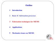
PME 4352 Homework 4 Due 11/25/11
PME 4352 Homework 4 Due 11/25/11
PME 4352 Homework 4 Due 11/25/11

You also want an ePaper? Increase the reach of your titles
YUMPU automatically turns print PDFs into web optimized ePapers that Google loves.
<strong>PME</strong> <strong>4352</strong> <strong>Homework</strong> 4 <strong>Due</strong> <strong>11</strong>/<strong>25</strong>/<strong>11</strong><br />
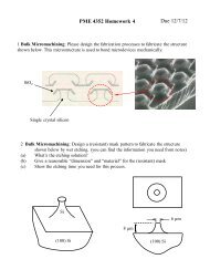
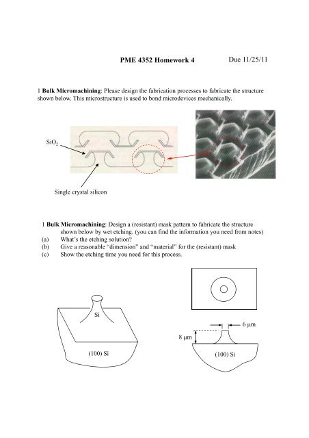
1 Bulk Micromachining: Please design the fabrication processes to fabricate the structure<br />
shown below. This microstructure is used to bond microdevices mechanically.<br />
SiO 2<br />
Single crystal silicon<br />
1 Bulk Micromachining: Design a (resistant) mask pattern to fabricate the structure<br />
shown below by wet etching. (you can find the information you need from notes)<br />
(a) What’s the etching solution?<br />
(b) Give a reasonable “dimension” and “material” for the (resistant) mask<br />
(c) Show the etching time you need for this process.<br />
Si<br />
6 m<br />
8 m<br />
(100) Si<br />
(100) Si
3. Draw the fabrication processes for the suspension shown below<br />
(100) substrate