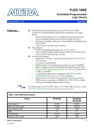
ALTERA CORPORATION (EPM1270GF256C5N) CPLD: MAX II Family
ALTERA CORPORATION (EPM1270GF256C5N) CPLD: MAX II Family
ALTERA CORPORATION (EPM1270GF256C5N) CPLD: MAX II Family

You also want an ePaper? Increase the reach of your titles
YUMPU automatically turns print PDFs into web optimized ePapers that Google loves.
Distributed by:<br />
www.Jameco.com ✦ 1-800-831-4242<br />
The content and copyrights of the attached<br />
material are the property of its owner.
Revision History<br />
Section I. <strong>MAX</strong> <strong>II</strong> Device<br />
<strong>Family</strong> Data Sheet<br />
This section provides designers with the data sheet specifications for<br />
<strong>MAX</strong> ® <strong>II</strong> devices. The chapters contain feature definitions of the internal<br />
architecture, Joint Test Action Group (JTAG) and in-system<br />
programmability (ISP) information, DC operating conditions, AC timing<br />
parameters, and ordering information for <strong>MAX</strong> <strong>II</strong> devices.<br />
This section includes the following chapters:<br />
■ Chapter 1. Introduction<br />
■ Chapter 2. <strong>MAX</strong> <strong>II</strong> Architecture<br />
■ Chapter 3. JTAG and In-System Programmability<br />
■ Chapter 4. Hot Socketing and Power-On Reset in <strong>MAX</strong> <strong>II</strong> Devices<br />
■ Chapter 5. DC and Switching Characteristics<br />
■ Chapter 6. Reference and Ordering Information<br />
Refer to each chapter for its own specific revision history. For information<br />
about when each chapter was updated, refer to the Chapter Revision<br />
Dates section, which appears in the complete handbook.<br />
Altera Corporation Section I–1
Revision History <strong>MAX</strong> <strong>II</strong> Device Handbook<br />
I–2 Altera Corporation
M<strong>II</strong>51001-1.7<br />
Introduction<br />
Features<br />
Chapter 1. Introduction<br />
The <strong>MAX</strong> ® <strong>II</strong> family of instant-on, non-volatile <strong>CPLD</strong>s is based on a<br />
0.18-µm, 6-layer-metal-flash process, with densities from 240 to 2,210<br />
logic elements (LEs) (128 to 2,210 equivalent macrocells) and non-volatile<br />
storage of 8 Kbits. <strong>MAX</strong> <strong>II</strong> devices offer high I/O counts, fast<br />
performance, and reliable fitting versus other <strong>CPLD</strong> architectures.<br />
Featuring MultiVolt core, a user flash memory (UFM) block, and<br />
enhanced in-system programmability (ISP), <strong>MAX</strong> <strong>II</strong> devices are designed<br />
to reduce cost and power while providing programmable solutions for<br />
applications such as bus bridging, I/O expansion, power-on reset (POR)<br />
and sequencing control, and device configuration control.<br />
The <strong>MAX</strong> <strong>II</strong> <strong>CPLD</strong> has the following features:<br />
■ Low-cost, low-power <strong>CPLD</strong><br />
■ Instant-on, non-volatile architecture<br />
■ Standby current as low as 29 µA<br />
■ Provides fast propagation delay and clock-to-output times<br />
■ Provides four global clocks with two clocks available per logic array<br />
block (LAB)<br />
■ UFM block up to 8 Kbits for non-volatile storage<br />
■ MultiVolt core enabling external supply voltages to the device of<br />
either 3.3 V/2.5 V or 1.8 V<br />
■ MultiVolt I/O interface supporting 3.3-V, 2.5-V, 1.8-V, and 1.5-V logic<br />
levels<br />
■ Bus-friendly architecture including programmable slew rate, drive<br />
strength, bus-hold, and programmable pull-up resistors<br />
■ Schmitt triggers enabling noise tolerant inputs (programmable per<br />
pin)<br />
■ Fully compliant with the Peripheral Component Interconnect Special<br />
Interest Group (PCI SIG) PCI Local Bus Specification, Revision 2.2 for<br />
3.3-V operation at 66 MHz<br />
■ Supports hot-socketing<br />
■ Built-in Joint Test Action Group (JTAG) boundary-scan test (BST)<br />
circuitry compliant with IEEE Std. 1149.1-1990<br />
■ ISP circuitry compliant with IEEE Std. 1532<br />
Altera Corporation 1–1<br />
December 2007
Features<br />
Table 1–1. <strong>MAX</strong> <strong>II</strong> <strong>Family</strong> Features<br />
Feature<br />
Table 1–1 shows the <strong>MAX</strong> <strong>II</strong> family features.<br />
EPM240<br />
EPM240G<br />
EPM570<br />
EPM570G<br />
EPM1270<br />
EPM1270G<br />
EPM2210<br />
EPM2210G<br />
EPM240Z EPM570Z<br />
LEs 240 570 1,270 2,210 240 570<br />
Typical Equivalent<br />
Macrocells<br />
192 440 980 1,700 192 440<br />
Equivalent Macrocell<br />
Range<br />
128 to 240 240 to 570 570 to 1,270 1,270 to 2,210 128 to 240 240 to 570<br />
UFM Size (bits) 8,192 8,192 8,192 8,192 8,192 8,192<br />
Maximum User I/O pins 80 160 212 272 80 160<br />
tPD1 (ns) (1) 4.7 5.4 6.2 7.0 7.5 9.0<br />
fCNT (MHz) (2) 304 304 304 304 152 152<br />
tSU (ns) 1.7 1.2 1.2 1.2 2.3 2.2<br />
tCO (ns) 4.3 4.5 4.6 4.6 6.5 6.7<br />
Notes to Table 1–1:<br />
(1) t PD1 represents a pin-to-pin delay for the worst case I/O placement with a full diagonal path across the device and<br />
combinational logic implemented in a single LUT and LAB that is adjacent to the output pin.<br />
(2) The maximum frequency is limited by the I/O standard on the clock input pin. The 16-bit counter critical delay<br />
will run faster than this number.<br />
f For more information about equivalent macrocells, refer to the <strong>MAX</strong> <strong>II</strong><br />
Logic Element to Macrocell Conversion Methodology white paper.<br />
<strong>MAX</strong> <strong>II</strong> and <strong>MAX</strong> <strong>II</strong>G devices are available in three speed grades: –3, –4,<br />
and –5, with –3 being the fastest. Similarly, <strong>MAX</strong> <strong>II</strong>Z devices are available<br />
in two speed grades: –6, –7, with –6 being faster. These speed grades<br />
represent the overall relative performance, not any specific timing<br />
parameter. For propagation delay timing numbers within each speed<br />
grade and density, refer to the DC and Switching Characteristics chapter in<br />
the <strong>MAX</strong> <strong>II</strong> Device Handbook.<br />
1–2 Core Version a.b.c variable Altera Corporation<br />
<strong>MAX</strong> <strong>II</strong> Device Handbook, Volume 1 December 2007
Table 1–2 shows <strong>MAX</strong> <strong>II</strong> device speed-grade offerings.<br />
Table 1–2. <strong>MAX</strong> <strong>II</strong> Speed Grades<br />
Device<br />
EPM240<br />
EPM240G<br />
EPM570<br />
EPM570G<br />
EPM1270<br />
EPM1270G<br />
EPM2210<br />
EPM2210G<br />
Speed Grade<br />
Introduction<br />
–3 –4 –5 –6 –7<br />
v v v — —<br />
v v v — —<br />
v v v — —<br />
v v v — —<br />
EPM240Z — — — v v<br />
EPM570Z — — — v v<br />
<strong>MAX</strong> <strong>II</strong> devices are available in space-saving FineLine BGA, Micro<br />
FineLine BGA, and thin quad flat pack (TQFP) packages (refer to<br />
Tables 1–3 and 1–4). <strong>MAX</strong> <strong>II</strong> devices support vertical migration within the<br />
same package (for example, you can migrate between the EPM570,<br />
EPM1270, and EPM2210 devices in the 256-pin FineLine BGA package).<br />
Vertical migration means that you can migrate to devices whose<br />
dedicated pins and JTAG pins are the same and power pins are subsets or<br />
supersets for a given package across device densities. The largest density<br />
in any package has the highest number of power pins; you must lay out<br />
for the largest planned density in a package to provide the necessary<br />
power pins for migration. For I/O pin migration across densities, cross<br />
reference the available I/O pins using the device pin-outs for all planned<br />
densities of a given package type to identify which I/O pins can be<br />
migrated. The Quartus ® <strong>II</strong> software can automatically cross-reference and<br />
place all pins for you when given a device migration list.<br />
Altera Corporation 1–3<br />
December 2007 <strong>MAX</strong> <strong>II</strong> Device Handbook, Volume 1
Features<br />
Table 1–3. <strong>MAX</strong> <strong>II</strong> Packages and User I/O Pins<br />
Device<br />
EPM240<br />
EPM240G<br />
EPM570<br />
EPM570G<br />
EPM1270<br />
EPM1270G<br />
EPM2210<br />
EPM2210G<br />
68-Pin<br />
Micro<br />
FineLine<br />
BGA (1)<br />
100-Pin<br />
Micro<br />
FineLine<br />
BGA (1)<br />
100-Pin<br />
FineLine<br />
BGA (1)<br />
100-Pin<br />
TQFP<br />
144-Pin<br />
TQFP<br />
144-Pin<br />
Micro<br />
FineLine<br />
BGA (1)<br />
256-Pin<br />
Micro<br />
FineLine<br />
BGA (1)<br />
256-Pin<br />
FineLine<br />
BGA<br />
324-Pin<br />
FineLine<br />
BGA<br />
— 80 80 80 — — — — —<br />
— 76 76 76 116 — 160 160 —<br />
— — — — 116 — 212 212 —<br />
— — — — — — — 204 272<br />
EPM240Z 54 80 — — — — — — —<br />
EPM570Z — 76 — — — 116 160 — —<br />
Note to Table 1–3:<br />
(1) Packages available in lead-free versions only.<br />
Table 1–4. <strong>MAX</strong> <strong>II</strong> TQFP, FineLine BGA, and Micro FineLine BGA Package Sizes<br />
Package<br />
68-Pin<br />
Micro<br />
FineLine<br />
BGA<br />
100-Pin<br />
Micro<br />
FineLine<br />
BGA<br />
100-Pin<br />
FineLine<br />
BGA<br />
100-Pin<br />
TQFP<br />
144-Pin<br />
TQFP<br />
144-Pin<br />
Micro<br />
FineLine<br />
BGA<br />
256-Pin<br />
Micro<br />
FineLine<br />
BGA<br />
256-Pin<br />
FineLine<br />
BGA<br />
324-Pin<br />
FineLine<br />
BGA<br />
Pitch (mm) 0.5 0.5 1 0.5 0.5 0.5 0.5 1 1<br />
Area (mm2) 25 36 121 256 484 49 121 289 361<br />
Length × width<br />
(mm × mm)<br />
5 × 5 6 × 6 11 × 11 16 × 16 22 × 22 7 × 7 11 × 11 17 × 17 19 × 19<br />
<strong>MAX</strong> <strong>II</strong> devices have an internal linear voltage regulator which supports<br />
external supply voltages of 3.3 V or 2.5 V, regulating the supply down to<br />
the internal operating voltage of 1.8 V. <strong>MAX</strong> <strong>II</strong>G and <strong>MAX</strong> <strong>II</strong>Z devices<br />
only accept 1.8 V as the external supply voltage. <strong>MAX</strong> <strong>II</strong>Z devices are<br />
pin-compatible with <strong>MAX</strong> <strong>II</strong>G devices in the 100-pin Micro FineLine BGA<br />
and 256-pin Micro FineLine BGA packages. Except for external supply<br />
1–4 Core Version a.b.c variable Altera Corporation<br />
<strong>MAX</strong> <strong>II</strong> Device Handbook, Volume 1 December 2007
Table 1–5. <strong>MAX</strong> <strong>II</strong> External Supply Voltages<br />
Referenced<br />
Documents<br />
Devices<br />
Introduction<br />
voltage requirements, <strong>MAX</strong> <strong>II</strong> and <strong>MAX</strong> <strong>II</strong> G devices have identical<br />
pin-outs and timing specifications. Table 1–5 shows the external supply<br />
voltages supported by the <strong>MAX</strong> <strong>II</strong> family.<br />
EPM240<br />
EPM570<br />
EPM1270<br />
EPM2210<br />
This chapter references the following documents:<br />
EPM240G<br />
EPM570G<br />
EPM1270G<br />
EPM2210G<br />
EPM240Z<br />
EPM570Z (1)<br />
MultiVolt core external supply voltage (VCCINT) (2) 3.3 V, 2.5 V 1.8 V<br />
MultiVolt I/O interface voltage levels (VCCIO) 1.5 V, 1.8 V, 2.5 V, 3.3 V 1.5 V, 1.8 V, 2.5 V, 3.3 V<br />
Notes to Table 1–5:<br />
(1) <strong>MAX</strong> <strong>II</strong>G and <strong>MAX</strong> <strong>II</strong>Z devices only accept 1.8 V on their VCCINT pins. The 1.8-V V CCINT external supply powers<br />
the device core directly.<br />
(2) <strong>MAX</strong> <strong>II</strong> devices operate internally at 1.8 V.<br />
■ DC and Switching Characteristics chapter in the <strong>MAX</strong> <strong>II</strong> Device<br />
Handbook<br />
■ <strong>MAX</strong> <strong>II</strong> Logic Element to Macrocell Conversion Methodology white paper<br />
Altera Corporation 1–5<br />
December 2007 <strong>MAX</strong> <strong>II</strong> Device Handbook, Volume 1
Document Revision History<br />
Document<br />
Revision History<br />
Table 1–6. Document Revision History<br />
Date and<br />
Document<br />
Version<br />
December 2007<br />
v1.7<br />
December 2006<br />
v1.6<br />
August 2006<br />
v1.5<br />
July 2006<br />
v1.4<br />
June 2005<br />
v1.3<br />
December 2004<br />
v1.2<br />
June 2004<br />
v1.1<br />
Table 1–6 shows the revision history for this chapter.<br />
● Updated Tables 1–1 through 1–5.<br />
● Added “Referenced Documents” section.<br />
Changes Made Summary of Changes<br />
Updated document with<br />
<strong>MAX</strong> <strong>II</strong>Z information.<br />
Added document revision history. —<br />
Minor update to features list. —<br />
Minor updates to tables. —<br />
Updated timing numbers in Table 1-1. —<br />
Updated timing numbers in Table 1-1. —<br />
Updated timing numbers in Table 1-1. —<br />
1–6 Core Version a.b.c variable Altera Corporation<br />
<strong>MAX</strong> <strong>II</strong> Device Handbook, Volume 1 December 2007
M<strong>II</strong>51002-2.1<br />
Introduction<br />
Functional<br />
Description<br />
Chapter 2. <strong>MAX</strong> <strong>II</strong><br />
Architecture<br />
This chapter describes the architecture of the <strong>MAX</strong> <strong>II</strong> device and contains<br />
the following sections:<br />
■ “Functional Description” on page 2–1<br />
■ “Logic Array Blocks” on page 2–5<br />
■ “Logic Elements” on page 2–8<br />
■ “MultiTrack Interconnect” on page 2–15<br />
■ “Global Signals” on page 2–20<br />
■ “User Flash Memory Block” on page 2–23<br />
■ “MultiVolt Core” on page 2–27<br />
■ “I/O Structure” on page 2–28<br />
<strong>MAX</strong> ® <strong>II</strong> devices contain a two-dimensional row- and column-based<br />
architecture to implement custom logic. Row and column interconnects<br />
provide signal interconnects between the logic array blocks (LABs).<br />
The logic array consists of LABs, with 10 logic elements (LEs) in each<br />
LAB. An LE is a small unit of logic providing efficient implementation of<br />
user logic functions. LABs are grouped into rows and columns across the<br />
device. The MultiTrack interconnect provides fast granular timing delays<br />
between LABs. The fast routing between LEs provides minimum timing<br />
delay for added levels of logic versus globally routed interconnect<br />
structures.<br />
The <strong>MAX</strong> <strong>II</strong> device I/O pins are fed by I/O elements (IOE) located at the<br />
ends of LAB rows and columns around the periphery of the device. Each<br />
IOE contains a bidirectional I/O buffer with several advanced features.<br />
I/O pins support Schmitt trigger inputs and various single-ended<br />
standards, such as 66-MHz, 32-bit PCI, and LVTTL.<br />
<strong>MAX</strong> <strong>II</strong> devices provide a global clock network. The global clock network<br />
consists of four global clock lines that drive throughout the entire device,<br />
providing clocks for all resources within the device. The global clock lines<br />
can also be used for control signals such as clear, preset, or output enable.<br />
Figure 2–1 shows a functional block diagram of the <strong>MAX</strong> <strong>II</strong> device.<br />
Altera Corporation Core Version a.b.c variable 2–1<br />
March 2008
Functional Description<br />
Figure 2–1. <strong>MAX</strong> <strong>II</strong> Device Block Diagram<br />
IOE<br />
IOE<br />
MultiTrack<br />
Interconnect<br />
IOE<br />
IOE<br />
IOE IOE<br />
Logic<br />
Element<br />
Logic<br />
Element<br />
Logic<br />
Element<br />
Logic<br />
Element<br />
MultiTrack<br />
Interconnect<br />
IOE IOE<br />
Logic<br />
Element<br />
Logic<br />
Element<br />
Logic<br />
Element<br />
Logic<br />
Element<br />
IOE IOE<br />
Logic<br />
Element<br />
Logic<br />
Element<br />
Logic<br />
Element<br />
Logic<br />
Element<br />
Logic Array<br />
BLock (LAB)<br />
Each <strong>MAX</strong> <strong>II</strong> device contains a flash memory block within its floorplan.<br />
On the EPM240 device, this block is located on the left side of the device.<br />
On the EPM570, EPM1270, and EPM2210 devices, the flash memory block<br />
is located on the bottom-left area of the device. The majority of this flash<br />
memory storage is partitioned as the dedicated configuration flash<br />
memory (CFM) block. The CFM block provides the non-volatile storage<br />
for all of the SRAM configuration information. The CFM automatically<br />
downloads and configures the logic and I/O at power-up, providing<br />
instant-on operation.<br />
f For more information about configuration upon power-up, refer to the<br />
Hot Socketing and Power-On Reset in <strong>MAX</strong> <strong>II</strong> Devices chapter in the <strong>MAX</strong> <strong>II</strong><br />
Device Handbook.<br />
A portion of the flash memory within the <strong>MAX</strong> <strong>II</strong> device is partitioned<br />
into a small block for user data. This user flash memory (UFM) block<br />
provides 8,192 bits of general-purpose user storage. The UFM provides<br />
programmable port connections to the logic array for reading and<br />
writing. There are three LAB rows adjacent to this block, with column<br />
numbers varying by device.<br />
2–2Core Version a.b.c variable Altera Corporation<br />
<strong>MAX</strong> <strong>II</strong> Device Handbook, Volume 1 March 2008
Table 2–1. <strong>MAX</strong> <strong>II</strong> Device Resources<br />
Devices UFM Blocks LAB Columns<br />
<strong>MAX</strong> <strong>II</strong> Architecture<br />
Table 2–1 shows the number of LAB rows and columns in each device, as<br />
well as the number of LAB rows and columns adjacent to the flash<br />
memory area in the EPM570, EPM1270, and EPM2210 devices. The long<br />
LAB rows are full LAB rows that extend from one side of row I/O blocks<br />
to the other. The short LAB rows are adjacent to the UFM block; their<br />
length is shown as width in LAB columns.<br />
Long LAB Rows<br />
LAB Rows<br />
Short LAB Rows<br />
(Width) (1)<br />
Total LABs<br />
EPM240 1 6 4 — 24<br />
EPM570 1 12 4 3 (3) 57<br />
EPM1270 1 16 7 3 (5) 127<br />
EPM2210 1 20 10 3 (7) 221<br />
Note to Table 2–1:<br />
(1) The width is the number of LAB columns in length.<br />
Altera Corporation 2–3<br />
March 2008 <strong>MAX</strong> <strong>II</strong> Device Handbook, Volume 1
Functional Description<br />
Figure 2–2. <strong>MAX</strong> <strong>II</strong> Device Floorplan Note (1)<br />
I/O Blocks<br />
I/O Blocks<br />
Logic Array<br />
Blocks<br />
2 GCLK<br />
Inputs<br />
I/O Blocks<br />
Figure 2–2 shows a floorplan of a <strong>MAX</strong> <strong>II</strong> device.<br />
UFM Block<br />
CFM Block<br />
Logic Array<br />
Blocks<br />
2 GCLK<br />
Inputs<br />
Note to Figure 2–2:<br />
(1) The device shown is an EPM570 device. EPM1270 and EPM2210 devices have a similar floorplan with more LABs.<br />
For EPM240 devices, the CFM and UFM blocks are located on the left side of the device.<br />
2–4Core Version a.b.c variable Altera Corporation<br />
<strong>MAX</strong> <strong>II</strong> Device Handbook, Volume 1 March 2008
Logic Array<br />
Blocks<br />
Figure 2–3. <strong>MAX</strong> <strong>II</strong> LAB Structure<br />
Fast I/O connection<br />
to IOE (1)<br />
DirectLink<br />
interconnect from<br />
adjacent LAB<br />
or IOE<br />
DirectLink<br />
interconnect to<br />
adjacent LAB<br />
or IOE<br />
Note to Figure 2–3:<br />
(1) Only from LABs adjacent to IOEs.<br />
<strong>MAX</strong> <strong>II</strong> Architecture<br />
Each LAB consists of 10 LEs, LE carry chains, LAB control signals, a local<br />
interconnect, a look-up table (LUT) chain, and register chain connection<br />
lines. There are 26 possible unique inputs into an LAB, with an additional<br />
10 local feedback input lines fed by LE outputs in the same LAB. The local<br />
interconnect transfers signals between LEs in the same LAB. LUT chain<br />
connections transfer the output of one LE’s LUT to the adjacent LE for fast<br />
sequential LUT connections within the same LAB. Register chain<br />
connections transfer the output of one LE’s register to the adjacent LE’s<br />
register within an LAB. The Quartus ® <strong>II</strong> software places associated logic<br />
within an LAB or adjacent LABs, allowing the use of local, LUT chain,<br />
and register chain connections for performance and area efficiency.<br />
Figure 2–3 shows the <strong>MAX</strong> <strong>II</strong> LAB.<br />
Logic Element<br />
LE0<br />
LE1<br />
LE2<br />
LE3<br />
LE4<br />
LE5<br />
LE6<br />
LE7<br />
LE8<br />
LE9<br />
LAB<br />
Local Interconnect<br />
Row Interconnect<br />
Column Interconnect<br />
Fast I/O connection<br />
to IOE (1)<br />
DirectLink<br />
interconnect from<br />
adjacent LAB<br />
or IOE<br />
DirectLink<br />
interconnect to<br />
adjacent LAB<br />
or IOE<br />
Altera Corporation 2–5<br />
March 2008 <strong>MAX</strong> <strong>II</strong> Device Handbook, Volume 1
Logic Array Blocks<br />
Figure 2–4. DirectLink Connection<br />
DirectLink interconnect from<br />
left LAB or IOE output<br />
DirectLink<br />
interconnect<br />
to left<br />
LAB Interconnects<br />
The LAB local interconnect can drive LEs within the same LAB. The LAB<br />
local interconnect is driven by column and row interconnects and LE<br />
outputs within the same LAB. Neighboring LABs, from the left and right,<br />
can also drive an LAB’s local interconnect through the DirectLink<br />
connection. The DirectLink connection feature minimizes the use of row<br />
and column interconnects, providing higher performance and flexibility.<br />
Each LE can drive 30 other LEs through fast local and DirectLink<br />
interconnects. Figure 2–4 shows the DirectLink connection.<br />
Local<br />
Interconnect<br />
Logic Element<br />
LAB Control Signals<br />
Each LAB contains dedicated logic for driving control signals to its LEs.<br />
The control signals include two clocks, two clock enables, two<br />
asynchronous clears, a synchronous clear, an asynchronous preset/load,<br />
a synchronous load, and add/subtract control signals, providing a<br />
maximum of 10 control signals at a time. Although synchronous load and<br />
clear signals are generally used when implementing counters, they can<br />
also be used with other functions.<br />
2–6Core Version a.b.c variable Altera Corporation<br />
<strong>MAX</strong> <strong>II</strong> Device Handbook, Volume 1 March 2008<br />
LE0<br />
LE1<br />
LE2<br />
LE3<br />
LE4<br />
LE5<br />
LE6<br />
LE7<br />
LE8<br />
LE9<br />
LAB<br />
DirectLink interconnect from<br />
right LAB or IOE output<br />
DirectLink<br />
interconnect<br />
to right
Figure 2–5. LAB-Wide Control Signals<br />
Dedicated<br />
LAB Column<br />
Clocks<br />
Local<br />
Interconnect<br />
Local<br />
Interconnect<br />
Local<br />
Interconnect<br />
Local<br />
Interconnect<br />
Local<br />
Interconnect<br />
Local<br />
Interconnect<br />
4<br />
<strong>MAX</strong> <strong>II</strong> Architecture<br />
Each LAB can use two clocks and two clock enable signals. Each LAB’s<br />
clock and clock enable signals are linked. For example, any LE in a<br />
particular LAB using the labclk1 signal also uses labclkena1. If the<br />
LAB uses both the rising and falling edges of a clock, it also uses both<br />
LAB-wide clock signals. Deasserting the clock enable signal turns off the<br />
LAB-wide clock.<br />
Each LAB can use two asynchronous clear signals and an asynchronous<br />
load /preset signal. By default, the Quartus <strong>II</strong> software uses a NOT gate<br />
push-back technique to achieve preset. If you disable the NOT gate<br />
push-back option or assign a given register to power-up high using the<br />
Quartus <strong>II</strong> software, the preset is then achieved using the asynchronous<br />
load signal with asynchronous load data input tied high.<br />
With the LAB-wide addnsub control signal, a single LE can implement a<br />
one-bit adder and subtractor. This saves LE resources and improves<br />
performance for logic functions such as correlators and signed<br />
multipliers that alternate between addition and subtraction depending<br />
on data.<br />
The LAB column clocks [3..0], driven by the global clock network, and<br />
LAB local interconnect generate the LAB-wide control signals. The<br />
MultiTrack interconnect structure drives the LAB local interconnect for<br />
non-global control signal generation. The MultiTrack interconnect’s<br />
inherent low skew allows clock and control signal distribution in addition<br />
to data. Figure 2–5 shows the LAB control signal generation circuit.<br />
labclk1<br />
labclkena1<br />
labclk2<br />
labclkena2<br />
asyncload<br />
or labpre<br />
syncload<br />
Altera Corporation 2–7<br />
March 2008 <strong>MAX</strong> <strong>II</strong> Device Handbook, Volume 1<br />
labclr1<br />
labclr2<br />
synclr<br />
addnsub
Logic Elements<br />
Logic Elements The smallest unit of logic in the <strong>MAX</strong> <strong>II</strong> architecture, the LE, is compact<br />
and provides advanced features with efficient logic utilization. Each LE<br />
contains a four-input LUT, which is a function generator that can<br />
implement any function of four variables. In addition, each LE contains a<br />
programmable register and carry chain with carry-select capability. A<br />
single LE also supports dynamic single-bit addition or subtraction mode<br />
selectable by an LAB-wide control signal. Each LE drives all types of<br />
interconnects: local, row, column, LUT chain, register chain, and<br />
DirectLink interconnects. See Figure 2–6.<br />
Figure 2–6. <strong>MAX</strong> <strong>II</strong> LE<br />
addnsub<br />
data1<br />
data2<br />
data3<br />
data4<br />
labclr1<br />
labclr2<br />
labpre/aload<br />
Chip-Wide<br />
Reset (DEV_CLRn)<br />
labclk1<br />
labclk2<br />
labclkena1<br />
labclkena2<br />
LAB Carry-In<br />
Carry-In1<br />
Carry-In0<br />
Asynchronous<br />
Clear/Preset/<br />
Load Logic<br />
Clock and<br />
Clock Enable<br />
Select<br />
Look-Up<br />
Table<br />
(LUT)<br />
Carry<br />
Chain<br />
Register chain<br />
routing from<br />
previous LE<br />
LAB-wide<br />
Synchronous<br />
Load<br />
LAB-wide<br />
Synchronous<br />
Clear<br />
Carry-Out0<br />
Carry-Out1<br />
Synchronous<br />
Load and<br />
Clear Logic<br />
LAB Carry-Out<br />
Register Bypass<br />
Packed<br />
Register Select<br />
PRN/ALD<br />
D Q<br />
Programmable<br />
Register<br />
Row, column,<br />
and DirectLink<br />
routing<br />
Row, column,<br />
and DirectLink<br />
routing<br />
Each LE’s programmable register can be configured for D, T, JK, or SR<br />
operation. Each register has data, true asynchronous load data, clock,<br />
clock enable, clear, and asynchronous load/preset inputs. Global signals,<br />
general-purpose I/O pins, or any LE can drive the register’s clock and<br />
clear control signals. Either general-purpose I/O pins or LEs can drive the<br />
clock enable, preset, asynchronous load, and asynchronous data. The<br />
2–8Core Version a.b.c variable Altera Corporation<br />
<strong>MAX</strong> <strong>II</strong> Device Handbook, Volume 1 March 2008<br />
ADATA<br />
ENA<br />
CLRN<br />
Register<br />
Feedback<br />
LUT chain<br />
routing to next LE<br />
Local routing<br />
Register chain<br />
output
<strong>MAX</strong> <strong>II</strong> Architecture<br />
asynchronous load data input comes from the data3 input of the LE. For<br />
combinational functions, the LUT output bypasses the register and drives<br />
directly to the LE outputs.<br />
Each LE has three outputs that drive the local, row, and column routing<br />
resources. The LUT or register output can drive these three outputs<br />
independently. Two LE outputs drive column or row and DirectLink<br />
routing connections and one drives local interconnect resources. This<br />
allows the LUT to drive one output while the register drives another<br />
output. This register packing feature improves device utilization because<br />
the device can use the register and the LUT for unrelated functions.<br />
Another special packing mode allows the register output to feed back into<br />
the LUT of the same LE so that the register is packed with its own fan-out<br />
LUT. This provides another mechanism for improved fitting. The LE can<br />
also drive out registered and unregistered versions of the LUT output.<br />
LUT Chain and Register Chain<br />
In addition to the three general routing outputs, the LEs within an LAB<br />
have LUT chain and register chain outputs. LUT chain connections allow<br />
LUTs within the same LAB to cascade together for wide input functions.<br />
Register chain outputs allow registers within the same LAB to cascade<br />
together. The register chain output allows an LAB to use LUTs for a single<br />
combinational function and the registers to be used for an unrelated shift<br />
register implementation. These resources speed up connections between<br />
LABs while saving local interconnect resources. Refer to “MultiTrack<br />
Interconnect” on page 2–15 for more information about LUT chain and<br />
register chain connections.<br />
addnsub Signal<br />
The LE’s dynamic adder/subtractor feature saves logic resources by<br />
using one set of LEs to implement both an adder and a subtractor. This<br />
feature is controlled by the LAB-wide control signal addnsub. The<br />
addnsub signal sets the LAB to perform either A + B or A – B. The LUT<br />
computes addition; subtraction is computed by adding the two’s<br />
complement of the intended subtractor. The LAB-wide signal converts to<br />
two’s complement by inverting the B bits within the LAB and setting<br />
carry-in to 1, which adds one to the least significant bit (LSB). The LSB of<br />
an adder/subtractor must be placed in the first LE of the LAB, where the<br />
LAB-wide addnsub signal automatically sets the carry-in to 1. The<br />
Quartus <strong>II</strong> Compiler automatically places and uses the adder/subtractor<br />
feature when using adder/subtractor parameterized functions.<br />
Altera Corporation 2–9<br />
March 2008 <strong>MAX</strong> <strong>II</strong> Device Handbook, Volume 1
Logic Elements<br />
LE Operating Modes<br />
The <strong>MAX</strong> <strong>II</strong> LE can operate in one of the following modes:<br />
■ “Normal Mode”<br />
■ “Dynamic Arithmetic Mode”<br />
Each mode uses LE resources differently. In each mode, eight available<br />
inputs to the LE, the four data inputs from the LAB local interconnect,<br />
carry-in0 and carry-in1 from the previous LE, the LAB carry-in<br />
from the previous carry-chain LAB, and the register chain connection are<br />
directed to different destinations to implement the desired logic function.<br />
LAB-wide signals provide clock, asynchronous clear, asynchronous<br />
preset/load, synchronous clear, synchronous load, and clock enable<br />
control for the register. These LAB-wide signals are available in all LE<br />
modes. The addnsub control signal is allowed in arithmetic mode.<br />
The Quartus <strong>II</strong> software, in conjunction with parameterized functions<br />
such as library of parameterized modules (LPM) functions, automatically<br />
chooses the appropriate mode for common functions such as counters,<br />
adders, subtractors, and arithmetic functions.<br />
Normal Mode<br />
The normal mode is suitable for general logic applications and<br />
combinational functions. In normal mode, four data inputs from the LAB<br />
local interconnect are inputs to a four-input LUT (see Figure 2–7). The<br />
Quartus <strong>II</strong> Compiler automatically selects the carry-in or the data3<br />
signal as one of the inputs to the LUT. Each LE can use LUT chain<br />
connections to drive its combinational output directly to the next LE in<br />
the LAB. Asynchronous load data for the register comes from the data3<br />
input of the LE. LEs in normal mode support packed registers.<br />
2–10Core Version a.b.c variable Altera Corporation<br />
<strong>MAX</strong> <strong>II</strong> Device Handbook, Volume 1 March 2008
Figure 2–7. LE in Normal Mode<br />
addnsub (LAB Wide)<br />
(1)<br />
data1<br />
data2<br />
data3<br />
cin (from cout<br />
of previous LE)<br />
data4<br />
Note to Figure 2–7:<br />
(1) This signal is only allowed in normal mode if the LE is at the end of an adder/subtractor chain.<br />
Dynamic Arithmetic Mode<br />
<strong>MAX</strong> <strong>II</strong> Architecture<br />
The dynamic arithmetic mode is ideal for implementing adders, counters,<br />
accumulators, wide parity functions, and comparators. An LE in dynamic<br />
arithmetic mode uses four 2-input LUTs configurable as a dynamic<br />
adder/subtractor. The first two 2-input LUTs compute two summations<br />
based on a possible carry-in of 1 or 0; the other two LUTs generate carry<br />
outputs for the two chains of the carry-select circuitry. As shown in<br />
Figure 2–8, the LAB carry-in signal selects either the carry-in0 or<br />
carry-in1 chain. The selected chain’s logic level in turn determines<br />
which parallel sum is generated as a combinational or registered output.<br />
For example, when implementing an adder, the sum output is the<br />
selection of two possible calculated sums:<br />
data1 + data2 + carry in0<br />
or<br />
4-Input<br />
LUT<br />
Register Feedback<br />
Register chain<br />
connection<br />
sload<br />
(LAB Wide)<br />
clock (LAB Wide)<br />
ena (LAB Wide)<br />
aclr (LAB Wide)<br />
sclear<br />
(LAB Wide)<br />
data1 + data2 + carry-in1<br />
aload<br />
(LAB Wide)<br />
ALD/PRE<br />
ADATA Q<br />
D<br />
ENA<br />
CLRN<br />
Row, column, and<br />
DirectLink routing<br />
Row, column, and<br />
DirectLink routing<br />
Local routing<br />
LUT chain<br />
connection<br />
Register<br />
chain output<br />
Altera Corporation 2–11<br />
March 2008 <strong>MAX</strong> <strong>II</strong> Device Handbook, Volume 1
Logic Elements<br />
Figure 2–8. LE in Dynamic Arithmetic Mode<br />
LAB Carry-In<br />
Carry-In0<br />
Carry-In1<br />
addnsub<br />
(LAB Wide)<br />
(1)<br />
data1 LUT<br />
data2<br />
data3<br />
The other two LUTs use the data1 and data2 signals to generate two<br />
possible carry-out signals: one for a carry of 1 and the other for a carry of<br />
0. The carry-in0 signal acts as the carry-select for the carry-out0<br />
output and carry-in1 acts as the carry-select for the carry-out1<br />
output. LEs in arithmetic mode can drive out registered and unregistered<br />
versions of the LUT output.<br />
The dynamic arithmetic mode also offers clock enable, counter enable,<br />
synchronous up/down control, synchronous clear, synchronous load,<br />
and dynamic adder/subtractor options. The LAB local interconnect data<br />
inputs generate the counter enable and synchronous up/down control<br />
signals. The synchronous clear and synchronous load options are<br />
LAB-wide signals that affect all registers in the LAB. The Quartus <strong>II</strong><br />
software automatically places any registers that are not used by the<br />
counter into other LABs. The addnsub LAB-wide signal controls<br />
whether the LE acts as an adder or subtractor.<br />
LUT<br />
LUT<br />
LUT<br />
Carry-Out0<br />
Register chain<br />
connection<br />
Carry-Out1<br />
sload<br />
(LAB Wide)<br />
clock (LAB Wide)<br />
ena (LAB Wide)<br />
aclr (LAB Wide)<br />
sclear<br />
(LAB Wide)<br />
Register Feedback<br />
aload<br />
(LAB Wide)<br />
ALD/PRE<br />
ADATA Q<br />
D<br />
ENA<br />
CLRN<br />
Note to Figure 2–8:<br />
(1) The addnsub signal is tied to the carry input for the first LE of a carry chain only.<br />
Row, column, and<br />
direct link routing<br />
Row, column, and<br />
direct link routing<br />
Local routing<br />
LUT chain<br />
connection<br />
Register<br />
chain output<br />
2–12Core Version a.b.c variable Altera Corporation<br />
<strong>MAX</strong> <strong>II</strong> Device Handbook, Volume 1 March 2008
Carry-Select Chain<br />
<strong>MAX</strong> <strong>II</strong> Architecture<br />
The carry-select chain provides a very fast carry-select function between<br />
LEs in dynamic arithmetic mode. The carry-select chain uses the<br />
redundant carry calculation to increase the speed of carry functions. The<br />
LE is configured to calculate outputs for a possible carry-in of 0 and<br />
carry-in of 1 in parallel. The carry-in0 and carry-in1 signals from a<br />
lower-order bit feed forward into the higher-order bit via the parallel<br />
carry chain and feed into both the LUT and the next portion of the carry<br />
chain. Carry-select chains can begin in any LE within an LAB.<br />
The speed advantage of the carry-select chain is in the parallel<br />
precomputation of carry chains. Since the LAB carry-in selects the<br />
precomputed carry chain, not every LE is in the critical path. Only the<br />
propagation delays between LAB carry-in generation (LE 5 and LE 10) are<br />
now part of the critical path. This feature allows the <strong>MAX</strong> <strong>II</strong> architecture<br />
to implement high-speed counters, adders, multipliers, parity functions,<br />
and comparators of arbitrary width.<br />
Figure 2–9 shows the carry-select circuitry in an LAB for a 10-bit full<br />
adder. One portion of the LUT generates the sum of two bits using the<br />
input signals and the appropriate carry-in bit; the sum is routed to the<br />
output of the LE. The register can be bypassed for simple adders or used<br />
for accumulator functions. Another portion of the LUT generates<br />
carry-out bits. An LAB-wide carry-in bit selects which chain is used for<br />
the addition of given inputs. The carry-in signal for each chain,<br />
carry-in0 or carry-in1, selects the carry-out to carry forward to the<br />
carry-in signal of the next-higher-order bit. The final carry-out signal is<br />
routed to an LE, where it is fed to local, row, or column interconnects.<br />
Altera Corporation 2–13<br />
March 2008 <strong>MAX</strong> <strong>II</strong> Device Handbook, Volume 1
Logic Elements<br />
Figure 2–9. Carry-Select Chain<br />
LAB Carry-In<br />
A1<br />
B1<br />
A2<br />
B2<br />
A3<br />
B3<br />
A4<br />
B4<br />
A5<br />
B5<br />
A6<br />
B6<br />
A7<br />
B7<br />
A8<br />
B8<br />
A9<br />
B9<br />
A10<br />
B10<br />
0 1<br />
LE0<br />
LE1<br />
LE2<br />
LE3<br />
LE4<br />
0 1<br />
LE5<br />
LE6<br />
LE7<br />
LE8<br />
LE9<br />
LAB Carry-Out<br />
Sum1<br />
Sum2<br />
Sum3<br />
Sum4<br />
Sum5<br />
Sum6<br />
Sum7<br />
Sum8<br />
Sum9<br />
Sum10<br />
To top of adjacent LAB<br />
LAB Carry-In<br />
Carry-In0<br />
Carry-In1<br />
data1<br />
data2<br />
The Quartus <strong>II</strong> software automatically creates carry chain logic during<br />
design processing, or you can create it manually during design entry.<br />
Parameterized functions such as LPM functions automatically take<br />
advantage of carry chains for the appropriate functions. The Quartus <strong>II</strong><br />
software creates carry chains longer than 10 LEs by linking adjacent LABs<br />
within the same row together automatically. A carry chain can extend<br />
horizontally up to one full LAB row, but does not extend between LAB<br />
rows.<br />
2–14Core Version a.b.c variable Altera Corporation<br />
<strong>MAX</strong> <strong>II</strong> Device Handbook, Volume 1 March 2008<br />
LUT<br />
LUT<br />
LUT<br />
LUT<br />
Carry-Out0 Carry-Out1<br />
Sum
MultiTrack<br />
Interconnect<br />
Clear and Preset Logic Control<br />
<strong>MAX</strong> <strong>II</strong> Architecture<br />
LAB-wide signals control the logic for the register’s clear and preset<br />
signals. The LE directly supports an asynchronous clear and preset<br />
function. The register preset is achieved through the asynchronous load<br />
of a logic high. <strong>MAX</strong> <strong>II</strong> devices support simultaneous<br />
preset/asynchronous load and clear signals. An asynchronous clear<br />
signal takes precedence if both signals are asserted simultaneously. Each<br />
LAB supports up to two clears and one preset signal.<br />
In addition to the clear and preset ports, <strong>MAX</strong> <strong>II</strong> devices provide a<br />
chip-wide reset pin (DEV_CLRn) that resets all registers in the device. An<br />
option set before compilation in the Quartus <strong>II</strong> software controls this pin.<br />
This chip-wide reset overrides all other control signals and uses its own<br />
dedicated routing resources (that is, it does not use any of the four global<br />
resources). Driving this signal low before or during power-up prevents<br />
user mode from releasing clears within the design. This allows you to<br />
control when clear is released on a device that has just been powered-up.<br />
If not set for its chip-wide reset function, the DEV_CLRn pin is a regular<br />
I/O pin.<br />
By default, all registers in <strong>MAX</strong> <strong>II</strong> devices are set to power-up low.<br />
However, this power-up state can be set to high on individual registers<br />
during design entry using the Quartus <strong>II</strong> software.<br />
In the <strong>MAX</strong> <strong>II</strong> architecture, connections between LEs, the UFM, and<br />
device I/O pins are provided by the MultiTrack interconnect structure.<br />
The MultiTrack interconnect consists of continuous,<br />
performance-optimized routing lines used for inter- and intra-design<br />
block connectivity. The Quartus <strong>II</strong> Compiler automatically places critical<br />
design paths on faster interconnects to improve design performance.<br />
The MultiTrack interconnect consists of row and column interconnects<br />
that span fixed distances. A routing structure with fixed length resources<br />
for all devices allows predictable and short delays between logic levels<br />
instead of large delays associated with global or long routing lines.<br />
Dedicated row interconnects route signals to and from LABs within the<br />
same row. These row resources include:<br />
■ DirectLink interconnects between LABs<br />
■ R4 interconnects traversing four LABs to the right or left<br />
The DirectLink interconnect allows an LAB to drive into the local<br />
interconnect of its left and right neighbors. The DirectLink interconnect<br />
provides fast communication between adjacent LABs and/or blocks<br />
without using row interconnect resources.<br />
Altera Corporation 2–15<br />
March 2008 <strong>MAX</strong> <strong>II</strong> Device Handbook, Volume 1
MultiTrack Interconnect<br />
Figure 2–10. R4 Interconnect Connections<br />
Notes to Figure 2–10:<br />
(1) C4 interconnects can drive R4 interconnects.<br />
(2) This pattern is repeated for every LAB in the LAB row.<br />
The R4 interconnects span four LABs and are used for fast row<br />
connections in a four-LAB region. Every LAB has its own set of R4<br />
interconnects to drive either left or right. Figure 2–10 shows R4<br />
interconnect connections from an LAB. R4 interconnects can drive and be<br />
driven by row IOEs. For LAB interfacing, a primary LAB or horizontal<br />
LAB neighbor can drive a given R4 interconnect. For R4 interconnects that<br />
drive to the right, the primary LAB and right neighbor can drive on to the<br />
interconnect. For R4 interconnects that drive to the left, the primary LAB<br />
and its left neighbor can drive on to the interconnect. R4 interconnects can<br />
drive other R4 interconnects to extend the range of LABs they can drive.<br />
R4 interconnects can also drive C4 interconnects for connections from one<br />
row to another.<br />
Adjacent LAB can<br />
drive onto another<br />
LAB’s R4 Interconnect<br />
R4 Interconnect<br />
Driving Left<br />
LAB<br />
Neighbor<br />
Primary<br />
LAB (2)<br />
C4 Column Interconnects (1)<br />
LAB<br />
Neighbor<br />
R4 Interconnect<br />
Driving Right<br />
2–16Core Version a.b.c variable Altera Corporation<br />
<strong>MAX</strong> <strong>II</strong> Device Handbook, Volume 1 March 2008
<strong>MAX</strong> <strong>II</strong> Architecture<br />
The column interconnect operates similarly to the row interconnect. Each<br />
column of LABs is served by a dedicated column interconnect, which<br />
vertically routes signals to and from LABs and row and column IOEs.<br />
These column resources include:<br />
■ LUT chain interconnects within an LAB<br />
■ Register chain interconnects within an LAB<br />
■ C4 interconnects traversing a distance of four LABs in an up and<br />
down direction<br />
<strong>MAX</strong> <strong>II</strong> devices include an enhanced interconnect structure within LABs<br />
for routing LE output to LE input connections faster using LUT chain<br />
connections and register chain connections. The LUT chain connection<br />
allows the combinational output of an LE to directly drive the fast input<br />
of the LE right below it, bypassing the local interconnect. These resources<br />
can be used as a high-speed connection for wide fan-in functions from<br />
LE 1 to LE 10 in the same LAB. The register chain connection allows the<br />
register output of one LE to connect directly to the register input of the<br />
next LE in the LAB for fast shift registers. The Quartus <strong>II</strong> Compiler<br />
automatically takes advantage of these resources to improve utilization<br />
and performance. Figure 2–11 shows the LUT chain and register chain<br />
interconnects.<br />
Altera Corporation 2–17<br />
March 2008 <strong>MAX</strong> <strong>II</strong> Device Handbook, Volume 1
MultiTrack Interconnect<br />
Figure 2–11. LUT Chain and Register Chain Interconnects<br />
LUT Chain<br />
Routing to<br />
Adjacent LE<br />
Local<br />
Interconnect<br />
Local Interconnect<br />
Routing Among LEs<br />
in the LAB<br />
The C4 interconnects span four LABs up or down from a source LAB.<br />
Every LAB has its own set of C4 interconnects to drive either up or down.<br />
Figure 2–12 shows the C4 interconnect connections from an LAB in a<br />
column. The C4 interconnects can drive and be driven by column and row<br />
IOEs. For LAB interconnection, a primary LAB or its vertical LAB<br />
neighbor can drive a given C4 interconnect. C4 interconnects can drive<br />
each other to extend their range as well as drive row interconnects for<br />
column-to-column connections.<br />
2–18Core Version a.b.c variable Altera Corporation<br />
<strong>MAX</strong> <strong>II</strong> Device Handbook, Volume 1 March 2008<br />
LE0<br />
LE1<br />
LE2<br />
LE3<br />
LE4<br />
LE5<br />
LE6<br />
LE7<br />
LE8<br />
LE9<br />
Register Chain<br />
Routing to Adjacent<br />
LE's Register Input
Figure 2–12. C4 Interconnect Connections Note (1)<br />
Row<br />
Interconnect<br />
Adjacent LAB can<br />
drive onto neighboring<br />
LAB's C4 interconnect<br />
Local<br />
Interconnect<br />
Note to Figure 2–12:<br />
(1) Each C4 interconnect can drive either up or down four rows.<br />
C4 Interconnect<br />
Driving Down<br />
<strong>MAX</strong> <strong>II</strong> Architecture<br />
C4 Interconnect<br />
Drives Local and R4<br />
Interconnects<br />
Up to Four Rows<br />
C4 Interconnect<br />
Driving Up<br />
Altera Corporation 2–19<br />
March 2008 <strong>MAX</strong> <strong>II</strong> Device Handbook, Volume 1<br />
LAB
Global Signals<br />
Table 2–2. <strong>MAX</strong> <strong>II</strong> Device Routing Scheme<br />
Source<br />
LUT<br />
Chain<br />
Global Signals<br />
Register<br />
Chain<br />
The UFM block communicates with the logic array similar to LAB-to-LAB<br />
interfaces. The UFM block connects to row and column interconnects and<br />
has local interconnect regions driven by row and column interconnects.<br />
This block also has DirectLink interconnects for fast connections to and<br />
from a neighboring LAB. For more information about the UFM interface<br />
to the logic array, see “User Flash Memory Block” on page 2–23.<br />
Table 2–2 shows the <strong>MAX</strong> <strong>II</strong> device routing scheme.<br />
Local<br />
(1)<br />
DirectLink<br />
(1)<br />
Destination<br />
R4 (1) C4 (1) LE UFM<br />
Block<br />
Column<br />
IOE<br />
Each <strong>MAX</strong> <strong>II</strong> device has four dual-purpose dedicated clock pins<br />
(GCLK[3..0], two pins on the left side and two pins on the right side)<br />
that drive the global clock network for clocking, as shown in Figure 2–13.<br />
These four pins can also be used as general-purpose I/O if they are not<br />
used to drive the global clock network.<br />
The four global clock lines in the global clock network drive throughout<br />
the entire device. The global clock network can provide clocks for all<br />
resources within the device including LEs, LAB local interconnect, IOEs,<br />
and the UFM block. The global clock lines can also be used for global<br />
2–20Core Version a.b.c variable Altera Corporation<br />
<strong>MAX</strong> <strong>II</strong> Device Handbook, Volume 1 March 2008<br />
Row<br />
IOE<br />
Fast I/O<br />
(1)<br />
LUT Chain — — — — — — v — — — —<br />
Register<br />
Chain<br />
— — — — — — v — — — —<br />
Local<br />
Interconnect<br />
DirectLink<br />
Interconnect<br />
R4<br />
Interconnect<br />
C4<br />
Interconnect<br />
— — — — — — v v v v —<br />
— — v — — — — — — — —<br />
— — v — v v — — — — —<br />
— — v — v v — — — — —<br />
LE v v v v v v — — v v v<br />
UFM Block — — v v v v — — — — —<br />
Column IOE — — — — — v — — — — —<br />
Row IOE — — — v v v — — — — —<br />
Note to Table 2–2:<br />
(1) These categories are interconnects.
<strong>MAX</strong> <strong>II</strong> Architecture<br />
control signals, such as clock enables, synchronous or asynchronous<br />
clears, presets, output enables, or protocol control signals such as TRDY<br />
and IRDY for PCI. Internal logic can drive the global clock network for<br />
internally-generated global clocks and control signals. Figure 2–13 shows<br />
the various sources that drive the global clock network.<br />
Figure 2–13. Global Clock Generation<br />
GCLK0<br />
GCLK1<br />
GCLK2<br />
GCLK3<br />
Logic Array(1)<br />
Note to Figure 2–13:<br />
(1) Any I/O pin can use a MultiTrack interconnect to route as a logic array-generated<br />
global clock signal.<br />
The global clock network drives to individual LAB column signals, LAB<br />
column clocks [3..0], that span an entire LAB column from the top to the<br />
bottom of the device. Unused global clocks or control signals in a LAB<br />
column are turned off at the LAB column clock buffers shown in<br />
Figure 2–14. The LAB column clocks [3..0] are multiplexed down to two<br />
LAB clock signals and one LAB clear signal. Other control signal types<br />
route from the global clock network into the LAB local interconnect. See<br />
“LAB Control Signals” on page 2–6 for more information.<br />
Altera Corporation 2–21<br />
March 2008 <strong>MAX</strong> <strong>II</strong> Device Handbook, Volume 1<br />
4<br />
4<br />
Global Clock<br />
Network
Global Signals<br />
Figure 2–14. Global Clock Network Note (1)<br />
I/O Block Region<br />
LAB Column<br />
clock[3..0]<br />
I/O Block Region<br />
4 4 4 4 4 4 4 4<br />
UFM Block (2)<br />
CFM Block<br />
Notes to Figure 2–14:<br />
(1) LAB column clocks in I/O block regions provide high fan-out output enable signals.<br />
(2) LAB column clocks drive to the UFM block.<br />
I/O Block Region<br />
LAB Column<br />
clock[3..0]<br />
2–22Core Version a.b.c variable Altera Corporation<br />
<strong>MAX</strong> <strong>II</strong> Device Handbook, Volume 1 March 2008
User Flash<br />
Memory Block<br />
Figure 2–15. UFM Block and Interface Signals<br />
PROGRAM<br />
ERASE<br />
OSC_ENA<br />
ARCLK<br />
ARSHFT<br />
ARDin<br />
<strong>MAX</strong> <strong>II</strong> Architecture<br />
<strong>MAX</strong> <strong>II</strong> devices feature a single UFM block, which can be used like a serial<br />
EEPROM for storing non-volatile information up to 8,192 bits. The UFM<br />
block connects to the logic array through the MultiTrack interconnect,<br />
allowing any LE to interface to the UFM block. Figure 2–15 shows the<br />
UFM block and interface signals. The logic array is used to create<br />
customer interface or protocol logic to interface the UFM block data<br />
outside of the device. The UFM block offers the following features:<br />
■ Non-volatile storage up to 16-bit wide and 8,192 total bits<br />
■ Two sectors for partitioned sector erase<br />
■ Built-in internal oscillator that optionally drives logic array<br />
■ Program, erase, and busy signals<br />
■ Auto-increment addressing<br />
■ Serial interface to logic array with programmable interface<br />
Address<br />
Register<br />
UFM Block<br />
Program<br />
Erase<br />
Control<br />
OSC :_<br />
4<br />
UFM Sector 1<br />
UFM Sector 0<br />
RTP_BUSY<br />
BUSY<br />
Altera Corporation 2–23<br />
March 2008 <strong>MAX</strong> <strong>II</strong> Device Handbook, Volume 1<br />
OSC<br />
DRDin Data Register<br />
DRDout<br />
DRCLK<br />
DRSHFT<br />
9<br />
16 16
User Flash Memory Block<br />
UFM Storage<br />
Each device stores up to 8,192 bits of data in the UFM block. Table 2–3<br />
shows the data size, sector, and address sizes for the UFM block.<br />
Table 2–3. UFM Array Size<br />
Device Total Bits Sectors Address Bits Data Width<br />
EPM240<br />
EPM570<br />
EPM1270<br />
EPM2210<br />
There are 512 locations with 9-bit addressing ranging from 000h to 1FFh.<br />
Sector 0 address space is 000h to 0FFh and Sector 1 address space is from<br />
100h to 1FFh. The data width is up to 16 bits of data. The Quartus <strong>II</strong><br />
software automatically creates logic to accommodate smaller read or<br />
program data widths. Erasure of the UFM involves individual sector<br />
erasing (that is, one erase of sector 0 and one erase of sector 1 is required<br />
to erase the entire UFM block). Since sector erase is required before a<br />
program or write, having two sectors enables a sector size of data to be<br />
left untouched while the other sector is erased and programmed with<br />
new data.<br />
Internal Oscillator<br />
8,192 2<br />
(4,096 bits/sector)<br />
As shown in Figure 2–15, the dedicated circuitry within the UFM block<br />
contains an oscillator. The dedicated circuitry uses this internally for its<br />
read and program operations. This oscillator's divide by 4 output can<br />
drive out of the UFM block as a logic interface clock source or for<br />
general-purpose logic clocking. The typical OSC output signal frequency<br />
ranges from 3.3 to 5.5 MHz, and its exact frequency of operation is not<br />
programmable.<br />
Program, Erase, and Busy Signals<br />
9 16<br />
The UFM block’s dedicated circuitry automatically generates the<br />
necessary internal program and erase algorithm once the PROGRAM or<br />
ERASE input signals have been asserted. The PROGRAM or ERASE signal<br />
must be asserted until the busy signal deasserts, indicating the UFM<br />
internal program or erase operation has completed. The UFM block also<br />
supports JTAG as the interface for programming and/or reading.<br />
f For more information about programming and erasing the UFM block,<br />
refer to the Using User Flash Memory in <strong>MAX</strong> <strong>II</strong> Devices chapter in the<br />
<strong>MAX</strong> <strong>II</strong> Device Handbook.<br />
2–24Core Version a.b.c variable Altera Corporation<br />
<strong>MAX</strong> <strong>II</strong> Device Handbook, Volume 1 March 2008
Auto-Increment Addressing<br />
<strong>MAX</strong> <strong>II</strong> Architecture<br />
The UFM block supports standard read or stream read operations. The<br />
stream read is supported with an auto-increment address feature.<br />
Deasserting the ARSHIFT signal while clocking the ARCLK signal<br />
increments the address register value to read consecutive locations from<br />
the UFM array.<br />
Serial Interface<br />
The UFM block supports a serial interface with serial address and data<br />
signals. The internal shift registers within the UFM block for address and<br />
data are 9 bits and 16 bits wide, respectively. The Quartus <strong>II</strong> software<br />
automatically generates interface logic in LEs for a parallel address and<br />
data interface to the UFM block. Other standard protocol interfaces such<br />
as SPI are also automatically generated in LE logic by the Quartus <strong>II</strong><br />
software.<br />
f For more information about the UFM interface signals and the Quartus <strong>II</strong><br />
LE-based alternate interfaces, refer to the Using User Flash Memory in<br />
<strong>MAX</strong> <strong>II</strong> Devices chapter in the <strong>MAX</strong> <strong>II</strong> Device Handbook.<br />
UFM Block to Logic Array Interface<br />
The UFM block is a small partition of the flash memory that contains the<br />
CFM block, as shown in Figures 2–1 and 2–2. The UFM block for the<br />
EPM240 device is located on the left side of the device adjacent to the left<br />
most LAB column. The UFM block for the EPM570, EPM1270, and<br />
EPM2210 devices is located at the bottom left of the device. The UFM<br />
input and output signals interface to all types of interconnects (R4<br />
interconnect, C4 interconnect, and DirectLink interconnect to/from<br />
adjacent LAB rows). The UFM signals can also be driven from global<br />
clocks, GCLK[3..0]. The interface region for the EPM240 device is<br />
shown in Figure 2–16. The interface regions for EPM570, EPM1270, and<br />
EPM2210 devices are shown in Figure 2–17.<br />
Altera Corporation 2–25<br />
March 2008 <strong>MAX</strong> <strong>II</strong> Device Handbook, Volume 1
User Flash Memory Block<br />
Figure 2–16. EPM240 UFM Block LAB Row Interface Note (1)<br />
CFM Block<br />
UFM Block<br />
PROGRAM<br />
ERASE<br />
OSC_ENA<br />
RTP_BUSY<br />
DRDin<br />
DRCLK<br />
DRSHFT<br />
ARin<br />
ARCLK<br />
ARSHFT<br />
DRDout<br />
OSC<br />
BUSY<br />
Note to Figure 2–16:<br />
(1) The UFM block inputs and outputs can drive to/from all types of interconnects, not only DirectLink interconnects<br />
from adjacent row LABs.<br />
2–26Core Version a.b.c variable Altera Corporation<br />
<strong>MAX</strong> <strong>II</strong> Device Handbook, Volume 1 March 2008<br />
LAB<br />
LAB<br />
LAB
Figure 2–17. EPM570, EPM1270, and EPM2210 UFM Block LAB Row Interface<br />
MultiVolt Core<br />
CFM Block<br />
RTP_BUSY<br />
BUSY<br />
OSC<br />
DRDout<br />
DRDin<br />
DRDCLK<br />
DRDSHFT<br />
ARDin<br />
PROGRAM<br />
ERASE<br />
OSC_ENA<br />
ARCLK<br />
ARSHFT<br />
UFM Block<br />
<strong>MAX</strong> <strong>II</strong> Architecture<br />
The <strong>MAX</strong> <strong>II</strong> architecture supports the MultiVolt core feature, which<br />
allows <strong>MAX</strong> <strong>II</strong> devices to support multiple V CC levels on the V CCINT<br />
supply. An internal linear voltage regulator provides the necessary 1.8-V<br />
internal voltage supply to the device. The voltage regulator supports<br />
3.3-V or 2.5-V supplies on its inputs to supply the 1.8-V internal voltage<br />
to the device, as shown in Figure 2–18. The voltage regulator is not<br />
guaranteed for voltages that are between the maximum recommended<br />
2.5-V operating voltage and the minimum recommended 3.3-V operating<br />
voltage.<br />
The <strong>MAX</strong> <strong>II</strong>G and <strong>MAX</strong> <strong>II</strong>Z devices use external 1.8-V supply. The 1.8-V<br />
V CC external supply powers the device core directly.<br />
Altera Corporation 2–27<br />
March 2008 <strong>MAX</strong> <strong>II</strong> Device Handbook, Volume 1<br />
LAB<br />
LAB<br />
LAB
I/O Structure<br />
Figure 2–18. MultiVolt Core Feature in <strong>MAX</strong> <strong>II</strong> Devices<br />
3.3-V or 2.5-V on<br />
VCCINT Pins<br />
I/O Structure<br />
Voltage<br />
Regulator<br />
1.8-V Core<br />
Voltage<br />
<strong>MAX</strong> <strong>II</strong> Device<br />
1.8-V on<br />
VCCINT Pins<br />
IOEs support many features, including:<br />
1.8-V Core<br />
Voltage<br />
<strong>MAX</strong> <strong>II</strong>G or <strong>MAX</strong> <strong>II</strong>Z Device<br />
■ LVTTL and LVCMOS I/O standards<br />
■ 3.3-V, 32-bit, 66-MHz PCI compliance<br />
■ Joint Test Action Group (JTAG) boundary-scan test (BST) support<br />
■ Programmable drive strength control<br />
■ Weak pull-up resistors during power-up and in system<br />
programming<br />
■ Slew-rate control<br />
■ Tri-state buffers with individual output enable control<br />
■ Bus-hold circuitry<br />
■ Programmable pull-up resistors in user mode<br />
■ Unique output enable per pin<br />
■ Open-drain outputs<br />
■ Schmitt trigger inputs<br />
■ Fast I/O connection<br />
■ Programmable input delay<br />
<strong>MAX</strong> <strong>II</strong> device IOEs contain a bidirectional I/O buffer. Figure 2–19 shows<br />
the <strong>MAX</strong> <strong>II</strong> IOE structure. Registers from adjacent LABs can drive to or be<br />
driven from the IOE’s bidirectional I/O buffers. The Quartus <strong>II</strong> software<br />
automatically attempts to place registers in the adjacent LAB with fast<br />
I/O connection to achieve the fastest possible clock-to-output and<br />
registered output enable timing. For input registers, the Quartus <strong>II</strong><br />
software automatically routes the register to guarantee zero hold time.<br />
You can set timing assignments in the Quartus <strong>II</strong> software to achieve<br />
desired I/O timing.<br />
2–28Core Version a.b.c variable Altera Corporation<br />
<strong>MAX</strong> <strong>II</strong> Device Handbook, Volume 1 March 2008
Figure 2–19. <strong>MAX</strong> <strong>II</strong> IOE Structure<br />
Data_in<br />
Fast_out<br />
Data_out OE<br />
Fast I/O Connection<br />
Note to Figure 2–19:<br />
(1) Available in EPM1270 and EPM2210 devices only.<br />
<strong>MAX</strong> <strong>II</strong> Architecture<br />
A dedicated fast I/O connection from the adjacent LAB to the IOEs within<br />
an I/O block provides faster output delays for clock-to-output and t PD<br />
propagation delays. This connection exists for data output signals, not<br />
output enable signals or input signals. Figures 2–20, 2–21, and 2–22<br />
illustrate the fast I/O connection.<br />
DEV_OE<br />
Drive Strength Control<br />
Open-Drain Output<br />
Slew Control<br />
Programmable<br />
Input Delay<br />
Optional<br />
PCI Clamp (1)<br />
Optional Schmitt<br />
Trigger Input<br />
V CCIO V CCIO<br />
Programmable<br />
Pull-Up<br />
I/O Pin<br />
Optional Bus-Hold<br />
Circuit<br />
Altera Corporation 2–29<br />
March 2008 <strong>MAX</strong> <strong>II</strong> Device Handbook, Volume 1
I/O Structure<br />
I/O Blocks<br />
The IOEs are located in I/O blocks around the periphery of the <strong>MAX</strong> <strong>II</strong><br />
device. There are up to seven IOEs per row I/O block (5 maximum in the<br />
EPM240 device) and up to four IOEs per column I/O block. Each column<br />
or row I/O block interfaces with its adjacent LAB and MultiTrack<br />
interconnect to distribute signals throughout the device. The row I/O<br />
blocks drive row, column, or DirectLink interconnects. The column I/O<br />
blocks drive column interconnects.<br />
Figure 2–20 shows how a row I/O block connects to the logic array.<br />
2–30Core Version a.b.c variable Altera Corporation<br />
<strong>MAX</strong> <strong>II</strong> Device Handbook, Volume 1 March 2008
Figure 2–20. Row I/O Block Connection to the Interconnect Note (1)<br />
LAB Local<br />
Interconnect<br />
R4 Interconnects C4 Interconnects<br />
LAB<br />
Direct Link<br />
Interconnect<br />
to Adjacent LAB<br />
data_in[6..0]<br />
Direct Link<br />
Interconnect<br />
from Adjacent LAB<br />
I/O Block Local<br />
Interconnect<br />
LAB Column<br />
clock [3..0]<br />
data_out<br />
[6..0]<br />
7<br />
OE<br />
[6..0]<br />
7<br />
fast_out<br />
[6..0]<br />
7<br />
<strong>MAX</strong> <strong>II</strong> Architecture<br />
Note to Figure 2–20:<br />
(1) Each of the seven IOEs in the row I/O block can have one data_out or fast_out output, one OE output, and one<br />
data_in input.<br />
Altera Corporation 2–31<br />
March 2008 <strong>MAX</strong> <strong>II</strong> Device Handbook, Volume 1<br />
7<br />
Row<br />
I/O Block<br />
Row I/O Block<br />
Contains up to<br />
Seven IOEs
I/O Structure<br />
Figure 2–21 shows how a column I/O block connects to the logic array.<br />
Figure 2–21. Column I/O Block Connection to the Interconnect Note (1)<br />
I/O Block<br />
Local Interconnect<br />
R4 Interconnects<br />
LAB Local<br />
Interconnect<br />
data_out<br />
[3..0]<br />
4<br />
C4 Interconnects<br />
OE<br />
[3..0]<br />
4<br />
Column I/O Block<br />
fast_out<br />
[3..0]<br />
Fast I/O<br />
Interconnect<br />
Path<br />
LAB Local<br />
Interconnect<br />
Column I/O<br />
Block Contains<br />
Up To 4 IOEs<br />
LAB LAB LAB<br />
LAB Local<br />
Interconnect<br />
C4 Interconnects<br />
Note to Figure 2–21:<br />
(1) Each of the four IOEs in the column I/O block can have one data_out or fast_out output, one OE output, and<br />
one data_in input.<br />
2–32Core Version a.b.c variable Altera Corporation<br />
<strong>MAX</strong> <strong>II</strong> Device Handbook, Volume 1 March 2008<br />
4<br />
LAB Column<br />
Clock [3..0]<br />
data_in<br />
[3..0]<br />
4
I/O Standards and Banks<br />
<strong>MAX</strong> <strong>II</strong> device IOEs support the following I/O standards:<br />
■ 3.3-V LVTTL/LVCMOS<br />
■ 2.5-V LVTTL/LVCMOS<br />
■ 1.8-V LVTTL/LVCMOS<br />
■ 1.5-V LVCMOS<br />
■ 3.3-V PCI<br />
<strong>MAX</strong> <strong>II</strong> Architecture<br />
Table 2–4 describes the I/O standards supported by <strong>MAX</strong> <strong>II</strong> devices.<br />
Table 2–4. <strong>MAX</strong> <strong>II</strong> I/O Standards<br />
I/O Standard Type<br />
Output Supply Voltage<br />
(V CCIO) (V)<br />
3.3-V LVTTL/LVCMOS Single-ended 3.3<br />
2.5-V LVTTL/LVCMOS Single-ended 2.5<br />
1.8-V LVTTL/LVCMOS Single-ended 1.8<br />
1.5-V LVCMOS Single-ended 1.5<br />
3.3-V PCI (1) Single-ended 3.3<br />
Note to Table 2–4:<br />
(1) The 3.3-V PCI is supported in Bank 3 of the EPM1270 and EPM2210 devices.<br />
The EPM240 and EPM570 devices support two I/O banks, as shown in<br />
Figure 2–22. Each of these banks support all the LVTTL and LVCMOS<br />
standards shown in Table 2–4. PCI I/O is not supported in these devices<br />
and banks.<br />
Altera Corporation 2–33<br />
March 2008 <strong>MAX</strong> <strong>II</strong> Device Handbook, Volume 1
I/O Structure<br />
Figure 2–22. <strong>MAX</strong> <strong>II</strong> I/O Banks for EPM240 and EPM570 Notes (1), (2)<br />
I/O Bank 1<br />
All I/O Banks Support<br />
■ 3.3-V LVTTL/LVCMOS<br />
■ 2.5-V LVTTL/LVCMOS<br />
■ 1.8-V LVTTL/LVCMOS<br />
■ 1.5-V LVCMOS<br />
I/O Bank 2<br />
Notes to Figure 2–22:<br />
(1) Figure 2–22 is a top view of the silicon die.<br />
(2) Figure 2–22 is a graphical representation only. Refer to the pin list and the Quartus <strong>II</strong> software for exact pin locations.<br />
The EPM1270 and EPM2210 devices support four I/O banks, as shown in<br />
Figure 2–23. Each of these banks support all of the LVTTL and LVCMOS<br />
standards shown in Table 2–4. PCI I/O is supported in Bank 3. Bank 3<br />
supports the PCI clamping diode on inputs and PCI drive compliance on<br />
outputs. You must use Bank 3 for designs requiring PCI compliant I/O<br />
pins. The Quartus <strong>II</strong> software automatically places I/O pins in this bank<br />
if assigned with the PCI I/O standard.<br />
2–34Core Version a.b.c variable Altera Corporation<br />
<strong>MAX</strong> <strong>II</strong> Device Handbook, Volume 1 March 2008
Figure 2–23. <strong>MAX</strong> <strong>II</strong> I/O Banks for EPM1270 and EPM2210 Notes (1), (2)<br />
I/O Bank 1<br />
I/O Bank 2<br />
All I/O Banks Support<br />
■ 3.3-V LVTTL/LVCMOS<br />
■ 2.5-V LVTTL/LVCMOS<br />
■ 1.8-V LVTTL/LVCMOS<br />
■ 1.5-V LVCMOS<br />
I/O Bank 4<br />
<strong>MAX</strong> <strong>II</strong> Architecture<br />
Also Supports<br />
the 3.3-V PCI<br />
I/O Standard<br />
I/O Bank 3<br />
Notes to Figure 2–23:<br />
(1) Figure 2–23 is a top view of the silicon die.<br />
(2) Figure 2–23 is a graphical representation only. Refer to the pin list and the Quartus <strong>II</strong> software for exact pin locations.<br />
Each I/O bank has dedicated VCCIO pins that determine the voltage<br />
standard support in that bank. A single device can support 1.5-V, 1.8-V,<br />
2.5-V, and 3.3-V interfaces; each individual bank can support a different<br />
standard. Each I/O bank can support multiple standards with the same<br />
V CCIO for input and output pins. For example, when V CCIO is 3.3 V, Bank 3<br />
can support LVTTL, LVCMOS, and 3.3-V PCI. V CCIO powers both the<br />
input and output buffers in <strong>MAX</strong> <strong>II</strong> devices.<br />
The JTAG pins for <strong>MAX</strong> <strong>II</strong> devices are dedicated pins that cannot be used<br />
as regular I/O pins. The pins TMS, TDI, TDO, and TCK support all the I/O<br />
standards shown in Table 2–4 on page 2–33 except for PCI. These pins<br />
reside in Bank 1 for all <strong>MAX</strong> <strong>II</strong> devices and their I/O standard support is<br />
controlled by the V CCIO setting for Bank 1.<br />
Altera Corporation 2–35<br />
March 2008 <strong>MAX</strong> <strong>II</strong> Device Handbook, Volume 1
I/O Structure<br />
PCI Compliance<br />
The <strong>MAX</strong> <strong>II</strong> EPM1270 and EPM2210 devices are compliant with PCI<br />
applications as well as all 3.3-V electrical specifications in the PCI Local<br />
Bus Specification Revision 2.2. These devices are also large enough to<br />
support PCI intellectual property (IP) cores. Table 2–5 shows the <strong>MAX</strong> <strong>II</strong><br />
device speed grades that meet the PCI timing specifications.<br />
Table 2–5. <strong>MAX</strong> <strong>II</strong> Devices and Speed Grades that Support 3.3-V PCI Electrical Specifications<br />
and Meet PCI Timing<br />
Device 33-MHz PCI 66-MHz PCI<br />
EPM1270 All Speed Grades –3 Speed Grade<br />
EPM2210 All Speed Grades –3 Speed Grade<br />
Schmitt Trigger<br />
The input buffer for each <strong>MAX</strong> <strong>II</strong> device I/O pin has an optional Schmitt<br />
trigger setting for the 3.3-V and 2.5-V standards. The Schmitt trigger<br />
allows input buffers to respond to slow input edge rates with a fast<br />
output edge rate. Most importantly, Schmitt triggers provide hysteresis<br />
on the input buffer, preventing slow-rising noisy input signals from<br />
ringing or oscillating on the input signal driven into the logic array. This<br />
provides system noise tolerance on <strong>MAX</strong> <strong>II</strong> inputs, but adds a small,<br />
nominal input delay.<br />
The JTAG input pins (TMS, TCK, and TDI) have Schmitt trigger buffers<br />
that are always enabled.<br />
1 The TCK input is susceptible to high pulse glitches when the<br />
input signal fall time is greater than 200 ns for all I/O standards.<br />
Output Enable Signals<br />
Each <strong>MAX</strong> <strong>II</strong> IOE output buffer supports output enable signals for<br />
tri-state control. The output enable signal can originate from the<br />
GCLK[3..0] global signals or from the MultiTrack interconnect. The<br />
MultiTrack interconnect routes output enable signals and allows for a<br />
unique output enable for each output or bidirectional pin.<br />
2–36Core Version a.b.c variable Altera Corporation<br />
<strong>MAX</strong> <strong>II</strong> Device Handbook, Volume 1 March 2008
<strong>MAX</strong> <strong>II</strong> Architecture<br />
<strong>MAX</strong> <strong>II</strong> devices also provide a chip-wide output enable pin (DEV_OE) to<br />
control the output enable for every output pin in the design. An option<br />
set before compilation in the Quartus <strong>II</strong> software controls this pin. This<br />
chip-wide output enable uses its own routing resources and does not use<br />
any of the four global resources. If this option is turned on, all outputs on<br />
the chip operate normally when DEV_OE is asserted. When the pin is<br />
deasserted, all outputs are tri-stated. If this option is turned off, the<br />
DEV_OE pin is disabled when the device operates in user mode and is<br />
available as a user I/O pin.<br />
Programmable Drive Strength<br />
The output buffer for each <strong>MAX</strong> <strong>II</strong> device I/O pin has two levels of<br />
programmable drive strength control for each of the LVTTL and<br />
LVCMOS I/O standards. Programmable drive strength provides system<br />
noise reduction control for high performance I/O designs. Although a<br />
separate slew-rate control feature exists, using the lower drive strength<br />
setting provides signal slew-rate control to reduce system noise and<br />
signal overshoot without the large delay adder associated with the<br />
slew-rate control feature. Table 2–6 shows the possible settings for the<br />
I/O standards with drive strength control. The Quartus <strong>II</strong> software uses<br />
the maximum current strength as the default setting. The PCI I/O<br />
standard is always set at 20 mA with no alternate setting.<br />
Table 2–6. Programmable Drive Strength Note (1) (Part 1 of 2)<br />
I/O Standard I OH/I OL Current Strength Setting (mA)<br />
3.3-V LVTTL 16<br />
8<br />
3.3-V LVCMOS 8<br />
4<br />
2.5-V LVTTL/LVCMOS 14<br />
7<br />
1.8-V LVTTL/LVCMOS 6<br />
3<br />
Altera Corporation 2–37<br />
March 2008 <strong>MAX</strong> <strong>II</strong> Device Handbook, Volume 1
I/O Structure<br />
Table 2–6. Programmable Drive Strength Note (1) (Part 2 of 2)<br />
I/O Standard I OH/I OL Current Strength Setting (mA)<br />
1.5-V LVCMOS 4<br />
2<br />
Note to Table 2–6:<br />
(1) The I OH current strength numbers shown are for a condition of a V OUT = V OH<br />
minimum, where the V OH minimum is specified by the I/O standard. The I OL<br />
current strength numbers shown are for a condition of a V OUT = V OL maximum,<br />
where the V OL maximum is specified by the I/O standard. For 2.5-V<br />
LVTTL/LVCMOS, the I OH condition is V OUT = 1.7 V and the I OL condition is<br />
V OUT = 0.7 V.<br />
Slew-Rate Control<br />
The output buffer for each <strong>MAX</strong> <strong>II</strong> device I/O pin has a programmable<br />
output slew-rate control that can be configured for low noise or<br />
high-speed performance. A faster slew rate provides high-speed<br />
transitions for high-performance systems. However, these fast transitions<br />
may introduce noise transients into the system. A slow slew rate reduces<br />
system noise, but adds a nominal output delay to rising and falling edges.<br />
The lower the voltage standard (for example, 1.8-V LVTTL) the larger the<br />
output delay when slow slew is enabled. Each I/O pin has an individual<br />
slew-rate control, allowing the designer to specify the slew rate on a<br />
pin-by-pin basis. The slew-rate control affects both the rising and falling<br />
edges.<br />
Open-Drain Output<br />
<strong>MAX</strong> <strong>II</strong> devices provide an optional open-drain (equivalent to<br />
open-collector) output for each I/O pin. This open-drain output enables<br />
the device to provide system-level control signals (for example, interrupt<br />
and write enable signals) that can be asserted by any of several devices.<br />
This output can also provide an additional wired-OR plane.<br />
Programmable Ground Pins<br />
Each unused I/O pin on <strong>MAX</strong> <strong>II</strong> devices can be used as an additional<br />
ground pin. This programmable ground feature does not require the use<br />
of the associated LEs in the device. In the Quartus <strong>II</strong> software, unused<br />
pins can be set as programmable GND on a global default basis or they<br />
can be individually assigned. Unused pins also have the option of being<br />
set as tri-stated input pins.<br />
2–38Core Version a.b.c variable Altera Corporation<br />
<strong>MAX</strong> <strong>II</strong> Device Handbook, Volume 1 March 2008
Bus Hold<br />
<strong>MAX</strong> <strong>II</strong> Architecture<br />
Each <strong>MAX</strong> <strong>II</strong> device I/O pin provides an optional bus-hold feature. The<br />
bus-hold circuitry can hold the signal on an I/O pin at its last-driven<br />
state. Since the bus-hold feature holds the last-driven state of the pin until<br />
the next input signal is present, an external pull-up or pull-down resistor<br />
is not necessary to hold a signal level when the bus is tri-stated.<br />
The bus-hold circuitry also pulls undriven pins away from the input<br />
threshold voltage where noise can cause unintended high-frequency<br />
switching. The designer can select this feature individually for each I/O<br />
pin. The bus-hold output will drive no higher than V CCIO to prevent<br />
overdriving signals. If the bus-hold feature is enabled, the device cannot<br />
use the programmable pull-up option.<br />
The bus-hold circuitry uses a resistor to pull the signal level to the last<br />
driven state. The DC and Switching Characteristics chapter in the <strong>MAX</strong> <strong>II</strong><br />
Device Handbook gives the specific sustaining current for each V CCIO<br />
voltage level driven through this resistor and overdrive current used to<br />
identify the next-driven input level.<br />
The bus-hold circuitry is only active after the device has fully initialized.<br />
The bus-hold circuit captures the value on the pin present at the moment<br />
user mode is entered.<br />
Programmable Pull-Up Resistor<br />
Each <strong>MAX</strong> <strong>II</strong> device I/O pin provides an optional programmable pull-up<br />
resistor during user mode. If the designer enables this feature for an I/O<br />
pin, the pull-up resistor holds the output to the V CCIO level of the output<br />
pin’s bank.<br />
1 The programmable pull-up resistor feature should not be used<br />
at the same time as the bus-hold feature on a given I/O pin.<br />
Programmable Input Delay<br />
The <strong>MAX</strong> <strong>II</strong> IOE includes a programmable input delay that is activated to<br />
ensure zero hold times. A path where a pin directly drives a register, with<br />
minimal routing between the two, may require the delay to ensure zero<br />
hold time. However, a path where a pin drives a register through long<br />
routing or through combinational logic may not require the delay to<br />
achieve a zero hold time. The Quartus <strong>II</strong> software uses this delay to<br />
ensure zero hold times when needed.<br />
Altera Corporation 2–39<br />
March 2008 <strong>MAX</strong> <strong>II</strong> Device Handbook, Volume 1
I/O Structure<br />
MultiVolt I/O Interface<br />
Table 2–7. <strong>MAX</strong> <strong>II</strong> MultiVolt I/O Support Note (1)<br />
The <strong>MAX</strong> <strong>II</strong> architecture supports the MultiVolt I/O interface feature,<br />
which allows <strong>MAX</strong> <strong>II</strong> devices in all packages to interface with systems of<br />
different supply voltages. The devices have one set of VCC pins for<br />
internal operation (V CCINT), and up to four sets for input buffers and I/O<br />
output driver buffers (V CCIO), depending on the number of I/O banks<br />
available in the devices where each set of VCC pins powers one I/O bank.<br />
The EPM240 and EPM570 devices have two I/O banks respectively while<br />
the EPM1270 and EPM2210 devices have four I/O banks respectively.<br />
Connect VCCIO pins to either a 1.5-V, 1.8 V, 2.5-V, or 3.3-V power supply,<br />
depending on the output requirements. The output levels are compatible<br />
with systems of the same voltage as the power supply (that is, when<br />
VCCIO pins are connected to a 1.5-V power supply, the output levels are<br />
compatible with 1.5-V systems). When VCCIO pins are connected to a<br />
3.3-V power supply, the output high is 3.3 V and is compatible with 3.3-V<br />
or 5.0-V systems. Table 2–7 summarizes <strong>MAX</strong> <strong>II</strong> MultiVolt I/O support.<br />
VCCIO (V)<br />
1.5 V<br />
Input Signal<br />
1.8 V 2.5 V 3.3 V 5.0 V 1.5 V<br />
Output Signal<br />
1.8 V 2.5 V 3.3 V 5.0 V<br />
1.5 v v v v — v — — — —<br />
1.8 v v v v — v (2) v — — —<br />
2.5 — — v v — v (3) v (3) v — —<br />
3.3 — — v (4) v v (5) v (6) v (6) v (6) v v (7)<br />
Notes to Table 2–7:<br />
(1) To drive inputs higher than V CCIO but less than 4.0 V including the overshoot, disable the PCI clamping diode.<br />
However, to drive 5.0-V inputs to the device, enable the PCI clamping diode to prevent V I from rising above 4.0 V.<br />
(2) When V CCIO = 1.8 V, a <strong>MAX</strong> <strong>II</strong> device can drive a 1.5-V device with 1.8-V tolerant inputs.<br />
(3) When V CCIO = 2.5 V, a <strong>MAX</strong> <strong>II</strong> device can drive a 1.5-V or 1.8-V device with 2.5-V tolerant inputs.<br />
(4) When V CCIO = 3.3 V and a 2.5-V input signal feeds an input pin, the VCCIO supply current will be slightly larger<br />
than expected.<br />
(5) <strong>MAX</strong> <strong>II</strong> devices can be 5.0-V tolerant with the use of an external resistor and the internal PCI clamp diode on the<br />
EPM1270 and EPM2210 devices.<br />
(6) When V CCIO = 3.3 V, a <strong>MAX</strong> <strong>II</strong> device can drive a 1.5-V, 1.8-V, or 2.5-V device with 3.3-V tolerant inputs.<br />
(7) When V CCIO = 3.3 V, a <strong>MAX</strong> <strong>II</strong> device can drive a device with 5.0-V TTL inputs but not 5.0-V CMOS inputs. In the<br />
case of 5.0-V CMOS, open-drain setting with internal PCI clamp diode (available only on EPM1270 and EPM2210<br />
devices) and external resistor is required.<br />
f For information about output pin source and sink current guidelines,<br />
refer to the AN 428: <strong>MAX</strong> <strong>II</strong> <strong>CPLD</strong> Design Guidelines.<br />
2–40Core Version a.b.c variable Altera Corporation<br />
<strong>MAX</strong> <strong>II</strong> Device Handbook, Volume 1 March 2008
Referenced<br />
Documents<br />
Document<br />
Revision History<br />
Table 2–8. Document Revision History<br />
Date and<br />
Document<br />
Version<br />
March 2008<br />
v2.1<br />
December 2007<br />
v2.0<br />
December 2006<br />
v1.7<br />
August 2006<br />
v1.6<br />
This chapter referenced the following documents:<br />
<strong>MAX</strong> <strong>II</strong> Architecture<br />
■ AN 428: <strong>MAX</strong> <strong>II</strong> <strong>CPLD</strong> Design Guidelines<br />
■ DC and Switching Characteristics chapter in the <strong>MAX</strong> <strong>II</strong> Device<br />
Handbook<br />
■ Hot Socketing and Power-On Reset in <strong>MAX</strong> <strong>II</strong> Devices chapter in the<br />
<strong>MAX</strong> <strong>II</strong> Device Handbook<br />
■ Using User Flash Memory in <strong>MAX</strong> <strong>II</strong> Devices chapter in the <strong>MAX</strong> <strong>II</strong><br />
Device Handbook<br />
Table 2–8 shows the revision history for this chapter.<br />
Changes Made Summary of Changes<br />
Updated “Schmitt Trigger” section. —<br />
● Updated “Clear and Preset Logic Control” section.<br />
● Updated “MultiVolt Core” section.<br />
● Updated “MultiVolt I/O Interface” section.<br />
● Updated Table 2–7.<br />
● Added “Referenced Documents” section.<br />
Minor update in “Internal Oscillator” section. Added document<br />
revision history.<br />
Updated document with<br />
<strong>MAX</strong> <strong>II</strong>Z information.<br />
Updated functional description and I/O structure sections. —<br />
July 2006 v1.5 Minor content and table updates. —<br />
February 2006<br />
v1.4<br />
August 2005<br />
v1.3<br />
December 2004<br />
v1.2<br />
● Updated “LAB Control Signals” section.<br />
● Updated “Clear and Preset Logic Control” section.<br />
● Updated “Internal Oscillator” section.<br />
● Updated Table 2–5.<br />
Removed Note 2 from Table 2-7. —<br />
Added a paragraph to page 2-15. —<br />
June 2004 v1.1 Added CFM acronym. Corrected Figure 2-19. —<br />
Altera Corporation 2–41<br />
March 2008 <strong>MAX</strong> <strong>II</strong> Device Handbook, Volume 1<br />
—<br />
—
Document Revision History<br />
2–42Core Version a.b.c variable Altera Corporation<br />
<strong>MAX</strong> <strong>II</strong> Device Handbook, Volume 1 March 2008
M<strong>II</strong>51003-1.5<br />
Introduction<br />
IEEE Std. 1149.1<br />
(JTAG)<br />
Boundary-Scan<br />
Support<br />
Table 3–1. <strong>MAX</strong> <strong>II</strong> JTAG Instructions (Part 1 of 2)<br />
Chapter 3. JTAG and<br />
In-System Programmability<br />
This chapter discusses how to use the IEEE Standard 1149.1<br />
Boundary-Scan Test (BST) circuitry in <strong>MAX</strong> <strong>II</strong> devices and includes the<br />
following sections:<br />
■ “IEEE Std. 1149.1 (JTAG) Boundary-Scan Support” on page 3–1<br />
■ “In System Programmability” on page 3–5<br />
All <strong>MAX</strong> ® <strong>II</strong> devices provide Joint Test Action Group (JTAG)<br />
boundary-scan test (BST) circuitry that complies with the IEEE Std.<br />
1149.1-2001 specification. JTAG boundary-scan testing can only be<br />
performed at any time after V CCINT and all V CCIO banks have been fully<br />
powered and a t CONFIG amount of time has passed. <strong>MAX</strong> <strong>II</strong> devices can<br />
also use the JTAG port for in-system programming together with either<br />
the Quartus ® <strong>II</strong> software or hardware using Programming Object Files<br />
(.pof), Jam TM Standard Test and Programming Language (STAPL) Files<br />
(.jam), or Jam Byte-Code Files (.jbc).<br />
The JTAG pins support 1.5-V, 1.8-V, 2.5-V, or 3.3-V I/O standards. The<br />
supported voltage level and standard are determined by the V CCIO of the<br />
bank where it resides. The dedicated JTAG pins reside in Bank 1 of all<br />
<strong>MAX</strong> <strong>II</strong> devices.<br />
<strong>MAX</strong> <strong>II</strong> devices support the JTAG instructions shown in Table 3–1.<br />
JTAG Instruction Instruction Code Description<br />
SAMPLE/PRELOAD 00 0000 0101 Allows a snapshot of signals at the device pins to be captured<br />
and examined during normal device operation, and permits an<br />
initial data pattern to be output at the device pins.<br />
EXTEST (1) 00 0000 1111 Allows the external circuitry and board-level interconnects to<br />
be tested by forcing a test pattern at the output pins and<br />
capturing test results at the input pins.<br />
BYPASS 11 1111 1111 Places the 1-bit bypass register between the TDI and TDO<br />
pins, which allows the BST data to pass synchronously<br />
through selected devices to adjacent devices during normal<br />
device operation.<br />
Altera Corporation 3–1<br />
December 2007
IEEE Std. 1149.1 (JTAG) Boundary-Scan Support<br />
Table 3–1. <strong>MAX</strong> <strong>II</strong> JTAG Instructions (Part 2 of 2)<br />
JTAG Instruction Instruction Code Description<br />
USERCODE 00 0000 0111 Selects the 32-bit USERCODE register and places it between<br />
the TDI and TDO pins, allowing the USERCODE to be serially<br />
shifted out of TDO. This register defaults to all 1’s if not<br />
specified in the Quartus <strong>II</strong> software.<br />
IDCODE 00 0000 0110 Selects the IDCODE register and places it between TDI and<br />
TDO, allowing the IDCODE to be serially shifted out of TDO.<br />
HIGHZ (1) 00 0000 1011 Places the 1-bit bypass register between the TDI and TDO<br />
pins, which allows the boundary scan test data to pass<br />
synchronously through selected devices to adjacent devices<br />
during normal device operation, while tri-stating all of the I/O<br />
pins.<br />
CLAMP (1) 00 0000 1010 Places the 1-bit bypass register between the TDI and TDO<br />
pins, which allows the boundary scan test data to pass<br />
synchronously through selected devices to adjacent devices<br />
during normal device operation, while holding I/O pins to a<br />
state defined by the data in the boundary-scan register.<br />
USER0 00 0000 1100 This instruction allows you to define the scan chain between<br />
TDI and TDO in the <strong>MAX</strong> <strong>II</strong> logic array. This instruction is also<br />
used for custom logic and JTAG interfaces.<br />
USER1 00 0000 1110 This instruction allows you to define the scan chain between<br />
TDI and TDO in the <strong>MAX</strong> <strong>II</strong> logic array. This instruction is also<br />
used for custom logic and JTAG interfaces.<br />
IEEE 1532 instructions (2) IEEE 1532 ISC instructions used when programming a <strong>MAX</strong> <strong>II</strong><br />
device via the JTAG port.<br />
Notes to Table 3–1:<br />
(1) HIGHZ, CLAMP, and EXTEST instructions do not disable weak pull-up resistors or bus hold features.<br />
(2) These instructions are shown in the 1532 BSDL files, which will be posted on the Altera ® website at<br />
www.altera.com when they are available.<br />
w Unsupported JTAG instructions should not be issued to the<br />
<strong>MAX</strong> <strong>II</strong> device as this may put the device into an unknown state,<br />
requiring a power cycle to recover device operation.<br />
3–2 Core Version a.b.c variable Altera Corporation<br />
<strong>MAX</strong> <strong>II</strong> Device Handbook, Volume 1 December 2007
Table 3–3. 32-Bit <strong>MAX</strong> <strong>II</strong> Device IDCODE<br />
Device<br />
EPM240<br />
EPM240G<br />
EPM570<br />
EPM570G<br />
EPM1270<br />
EPM1270G<br />
EPM2210<br />
EPM2210G<br />
Version<br />
(4 Bits)<br />
JTAG and In-System Programmability<br />
The <strong>MAX</strong> <strong>II</strong> device instruction register length is 10 bits and the USERCODE<br />
register length is 32 bits. Tables 3–2 and 3–3 show the boundary-scan<br />
register length and device IDCODE information for <strong>MAX</strong> <strong>II</strong> devices.<br />
Table 3–2. <strong>MAX</strong> <strong>II</strong> Boundary-Scan Register Length<br />
Device Boundary-Scan Register Length<br />
EPM240 240<br />
EPM570 480<br />
EPM1270 636<br />
EPM2210 816<br />
Binary IDCODE (32 Bits) (1)<br />
Part Number<br />
Manufacturer<br />
Identity (11 Bits)<br />
LSB<br />
(1 Bit) (2)<br />
HEX IDCODE<br />
0000 0010 0000 1010 0001 000 0110 1110 1 0x020A10DD<br />
0000 0010 0000 1010 0010 000 0110 1110 1 0x020A20DD<br />
0000 0010 0000 1010 0011 000 0110 1110 1 0x020A30DD<br />
0000 0010 0000 1010 0100 000 0110 1110 1 0x020A40DD<br />
EPM240Z 0000 0010 0000 1010 0101 000 0110 1110 1 0x020A50DD<br />
EPM570Z 0000 0010 0000 1010 0110 000 0110 1110 1 0x020A60DD<br />
Notes to Table 3–2:<br />
(1) The most significant bit (MSB) is on the left.<br />
(2) The IDCODE’s least significant bit (LSB) is always 1.<br />
f For JTAG AC characteristics, refer to the DC and Switching Characteristics<br />
chapter in the <strong>MAX</strong> <strong>II</strong> Device Handbook.<br />
f For more information about JTAG BST, refer to the IEEE 1149.1 (JTAG)<br />
Boundary-Scan Testing for <strong>MAX</strong> <strong>II</strong> Devices chapter in the <strong>MAX</strong> <strong>II</strong> Device<br />
Handbook.<br />
Altera Corporation Core Version a.b.c variable 3–3<br />
December 2007 <strong>MAX</strong> <strong>II</strong> Device Handbook, Volume 1
IEEE Std. 1149.1 (JTAG) Boundary-Scan Support<br />
JTAG Block<br />
The <strong>MAX</strong> <strong>II</strong> JTAG block feature allows you to access the JTAG TAP and<br />
state signals when either the USER0 or USER1 instruction is issued to the<br />
JTAG TAP. The USER0 and USER1 instructions bring the JTAG<br />
boundary-scan chain (TDI) through the user logic instead of the <strong>MAX</strong> <strong>II</strong><br />
device’s boundary-scan cells. Each USER instruction allows for one<br />
unique user-defined JTAG chain into the logic array.<br />
Parallel Flash Loader<br />
The JTAG block ability to interface JTAG to non-JTAG devices is ideal for<br />
general-purpose flash memory devices (such as Intel- or Fujitsu-based<br />
devices) that require programming during in-circuit test. The flash<br />
memory devices can be used for FPGA configuration or be part of system<br />
memory. In many cases, the <strong>MAX</strong> <strong>II</strong> device is already connected to these<br />
devices as the configuration control logic between the FPGA and the flash<br />
device. Unlike ISP-capable <strong>CPLD</strong> devices, bulk flash devices do not have<br />
JTAG TAP pins or connections. For small flash devices, it is common to<br />
use the serial JTAG scan chain of a connected device to program the<br />
non-JTAG flash device. This is slow and inefficient in most cases and<br />
impractical for large parallel flash devices. Using the <strong>MAX</strong> <strong>II</strong> device’s<br />
JTAG block as a parallel flash loader, with the Quartus <strong>II</strong> software, to<br />
program and verify flash contents provides a fast and cost-effective<br />
means of in-circuit programming during test. Figure 3–1 shows <strong>MAX</strong> <strong>II</strong><br />
being used as a parallel flash loader.<br />
3–4 Core Version a.b.c variable Altera Corporation<br />
<strong>MAX</strong> <strong>II</strong> Device Handbook, Volume 1 December 2007
Figure 3–1. <strong>MAX</strong> <strong>II</strong> Parallel Flash Loader<br />
Flash<br />
Memory Device<br />
DQ[7..0]<br />
A[20..0]<br />
OE<br />
WE<br />
CE<br />
RY/BY<br />
TDI<br />
TMS<br />
TCK<br />
TDO<br />
Notes to Figure 3–1:<br />
(1) This block is implemented in LEs.<br />
(2) This function is supported in the Quartus <strong>II</strong> software.<br />
In System<br />
Programmability<br />
TDO_U<br />
TDI_U<br />
TMS_U<br />
TCK_U<br />
SHIFT_U<br />
CLKDR_U<br />
UPDATE_U<br />
RUNIDLE_U<br />
USER1_U<br />
<strong>MAX</strong> <strong>II</strong> Device<br />
DQ[7..0]<br />
A[20..0]<br />
OE<br />
WE<br />
CE<br />
RY/BY<br />
Parallel<br />
Flash Loader<br />
Configuration<br />
Logic<br />
(1), (2)<br />
JTAG and In-System Programmability<br />
Altera FPGA<br />
CONF_DONE<br />
nSTATUS<br />
nCE<br />
DATA0<br />
nCONFIG<br />
DCLK<br />
<strong>MAX</strong> <strong>II</strong> devices can be programmed in-system via the industry standard<br />
4-pin IEEE Std. 1149.1 (JTAG) interface. In-system programmability (ISP)<br />
offers quick, efficient iterations during design development and<br />
debugging cycles. The logic, circuitry, and interconnects in the <strong>MAX</strong> <strong>II</strong><br />
architecture are configured with flash-based SRAM configuration<br />
elements. These SRAM elements require configuration data to be loaded<br />
each time the device is powered. The process of loading the SRAM data<br />
is called configuration. The on-chip configuration flash memory (CFM)<br />
block stores the SRAM element’s configuration data. The CFM block<br />
stores the design’s configuration pattern in a reprogrammable flash array.<br />
During ISP, the <strong>MAX</strong> <strong>II</strong> JTAG and ISP circuitry programs the design<br />
pattern into the CFM block’s non-volatile flash array.<br />
The <strong>MAX</strong> <strong>II</strong> JTAG and ISP controller internally generate the high<br />
programming voltages required to program the CFM cells, allowing<br />
in-system programming with any of the recommended operating<br />
external voltage supplies (that is, 3.3 V/2.5 V or 1.8 V for the <strong>MAX</strong> <strong>II</strong>G<br />
and <strong>MAX</strong> <strong>II</strong>Z devices). ISP can be performed anytime after V CCINT and all<br />
V CCIO banks have been fully powered and the device has completed the<br />
configuration power-up time. By default, during in-system<br />
Altera Corporation Core Version a.b.c variable 3–5<br />
December 2007 <strong>MAX</strong> <strong>II</strong> Device Handbook, Volume 1
In System Programmability<br />
programming, the I/O pins are tri-stated and weakly pulled-up to V CCIO<br />
to eliminate board conflicts. The in-system programming clamp and realtime<br />
ISP feature allow user control of I/O state or behavior during ISP.<br />
For more information, refer to “In-System Programming Clamp” on<br />
page 3–8 and “Real-Time ISP” on page 3–8.<br />
These devices also offer an ISP_DONE bit that provides safe operation<br />
when in-system programming is interrupted. This ISP_DONE bit, which<br />
is the last bit programmed, prevents all I/O pins from driving until the<br />
bit is programmed.<br />
IEEE 1532 Support<br />
The JTAG circuitry and ISP instruction set in <strong>MAX</strong> <strong>II</strong> devices is compliant<br />
to the IEEE 1532-2002 programming specification. This provides<br />
industry-standard hardware and software for in-system programming<br />
among multiple vendor programmable logic devices (PLDs) in a JTAG<br />
chain.<br />
The <strong>MAX</strong> <strong>II</strong> 1532 BSDL files will be released on the Altera website when<br />
available.<br />
Jam Standard Test and Programming Language (STAPL)<br />
The Jam STAPL JEDEC standard, JESD71, can be used to program <strong>MAX</strong> <strong>II</strong><br />
devices with in-circuit testers, PCs, or embedded processors. The Jam<br />
byte code is also supported for <strong>MAX</strong> <strong>II</strong> devices. These software<br />
programming protocols provide a compact embedded solution for<br />
programming <strong>MAX</strong> <strong>II</strong> devices.<br />
f For more information, refer to the Using Jam STAPL for ISP via an<br />
Embedded Processor chapter in the <strong>MAX</strong> <strong>II</strong> Device Handbook.<br />
Programming Sequence<br />
During in-system programming, 1532 instructions, addresses, and data<br />
are shifted into the <strong>MAX</strong> <strong>II</strong> device through the TDI input pin. Data is<br />
shifted out through the TDO output pin and compared against the<br />
expected data. Programming a pattern into the device requires the<br />
following six ISP steps. A stand-alone verification of a programmed<br />
pattern involves only stages 1, 2, 5, and 6. These steps are automatically<br />
executed by third-party programmers, the Quartus <strong>II</strong> software, or the Jam<br />
STAPL and Jam Byte-Code Players.<br />
1. Enter ISP—The enter ISP stage ensures that the I/O pins transition<br />
smoothly from user mode to ISP mode.<br />
3–6 Core Version a.b.c variable Altera Corporation<br />
<strong>MAX</strong> <strong>II</strong> Device Handbook, Volume 1 December 2007
Table 3–4. <strong>MAX</strong> <strong>II</strong> Device <strong>Family</strong> Programming Times<br />
Description<br />
JTAG and In-System Programmability<br />
2. Check ID—Before any program or verify process, the silicon ID is<br />
checked. The time required to read this silicon ID is relatively small<br />
compared to the overall programming time.<br />
3. Sector Erase—Erasing the device in-system involves shifting in the<br />
instruction to erase the device and applying an erase pulse(s). The<br />
erase pulse is automatically generated internally by waiting in the<br />
run/test/idle state for the specified erase pulse time of 500 ms for<br />
the CFM block and 500 ms for each sector of the UFM block.<br />
4. Program—Programming the device in-system involves shifting in<br />
the address, data, and program instruction and generating the<br />
program pulse to program the flash cells. The program pulse is<br />
automatically generated internally by waiting in the run/test/idle<br />
state for the specified program pulse time of 75 µs. This process is<br />
repeated for each address in the CFM and UFM blocks.<br />
5. Verify—Verifying a <strong>MAX</strong> <strong>II</strong> device in-system involves shifting in<br />
addresses, applying the verify instruction to generate the read<br />
pulse, and shifting out the data for comparison. This process is<br />
repeated for each CFM and UFM address.<br />
6. Exit ISP—An exit ISP stage ensures that the I/O pins transition<br />
smoothly from ISP mode to user mode.<br />
Table 3–4 shows the programming times for <strong>MAX</strong> <strong>II</strong> devices using<br />
in-circuit testers to execute the algorithm vectors in hardware.<br />
Software-based programming tools used with download cables are<br />
slightly slower because of data processing and transfer limitations.<br />
EPM240<br />
EPM240G<br />
EPM240Z<br />
EPM570<br />
EPM570G<br />
EPM570Z<br />
EPM1270<br />
EPM1270G<br />
EPM2210<br />
EPM2210G<br />
Erase + Program (1 MHz) 1.72 2.16 2.90 3.92 sec<br />
Erase + Program (10 MHz) 1.65 1.99 2.58 3.40 sec<br />
Verify (1 MHz) 0.09 0.17 0.30 0.49 sec<br />
Verify (10 MHz) 0.01 0.02 0.03 0.05 sec<br />
Complete Program Cycle (1 MHz) 1.81 2.33 3.20 4.41 sec<br />
Complete Program Cycle (10 MHz) 1.66 2.01 2.61 3.45 sec<br />
Altera Corporation Core Version a.b.c variable 3–7<br />
December 2007 <strong>MAX</strong> <strong>II</strong> Device Handbook, Volume 1<br />
Unit
In System Programmability<br />
UFM Programming<br />
The Quartus <strong>II</strong> software, with the use of POF, Jam, or JBC files, supports<br />
programming of the user flash memory (UFM) block independent of the<br />
logic array design pattern stored in the CFM block. This allows updating<br />
or reading UFM contents through ISP without altering the current logic<br />
array design, or vice versa. By default, these programming files and<br />
methods will program the entire flash memory contents, which includes<br />
the CFM block and UFM contents. The stand-alone embedded Jam<br />
STAPL player and Jam Byte-Code Player provides action commands for<br />
programming or reading the entire flash memory (UFM and CFM<br />
together) or each independently.<br />
f For more information, refer to the Using Jam STAPL for ISP via an<br />
Embedded Processor chapter in the <strong>MAX</strong> <strong>II</strong> Device Handbook.<br />
In-System Programming Clamp<br />
By default, the IEEE 1532 instruction used for entering ISP automatically<br />
tri-states all I/O pins with weak pull-up resistors for the duration of the<br />
ISP sequence. However, some systems may require certain pins on<br />
<strong>MAX</strong> <strong>II</strong> devices to maintain a specific DC logic level during an in-field<br />
update. For these systems, an optional in-system programming clamp<br />
instruction exists in <strong>MAX</strong> <strong>II</strong> circuitry to control I/O behavior during the<br />
ISP sequence. The in-system programming clamp instruction enables the<br />
device to sample and sustain the value on an output pin (an input pin<br />
would remain tri-stated if sampled) or to explicitly set a logic high, logic<br />
low, or tri-state value on any pin. Setting these options is controlled on an<br />
individual pin basis using the Quartus <strong>II</strong> software.<br />
f For more information, refer to the Real-Time ISP and ISP Clamp for <strong>MAX</strong> <strong>II</strong><br />
Devices chapter in the <strong>MAX</strong> <strong>II</strong> Device Handbook.<br />
Real-Time ISP<br />
For systems that require more than DC logic level control of I/O pins, the<br />
real-time ISP feature allows you to update the CFM block with a new<br />
design image while the current design continues to operate in the SRAM<br />
logic array and I/O pins. A new programming file is updated into the<br />
<strong>MAX</strong> <strong>II</strong> device without halting the original design’s operation, saving<br />
down-time costs for remote or field upgrades. The updated CFM block<br />
configures the new design into the SRAM upon the next power cycle. It is<br />
also possible to execute an immediate configuration of the SRAM without<br />
a power cycle by using a specific sequence of ISP commands. The<br />
configuration of SRAM without a power cycle takes a specific amount of<br />
time (t CONFIG). During this time, the I/O pins are tri-stated and weakly<br />
pulled-up to V CCIO.<br />
3–8 Core Version a.b.c variable Altera Corporation<br />
<strong>MAX</strong> <strong>II</strong> Device Handbook, Volume 1 December 2007
Referenced<br />
Documents<br />
Design Security<br />
JTAG and In-System Programmability<br />
All <strong>MAX</strong> <strong>II</strong> devices contain a programmable security bit that controls<br />
access to the data programmed into the CFM block. When this bit is<br />
programmed, design programming information, stored in the CFM<br />
block, cannot be copied or retrieved. This feature provides a high level of<br />
design security because programmed data within flash memory cells is<br />
invisible. The security bit that controls this function, as well as all other<br />
programmed data, is reset only when the device is erased. The SRAM is<br />
also invisible and cannot be accessed regardless of the security bit setting.<br />
The UFM block data is not protected by the security bit and is accessible<br />
through JTAG or logic array connections.<br />
Programming with External Hardware<br />
<strong>MAX</strong> <strong>II</strong> devices can be programmed by downloading the information via<br />
in-circuit testers, embedded processors, the Altera ® ByteblasterMV,<br />
MasterBlaster, ByteBlaster <strong>II</strong>, and USB-Blaster cables.<br />
BP Microsystems, System General, and other programming hardware<br />
manufacturers provide programming support for Altera devices. Check<br />
their websites for device support information.<br />
This chapter references the following documents:<br />
■ DC and Switching Characteristics chapter in the <strong>MAX</strong> <strong>II</strong> Device<br />
Handbook<br />
■ IEEE 1149.1 (JTAG) Boundary-Scan Testing for <strong>MAX</strong> <strong>II</strong> Devices<br />
chapter in the <strong>MAX</strong> <strong>II</strong> Device Handbook<br />
■ Real-Time ISP and ISP Clamp for <strong>MAX</strong> <strong>II</strong> Devices chapter in the<br />
<strong>MAX</strong> <strong>II</strong> Device Handbook<br />
■ Using Jam STAPL for ISP via an Embedded Processor chapter in the<br />
<strong>MAX</strong> <strong>II</strong> Device Handbook<br />
Altera Corporation Core Version a.b.c variable 3–9<br />
December 2007 <strong>MAX</strong> <strong>II</strong> Device Handbook, Volume 1
Document Revision History<br />
Document<br />
Revision History<br />
Table 3–5. Document Revision History<br />
Date and<br />
Document Version<br />
December 2007<br />
v1.5<br />
December 2006<br />
v1.4<br />
June 2005<br />
v1.3<br />
June 2005<br />
v1.3<br />
June 2004<br />
v1.1<br />
Table 3–5 shows the revision history for this chapter.<br />
● Added warning note after Table 3–1.<br />
● Updated Table 3–3 and Table 3–4.<br />
● Added “Referenced Documents” section.<br />
Changes Made Summary of Changes<br />
Added document revision history. —<br />
Added text and Table 3-4. —<br />
Updated text on pages 3-5 to 3-8. —<br />
Corrected Figure 3-1. Added CFM acronym. —<br />
3–10 Core Version a.b.c variable Altera Corporation<br />
<strong>MAX</strong> <strong>II</strong> Device Handbook, Volume 1 December 2007<br />
—
M<strong>II</strong>51004-2.0<br />
Introduction<br />
<strong>MAX</strong> <strong>II</strong> Hot-<br />
Socketing<br />
Specifications<br />
Chapter 4. Hot Socketing and<br />
Power-On Reset in <strong>MAX</strong> <strong>II</strong><br />
Devices<br />
<strong>MAX</strong> ® <strong>II</strong> devices offer hot socketing, also known as hot plug-in or hot<br />
swap, and power sequencing support. Designers can insert or remove a<br />
<strong>MAX</strong> <strong>II</strong> board in a system during operation without undesirable effects to<br />
the system bus. The hot socketing feature removes some of the difficulties<br />
designers face when using components on printed circuit boards (PCBs)<br />
that contain a mixture of 3.3-, 2.5-, 1.8-, and 1.5-V devices.<br />
The <strong>MAX</strong> <strong>II</strong> device hot socketing feature provides:<br />
■ Board or device insertion and removal<br />
■ Support for any power-up sequence<br />
■ Non-intrusive I/O buffers to system buses during hot insertion<br />
This chapter contains the following sections:<br />
■ “<strong>MAX</strong> <strong>II</strong> Hot-Socketing Specifications” on page 4–1<br />
■ “Power-On Reset Circuitry” on page 4–6<br />
<strong>MAX</strong> <strong>II</strong> devices offer all three of the features required for the<br />
hot-socketing capability listed above without any external components or<br />
special design requirements. The following are hot-socketing<br />
specifications:<br />
■ The device can be driven before and during power-up or<br />
power-down without any damage to the device itself.<br />
■ I/O pins remain tri-stated during power-up. The device does not<br />
drive out before or during power-up, thereby affecting other buses in<br />
operation.<br />
■ Signal pins do not drive the V CCIO or V CCINT power supplies. External<br />
input signals to device I/O pins do not power the device V CCIO or<br />
V CCINT power supplies via internal paths. This is true for all device<br />
I/O pins only if V CCINT is held at GND. This is true for a particular I/O<br />
bank if the V CCIO supply for that bank is held at GND.<br />
Altera Corporation 4–1<br />
December 2007
<strong>MAX</strong> <strong>II</strong> Hot-Socketing Specifications<br />
Devices Can Be Driven before Power-Up<br />
Signals can be driven into the <strong>MAX</strong> <strong>II</strong> device I/O pins and GCLK[3..0]<br />
pins before or during power-up or power-down without damaging the<br />
device. <strong>MAX</strong> <strong>II</strong> devices support any power-up or power-down sequence<br />
(V CCIO1, V CCIO2, V CCIO3, V CCIO4, V CCINT), simplifying the system-level<br />
design.<br />
I/O Pins Remain Tri-Stated during Power-Up<br />
A device that does not support hot-socketing may interrupt system<br />
operation or cause contention by driving out before or during power-up.<br />
In a hot socketing situation, the <strong>MAX</strong> <strong>II</strong> device’s output buffers are turned<br />
off during system power-up. <strong>MAX</strong> <strong>II</strong> devices do not drive out until the<br />
device attains proper operating conditions and is fully configured. Refer<br />
to “Power-On Reset Circuitry” on page 4–6 for information about turn-on<br />
voltages.<br />
Signal Pins Do Not Drive the V CCIO or V CCINT Power Supplies<br />
<strong>MAX</strong> <strong>II</strong> devices do not have a current path from I/O pins or GCLK[3..0]<br />
pins to the V CCIO or V CCINT pins before or during power-up. A <strong>MAX</strong> <strong>II</strong><br />
device may be inserted into (or removed from) a system board that was<br />
powered up without damaging or interfering with system-board<br />
operation. When hot socketing, <strong>MAX</strong> <strong>II</strong> devices may have a minimal<br />
effect on the signal integrity of the backplane.<br />
AC and DC Specifications<br />
You can power up or power down the V CCIO and V CCINT pins in any<br />
sequence. During hot socketing, the I/O pin capacitance is less than 8 pF.<br />
<strong>MAX</strong> <strong>II</strong> devices meet the following hot socketing specifications:<br />
■ The hot socketing DC specification is: | I IOPIN | < 300 μA.<br />
■ The hot socketing AC specification is: | I IOPIN | < 8 mA for 10 ns or<br />
less.<br />
1 <strong>MAX</strong> <strong>II</strong> devices are immune to latch-up when hot socketing. If<br />
the TCK JTAG input pin is driven high during hot socketing, the<br />
current on that pin might exceed the specifications above.<br />
I IOPIN is the current at any user I/O pin on the device. The AC<br />
specification applies when the device is being powered up or powered<br />
down. This specification takes into account the pin capacitance but not<br />
board trace and external loading capacitance. Additional capacitance for<br />
trace, connector, and loading must be taken into consideration separately.<br />
The peak current duration due to power-up transients is 10 ns or less.<br />
4–2 Core Version a.b.c variable Altera Corporation<br />
<strong>MAX</strong> <strong>II</strong> Device Handbook, Volume 1 December 2007
Hot Socketing<br />
Feature<br />
Implementation<br />
in <strong>MAX</strong> <strong>II</strong><br />
Devices<br />
Hot Socketing and Power-On Reset in <strong>MAX</strong> <strong>II</strong> Devices<br />
The DC specification applies when all VCC supplies to the device are<br />
stable in the powered-up or powered-down conditions.<br />
The hot socketing feature turns off (tri-states) the output buffer during the<br />
power-up event (either V CCINT or V CCIO supplies) or power-down event.<br />
The hot-socket circuit generates an internal HOTSCKT signal when either<br />
V CCINT or V CCIO is below the threshold voltage during power-up or<br />
power-down. The HOTSCKT signal cuts off the output buffer to make sure<br />
that no DC current (except for weak pull-up leaking) leaks through the<br />
pin. When V CC ramps up very slowly during power-up, V CC may still be<br />
relatively low even after the power-on reset (POR) signal is released and<br />
device configuration is complete.<br />
1 Make sure that the V CCINT is within the recommended operating<br />
range even though SRAM download has completed.<br />
Each I/O and clock pin has the circuitry shown in Figure 4–1.<br />
Figure 4–1. Hot Socketing Circuit Block Diagram for <strong>MAX</strong> <strong>II</strong> Devices<br />
Weak<br />
Pull-Up<br />
Resistor<br />
PAD<br />
V CCIO<br />
Voltage<br />
Tolerance<br />
Control<br />
Input Buffer<br />
to Logic Array<br />
Output Enable<br />
Power On<br />
Reset<br />
Monitor<br />
Hot Socket<br />
The POR circuit monitors V CCINT and V CCIO voltage levels and keeps I/O<br />
pins tri-stated until the device has completed its flash memory<br />
configuration of the SRAM logic. The weak pull-up resistor (R) from the<br />
I/O pin to V CCIO is enabled during download to keep the I/O pins from<br />
floating. The 3.3-V tolerance control circuit permits the I/O pins to be<br />
Altera Corporation 4–3<br />
December 2007 <strong>MAX</strong> <strong>II</strong> Device Handbook, Volume 1
Hot Socketing Feature Implementation in <strong>MAX</strong> <strong>II</strong> Devices<br />
driven by 3.3 V before V CCIO and/or V CCINT are powered, and it prevents<br />
the I/O pins from driving out when the device is not fully powered or<br />
operational. The hot socket circuit prevents I/O pins from internally<br />
powering V CCIO and V CCINT when driven by external signals before the<br />
device is powered.<br />
f For information about 5.0-V tolerance, refer to the Using <strong>MAX</strong> <strong>II</strong> Devices<br />
in Multi-Voltage Systems chapter in the <strong>MAX</strong> <strong>II</strong> Device Handbook.<br />
Figure 4–2 shows a transistor-level cross section of the <strong>MAX</strong> <strong>II</strong> device I/O<br />
buffers. This design ensures that the output buffers do not drive when<br />
V CCIO is powered before V CCINT or if the I/O pad voltage is higher than<br />
V CCIO. This also applies for sudden voltage spikes during hot insertion.<br />
The V PAD leakage current charges the 3.3-V tolerant circuit capacitance.<br />
Figure 4–2. Transistor-Level Diagram of <strong>MAX</strong> <strong>II</strong> Device I/O Buffers<br />
n+<br />
IOE Signal<br />
p-well<br />
n+<br />
VPAD<br />
IOE Signal or the<br />
Larger of VCCIO or VPAD<br />
p+<br />
p-substrate<br />
The CMOS output drivers in the I/O pins intrinsically provide<br />
electrostatic discharge (ESD) protection. There are two cases to consider<br />
for ESD voltage strikes: positive voltage zap and negative voltage zap.<br />
A positive ESD voltage zap occurs when a positive voltage is present on<br />
an I/O pin due to an ESD charge event. This can cause the N+ (Drain)/<br />
P-Substrate junction of the N-channel drain to break down and the N+<br />
(Drain)/P-Substrate/N+ (Source) intrinsic bipolar transistor turn on to<br />
discharge ESD current from I/O pin to GND. The dashed line (see<br />
Figure 4–3) shows the ESD current discharge path during a positive ESD<br />
zap.<br />
4–4 Core Version a.b.c variable Altera Corporation<br />
<strong>MAX</strong> <strong>II</strong> Device Handbook, Volume 1 December 2007<br />
n-well<br />
VCCIO<br />
p+<br />
The Larger of<br />
VCCIO or VPAD<br />
n+<br />
Ensures 3.3-V<br />
Tolerance and<br />
Hot-Socket<br />
Protection
Figure 4–3. ESD Protection During Positive Voltage Zap<br />
I/O<br />
Source<br />
Drain<br />
Drain<br />
Source<br />
PMOS<br />
NMOS<br />
Hot Socketing and Power-On Reset in <strong>MAX</strong> <strong>II</strong> Devices<br />
When the I/O pin receives a negative ESD zap at the pin that is less than<br />
–0.7 V (0.7 V is the voltage drop across a diode), the intrinsic<br />
P-Substrate/N+ drain diode is forward biased. Therefore, the discharge<br />
ESD current path is from GND to the I/O pin, as shown in Figure 4–4.<br />
Altera Corporation 4–5<br />
December 2007 <strong>MAX</strong> <strong>II</strong> Device Handbook, Volume 1<br />
Gate<br />
Gate<br />
GND GND<br />
N+<br />
N+<br />
D<br />
I/O<br />
P-Substrate G<br />
S
Power-On Reset Circuitry<br />
Figure 4–4. ESD Protection During Negative Voltage Zap<br />
Power-On Reset<br />
Circuitry<br />
I/O<br />
Source<br />
Drain<br />
Drain<br />
Source<br />
PMOS<br />
NMOS<br />
<strong>MAX</strong> <strong>II</strong> devices have POR circuits to monitor V CCINT and V CCIO voltage<br />
levels during power-up. The POR circuit monitors these voltages,<br />
triggering download from the non-volatile configuration flash memory<br />
(CFM) block to the SRAM logic, maintaining tri-state of the I/O pins<br />
(with weak pull-up resistors enabled) before and during this process.<br />
When the <strong>MAX</strong> <strong>II</strong> device enters user mode, the POR circuit releases the<br />
I/O pins to user functionality. The POR circuit of the <strong>MAX</strong> <strong>II</strong> (except<br />
<strong>MAX</strong> <strong>II</strong>Z) device continues to monitor the V CCINT voltage level to detect a<br />
brown-out condition. The POR circuit of the <strong>MAX</strong> <strong>II</strong>Z device does not<br />
monitor the V CCINT voltage level after the device enters into user mode.<br />
More details are provided in the following sub-sections.<br />
Power-Up Characteristics<br />
When power is applied to a <strong>MAX</strong> <strong>II</strong> device, the POR circuit monitors<br />
V CCINT and begins SRAM download at an approximate voltage of 1.7 V or<br />
1.55 V for <strong>MAX</strong> <strong>II</strong>G and <strong>MAX</strong> <strong>II</strong>Z devices. From this voltage reference,<br />
SRAM download and entry into user mode takes 200 to 450 µs maximum,<br />
depending on device density. This period of time is specified as t CONFIG in<br />
the power-up timing section of the DC and Switching Characteristics<br />
chapter in the <strong>MAX</strong> <strong>II</strong> Device Handbook.<br />
4–6 Core Version a.b.c variable Altera Corporation<br />
<strong>MAX</strong> <strong>II</strong> Device Handbook, Volume 1 December 2007<br />
Gate<br />
Gate<br />
GND GND<br />
N+<br />
N+<br />
D<br />
I/O<br />
P-Substrate G<br />
S
Hot Socketing and Power-On Reset in <strong>MAX</strong> <strong>II</strong> Devices<br />
Entry into user mode is gated by whether all V CCIO banks are powered<br />
with sufficient operating voltage. If V CCINT and V CCIO are powered<br />
simultaneously, the device enters user mode within the t CONFIG<br />
specifications. If V CCIO is powered more than t CONFIG after V CCINT, the<br />
device does not enter user mode until 2 µs after all V CCIO banks are<br />
powered.<br />
For <strong>MAX</strong> <strong>II</strong> and <strong>MAX</strong> <strong>II</strong>G devices, when in user mode, the POR circuitry<br />
continues to monitor the V CCINT (but not V CCIO) voltage level to detect a<br />
brown-out condition. If there is a V CCINT voltage sag at or below 1.4 V<br />
during user mode, the POR circuit resets the SRAM and tri-states the I/O<br />
pins. Once V CCINT rises back to approximately 1.7 V (or 1.55 V for<br />
<strong>MAX</strong> <strong>II</strong>G devices), the SRAM download restarts and the device begins to<br />
operate after t CONFIG time has passed.<br />
For <strong>MAX</strong> <strong>II</strong>Z devices, the POR circuitry does not monitor the V CCINT and<br />
V CCIO voltage levels after the device enters user mode. If there is a V CCINT<br />
voltage sag below 1.4 V during user mode, the functionality of the device<br />
will not be guaranteed and you must power down the V CCINT to 0 V for a<br />
minimum of 10 µs before powering the V CCINT and V CCIO up again. Once<br />
V CCINT rises from 0 V back to approximately 1.55 V, the SRAM download<br />
restarts and the device begins to operate after t CONFIG time has passed.<br />
Figure 4–5 shows the voltages for POR of <strong>MAX</strong> <strong>II</strong>, <strong>MAX</strong> <strong>II</strong>G, and<br />
<strong>MAX</strong> <strong>II</strong>Z devices during power-up into user mode and from user mode<br />
to power-down or brown-out.<br />
Altera Corporation 4–7<br />
December 2007 <strong>MAX</strong> <strong>II</strong> Device Handbook, Volume 1
Power-On Reset Circuitry<br />
Figure 4–5. Power-Up Characteristics for <strong>MAX</strong> <strong>II</strong>, <strong>MAX</strong> <strong>II</strong>G, and <strong>MAX</strong> <strong>II</strong>Z Devices Notes (1), (2)<br />
3.3 V<br />
2.5 V<br />
1.7 V<br />
1.4 V<br />
0 V<br />
3.3 V<br />
1.8 V<br />
1.55 V<br />
1.4 V<br />
0 V<br />
3.3 V<br />
1.8 V<br />
1.55 V<br />
1.4 V<br />
0 V<br />
V CCINT<br />
V CCINT<br />
V CCINT<br />
Tri-State<br />
Tri-State<br />
Tri-State<br />
t CONFIG<br />
t CONFIG<br />
tCONFIG<br />
<strong>MAX</strong> <strong>II</strong> Device<br />
User Mode<br />
Operation<br />
<strong>MAX</strong> <strong>II</strong>G Device<br />
User Mode<br />
Operation<br />
<strong>MAX</strong> <strong>II</strong>Z Device<br />
Approximate Voltage<br />
for SRAM Download Start<br />
User Mode<br />
Operation<br />
minimum 10 μs<br />
Approximate Voltage<br />
for SRAM Download Start<br />
Tri-State<br />
Approximate Voltage<br />
for SRAM Download Start<br />
Tri-State<br />
Tri-State<br />
Device Resets<br />
the SRAM and<br />
Tri-States I/O Pins<br />
Device Resets<br />
the SRAM and<br />
Tri-States I/O Pins<br />
V CCINT must be powered down<br />
to 0 V if the V CCINT<br />
dips below this level<br />
t CONFIG<br />
User Mode<br />
Operation<br />
Notes to Figure 4–5:<br />
(1) Time scale is relative.<br />
(2) Figure 4–5 assumes all V CCIO banks power up simultaneously with the V CCINT profile shown. If not, t CONFIG stretches<br />
out until all V CCIO banks are powered.<br />
4–8 Core Version a.b.c variable Altera Corporation<br />
<strong>MAX</strong> <strong>II</strong> Device Handbook, Volume 1 December 2007
Referenced<br />
Documents<br />
Document<br />
Revision History<br />
Table 4–1. Document Revision History<br />
Date and Document<br />
Version<br />
December 2007<br />
v2.0<br />
December 2006<br />
v1.5<br />
February 2006<br />
v1.4<br />
June 2005<br />
v1.3<br />
December 2004<br />
v1.2<br />
June 2004<br />
v1.1<br />
Hot Socketing and Power-On Reset in <strong>MAX</strong> <strong>II</strong> Devices<br />
1 After SRAM configuration, all registers in the device are cleared<br />
and released into user function before I/O tri-states are released.<br />
To release clears after tri-states are released, use the DEV_CLRn<br />
pin option. To hold the tri-states beyond the power-up<br />
configuration time, use the DEV_OE pin option.<br />
This chapter refereces the following documents:<br />
■ DC and Switching Characteristics chapter in the <strong>MAX</strong> <strong>II</strong> Device<br />
Handbook<br />
■ Using <strong>MAX</strong> <strong>II</strong> Devices in Multi-Voltage Systems chapter in the <strong>MAX</strong> <strong>II</strong><br />
Device Handbook<br />
Table 4–1 shows the revision history for this chapter.<br />
Changes Made Summary of Changes<br />
● Updated “Hot Socketing Feature Implementation in <strong>MAX</strong> <strong>II</strong><br />
Devices” section.<br />
● Updated “Power-On Reset Circuitry” section.<br />
● Updated Figure 4–5.<br />
● Added “Referenced Documents” section.<br />
Updated document<br />
with <strong>MAX</strong> <strong>II</strong>Z<br />
information.<br />
Added document revision history. —<br />
● Updated “<strong>MAX</strong> <strong>II</strong> Hot-Socketing Specifications” section.<br />
● Updated “AC and DC Specifications” section.<br />
● Updated “Power-On Reset Circuitry” section.<br />
Updated AC and DC specifications on page 4-2. —<br />
Added content to Power-Up Characteristics section.<br />
Updated Figure 4-5.<br />
Corrected Figure 4-2. —<br />
Altera Corporation 4–9<br />
December 2007 <strong>MAX</strong> <strong>II</strong> Device Handbook, Volume 1<br />
—<br />
—
Document Revision History<br />
4–10 Core Version a.b.c variable Altera Corporation<br />
<strong>MAX</strong> <strong>II</strong> Device Handbook, Volume 1 December 2007
M<strong>II</strong>51005-2.1<br />
Introduction<br />
Operating<br />
Conditions<br />
Chapter 5. DC and Switching<br />
Characteristics<br />
To maintain the highest possible performance and reliability of the<br />
<strong>MAX</strong> ® <strong>II</strong> devices, system designers must consider the recommended DC<br />
and switching conditions discussed in this chapter. This chapter contains<br />
the following sections:<br />
■ “Operating Conditions” on page 5–1<br />
■ “Power Consumption” on page 5–10<br />
■ “Timing Model and Specifications” on page 5–10<br />
Tables 5–1 through 5–12 provide information about absolute maximum<br />
ratings, recommended operating conditions, DC electrical characteristics,<br />
and other specifications for <strong>MAX</strong> <strong>II</strong> devices.<br />
Absolute Maximum Ratings<br />
Table 5–1 shows the absolute maximum ratings for the <strong>MAX</strong> <strong>II</strong> device<br />
family.<br />
Table 5–1. <strong>MAX</strong> <strong>II</strong> Device Absolute Maximum Ratings Notes (1), (2) (Part 1 of 2)<br />
Symbol Parameter Conditions Minimum Maximum Unit<br />
VCCINT Internal supply voltage (3) With respect to ground –0.5 4.6 V<br />
VCCIO I/O supply voltage — –0.5 4.6 V<br />
VI DC input voltage — –0.5 4.6 V<br />
IOUT DC output current, per pin<br />
(4)<br />
— –25 25 mA<br />
TSTG Storage temperature No bias –65 150 °C<br />
TAMB Ambient temperature Under bias (5) –65 135 °C<br />
Altera Corporation 5–1<br />
March 2008
Operating Conditions<br />
Table 5–1. <strong>MAX</strong> <strong>II</strong> Device Absolute Maximum Ratings Notes (1), (2) (Part 2 of 2)<br />
Symbol Parameter Conditions Minimum Maximum Unit<br />
T J Junction temperature TQFP and BGA packages<br />
under bias<br />
Recommended Operating Conditions<br />
— 135 °C<br />
Notes to Table 5–1:<br />
(1) Refer to the Operating Requirements for Altera Devices Data Sheet.<br />
(2) Conditions beyond those listed in Table 5–1 may cause permanent damage to a device. Additionally, device<br />
operation at the absolute maximum ratings for extended periods of time may have adverse affects on the device.<br />
(3) Maximum V CCINT for <strong>MAX</strong> <strong>II</strong> devices is 4.6 V. For <strong>MAX</strong> <strong>II</strong>G and <strong>MAX</strong> <strong>II</strong>Z devices, it is 2.4 V.<br />
(4) Refer to AN 286: Implementing LED Drivers in <strong>MAX</strong> & <strong>MAX</strong> <strong>II</strong> Devices for more information about the maximum<br />
source and sink current for <strong>MAX</strong> <strong>II</strong> devices.<br />
(5) Refer to Table 5–2 for information about “under bias” conditions.<br />
Table 5–2 shows the <strong>MAX</strong> <strong>II</strong> device family recommended operating<br />
conditions.<br />
Table 5–2. <strong>MAX</strong> <strong>II</strong> Device Recommended Operating Conditions (Part 1 of 2)<br />
Symbol Parameter Conditions Minimum Maximum Unit<br />
VCCINT (1) 3.3-V supply voltage for internal logic<br />
and ISP<br />
<strong>MAX</strong> <strong>II</strong> devices 3.00 3.60 V<br />
2.5-V supply voltage for internal logic<br />
and ISP<br />
1.8-V supply voltage for internal logic<br />
and ISP<br />
V CCIO (1) Supply voltage for I/O buffers, 3.3-V<br />
operation<br />
Supply voltage for I/O buffers, 2.5-V<br />
operation<br />
Supply voltage for I/O buffers, 1.8-V<br />
operation<br />
Supply voltage for I/O buffers, 1.5-V<br />
operation<br />
<strong>MAX</strong> <strong>II</strong> devices 2.375 2.625 V<br />
<strong>MAX</strong> <strong>II</strong>G and <strong>MAX</strong> <strong>II</strong>Z<br />
devices<br />
1.71 1.89 V<br />
— 3.00 3.60 V<br />
— 2.375 2.675 V<br />
— 1.71 1.89 V<br />
— 1.425 1.575 V<br />
VI Input voltage (2), (3), (4) –0.5 4.0 V<br />
VO Output voltage — 0 VCCIO V<br />
5–2Core Version a.b.c variable Altera Corporation<br />
<strong>MAX</strong> <strong>II</strong> Device Handbook, Volume 1 March 2008
Table 5–2. <strong>MAX</strong> <strong>II</strong> Device Recommended Operating Conditions (Part 2 of 2)<br />
Programming/Erasure Specifications<br />
DC and Switching Characteristics<br />
Symbol Parameter Conditions Minimum Maximum Unit<br />
TJ Operating junction temperature Commercial range (5) 0 85 °C<br />
Industrial range –40 100 °C<br />
Extended range (6) –40 125 °C<br />
Notes to Table 5–2:<br />
(1) <strong>MAX</strong> <strong>II</strong> device in-system programming and/or user flash memory (UFM) programming via JTAG or logic array<br />
is not guaranteed outside the recommended operating conditions (for example, if brown-out occurs in the system<br />
during a potential write/program sequence to the UFM, users are recommended to read back UFM contents and<br />
verify against the intended write data).<br />
(2) Minimum DC input is –0.5 V. During transitions, the inputs may undershoot to –2.0 V for input currents less than<br />
100 mA and periods shorter than 20 ns.<br />
(3) During transitions, the inputs may overshoot to the voltages shown in the following table based upon input duty<br />
cycle. The DC case is equivalent to 100% duty cycle. For more information about 5.0-V tolerance, refer to the Using<br />
<strong>MAX</strong> <strong>II</strong> Devices in Multi-Voltage Systems chapter in the <strong>MAX</strong> <strong>II</strong> Device Handbook.<br />
VIN Max. Duty Cycle<br />
4.0 V 100% (DC)<br />
4.1 90%<br />
4.2 50%<br />
4.3 30%<br />
4.4 17%<br />
4.5 10%<br />
(4) All pins, including clock, I/O, and JTAG pins, may be driven before VCCINT and VCCIO are powered.<br />
(5) <strong>MAX</strong> <strong>II</strong>Z devices are only available in the commercial temperature range.<br />
(6) For the extended temperature range of 100 to 125º C, <strong>MAX</strong> <strong>II</strong> UFM programming (erase/write) is only supported<br />
via the JTAG interface. UFM programming via the logic array interface is not guaranteed in this range.<br />
Table 5–3 shows the <strong>MAX</strong> <strong>II</strong> device family programming/erasure<br />
specifications.<br />
Table 5–3. <strong>MAX</strong> <strong>II</strong> Device Programming/Erasure Specifications<br />
Parameter Minimum Typical Maximum Unit<br />
Erase and reprogram cycles — — 100 (1) Cycles<br />
Note to Table 5–3:<br />
(1) This specification applies to the UFM and configuration flash memory (CFM) blocks.<br />
Altera Corporation 5–3<br />
March 2008 <strong>MAX</strong> <strong>II</strong> Device Handbook, Volume 1
Operating Conditions<br />
I I<br />
DC Electrical Characteristics<br />
Table 5–4 shows the <strong>MAX</strong> <strong>II</strong> device family DC electrical characteristics.<br />
Table 5–4. <strong>MAX</strong> <strong>II</strong> Device DC Electrical Characteristics Note (1) (Part 1 of 2)<br />
I OZ<br />
Symbol Parameter Conditions Minimum Typical Maximum Unit<br />
Input pin leakage<br />
current<br />
VI = VCCIOmax to 0 V (2) –10 — 10 µA<br />
I CCSTANDBY<br />
Tri-stated I/O pin<br />
leakage current<br />
V CCINT supply<br />
current (standby)<br />
(3)<br />
V SCHMITT (4) Hysteresis for<br />
Schmitt trigger<br />
input (5)<br />
I CCPOWERUP<br />
R PULLUP<br />
I PULLUP<br />
C IO<br />
V CCINT supply<br />
current during<br />
power-up (6)<br />
Value of I/O pin<br />
pull-up resistor<br />
during user mode<br />
and in-system<br />
programming<br />
I/O pin pull-up<br />
resistor current<br />
when I/O is<br />
unprogrammed<br />
Input<br />
capacitance for<br />
user I/O pin<br />
V O = V CCIOmax to 0 V (2) –10 — 10 µA<br />
<strong>MAX</strong> <strong>II</strong> devices — 12 — mA<br />
<strong>MAX</strong> <strong>II</strong>G devices — 2 — mA<br />
EPM240Z — 29 150 µA<br />
EPM570Z — 32 210 µA<br />
VCCIO = 3.3 V — 400 — mV<br />
VCCIO = 2.5 V — 190 — mV<br />
<strong>MAX</strong> <strong>II</strong> devices — 55 — mA<br />
<strong>MAX</strong> <strong>II</strong>G and <strong>MAX</strong> <strong>II</strong>Z<br />
devices<br />
— 40 — mA<br />
VCCIO = 3.3 V (7) 5 — 25 kΩ<br />
VCCIO = 2.5 V (7) 10 — 40 kΩ<br />
VCCIO = 1.8 V (7) 25 — 60 kΩ<br />
VCCIO = 1.5 V (7) 45 — 95 kΩ<br />
— — — 300 µA<br />
— — — 8 pF<br />
5–4Core Version a.b.c variable Altera Corporation<br />
<strong>MAX</strong> <strong>II</strong> Device Handbook, Volume 1 March 2008
Table 5–4. <strong>MAX</strong> <strong>II</strong> Device DC Electrical Characteristics Note (1) (Part 2 of 2)<br />
Output Drive Characteristics<br />
DC and Switching Characteristics<br />
Symbol Parameter Conditions Minimum Typical Maximum Unit<br />
C GCLK<br />
Input<br />
capacitance for<br />
dual-purpose<br />
GCLK/user I/O<br />
pin<br />
— — — 8 pF<br />
Notes to Table 5–4:<br />
(1) Typical values are for T A = 25 °C, V CCINT = 3.3 or 2.5 V, and V CCIO = 1.5 V, 1.8 V, 2.5 V, or 3.3 V.<br />
(2) This value is specified for normal device operation. The value may vary during power-up. This applies for all V CCIO<br />
settings (3.3, 2.5, 1.8, and 1.5 V).<br />
(3) V I = ground, no load, no toggling inputs.<br />
(4) This value applies to commercial and industrial range devices. For extended temperature range devices, the<br />
V SCHMITT typical value is 300 mV for V CCIO = 3.3 V and 120 mV for V CCIO = 2.5 V.<br />
(5) The TCK input is susceptible to high pulse glitches when the input signal fall time is greater than 200 ns for all I/O<br />
standards.<br />
(6) This is a peak current value with a maximum duration of t CONFIG time.<br />
(7) Pin pull-up resistance values will lower if an external source drives the pin higher than V CCIO.<br />
Figure 5–1 shows the typical drive strength characteristics of <strong>MAX</strong> <strong>II</strong><br />
devices.<br />
Altera Corporation 5–5<br />
March 2008 <strong>MAX</strong> <strong>II</strong> Device Handbook, Volume 1
Operating Conditions<br />
Figure 5–1. Output Drive Characteristics of <strong>MAX</strong> <strong>II</strong> Devices<br />
Typical I O Output Current (mA)<br />
Typical I O Output Current (mA)<br />
70<br />
60<br />
50<br />
40<br />
30<br />
20<br />
10<br />
0<br />
35<br />
30<br />
25<br />
20<br />
15<br />
10<br />
<strong>MAX</strong> <strong>II</strong> Output Drive I OH Characteristics<br />
(Maximum Drive Strength)<br />
0.0 0.5 1.0 1.5 2.0 2.5 3.0 3.5<br />
Voltage (V)<br />
5<br />
0<br />
3.3-V VCCIO<br />
2.5-V VCCIO<br />
1.8-V VCCIO<br />
1.5-V VCCIO<br />
<strong>MAX</strong> <strong>II</strong> Output Drive IOH Characteristics<br />
(Minimum Drive Strength)<br />
3.3-V VCCIO<br />
2.5-V VCCIO<br />
1.8-V VCCIO<br />
1.5-V VCCIO<br />
0.0 0.5 1.0 1.5 2.0 2.5 3.0 3.5<br />
Voltage (V)<br />
Table 5–5. 3.3-V LVTTL Specifications<br />
I/O Standard Specifications<br />
Tables 5–5 through 5–10 show the <strong>MAX</strong> <strong>II</strong> device family I/O standard<br />
specifications.<br />
5–6Core Version a.b.c variable Altera Corporation<br />
<strong>MAX</strong> <strong>II</strong> Device Handbook, Volume 1 March 2008<br />
Typical I O Output Current (mA)<br />
Typical I O Output Current (mA)<br />
60<br />
50<br />
40<br />
30<br />
20<br />
10<br />
0<br />
30<br />
25<br />
20<br />
15<br />
10<br />
5<br />
0<br />
<strong>MAX</strong> <strong>II</strong> Output Drive IOL Characteristics<br />
(Maximum Drive Strength)<br />
1.8-V VCCIO<br />
1.5-V VCCIO<br />
0.0 0.5 1.0 1.5 2.0 2.5 3.0 3.5<br />
Voltage (V)<br />
1.8-V VCCIO<br />
1.5-V VCCIO<br />
2.5-V VCCIO<br />
<strong>MAX</strong> <strong>II</strong> Output Drive IOL Characteristics<br />
(Minimum Drive Strength)<br />
2.5-V VCCIO<br />
3.3-V VCCIO<br />
3.3-V VCCIO<br />
0.0 0.5 1.0 1.5 2.0 2.5 3.0 3.5<br />
Voltage (V)<br />
Symbol Parameter Conditions Minimum Maximum Unit<br />
VCCIO I/O supply voltage — 3.0 3.6 V<br />
VIH High-level input voltage — 1.7 4.0 V<br />
VIL Low-level input voltage — –0.5 0.8 V<br />
VOH High-level output voltage IOH = –4 mA (1) 2.4 — V<br />
VOL Low-level output voltage IOL = 4 mA (1) — 0.45 V
Table 5–6. 3.3-V LVCMOS Specifications<br />
DC and Switching Characteristics<br />
Symbol Parameter Conditions Minimum Maximum Unit<br />
VCCIO I/O supply voltage — 3.0 3.6 V<br />
VIH High-level input voltage — 1.7 4.0 V<br />
VIL Low-level input voltage — –0.5 0.8 V<br />
VOH High-level output voltage VCCIO = 3.0,<br />
IOH = –0.1 mA (1)<br />
VCCIO – 0.2 — V<br />
V OL Low-level output voltage V CCIO = 3.0,<br />
I OL = 0.1 mA (1)<br />
Table 5–7. 2.5-V I/O Specifications<br />
— 0.2 V<br />
Symbol Parameter Conditions Minimum Maximum Unit<br />
VCCIO I/O supply voltage — 2.375 2.625 V<br />
VIH High-level input voltage — 1.7 4.0 V<br />
VIL Low-level input voltage — –0.5 0.7 V<br />
VOH High-level output voltage IOH = –0.1 mA (1) 2.1 — V<br />
IOH = –1 mA (1) 2.0 — V<br />
IOH = –2 mA (1) 1.7 — V<br />
VOL Low-level output voltage IOL = 0.1 mA (1) — 0.2 V<br />
IOL = 1 mA (1) — 0.4 V<br />
IOL = 2 mA (1) — 0.7 V<br />
Table 5–8. 1.8-V I/O Specifications<br />
Symbol Parameter Conditions Minimum Maximum Unit<br />
VCCIO I/O supply voltage — 1.71 1.89 V<br />
VIH High-level input voltage — 0.65 × VCCIO 2.25 (2) V<br />
VIL Low-level input voltage — –0.3 0.35 × VCCIO V<br />
VOH High-level output voltage IOH = –2 mA (1) VCCIO – 0.45 — V<br />
VOL Low-level output voltage IOL = 2 mA (1) — 0.45 V<br />
Altera Corporation 5–7<br />
March 2008 <strong>MAX</strong> <strong>II</strong> Device Handbook, Volume 1
Operating Conditions<br />
Table 5–9. 1.5-V I/O Specifications<br />
Symbol Parameter Conditions Minimum Maximum Unit<br />
VCCIO I/O supply voltage — 1.425 1.575 V<br />
VIH High-level input voltage — 0.65 × VCCIO VCCIO + 0.3 (2) V<br />
VIL Low-level input voltage — –0.3 0.35 × VCCIO V<br />
VOH High-level output voltage IOH = –2 mA (1) 0.75 × VCCIO — V<br />
VOL Low-level output voltage IOL = 2 mA (1) — 0.25 × VCCIO V<br />
Notes to Tables 5–5 through 5–9:<br />
(1) This specification is supported across all the programmable drive strength settings available for this I/O standard,<br />
as shown in the <strong>MAX</strong> <strong>II</strong> Architecture chapter (I/O Structure section) in the <strong>MAX</strong> <strong>II</strong> Device Handbook.<br />
(2) This maximum VIH reflects the JEDEC specification. The <strong>MAX</strong> <strong>II</strong> input buffer can tolerate a VIH maximum of 4.0,<br />
as specified by the VI parameter in Table 5–2.<br />
Table 5–10. 3.3-V PCI Specifications Note (1)<br />
Symbol Parameter Conditions Minimum Typical Maximum Unit<br />
I/O supply<br />
voltage<br />
— 3.0 3.3 3.6 V<br />
V CCIO<br />
V IH<br />
V IL<br />
V OH<br />
V OL<br />
High-level<br />
input voltage<br />
Low-level<br />
input voltage<br />
High-level<br />
output voltage<br />
Low-level<br />
output voltage<br />
— 0.5 × V CCIO — VCCIO + 0.5 V<br />
— –0.5 — 0.3 × V CCIO V<br />
I OH = –500 µA 0.9 × V CCIO — — V<br />
I OL = 1.5 mA — — 0.1 × V CCIO V<br />
Note to Table 5–10:<br />
(1) 3.3-V PCI I/O standard is only supported in Bank 3 of the EPM1270 and EPM2210 devices.<br />
5–8Core Version a.b.c variable Altera Corporation<br />
<strong>MAX</strong> <strong>II</strong> Device Handbook, Volume 1 March 2008
Table 5–11. Bus Hold Specifications<br />
Parameter Conditions<br />
Low sustaining<br />
current<br />
High sustaining<br />
current<br />
Low overdrive<br />
current<br />
High overdrive<br />
current<br />
Table 5–12. <strong>MAX</strong> <strong>II</strong> Power-Up Timing<br />
Bus Hold Specifications<br />
DC and Switching Characteristics<br />
Table 5–11 shows the <strong>MAX</strong> <strong>II</strong> device family bus hold specifications.<br />
Power-Up Timing<br />
V CCIO Level<br />
1.5 V 1.8 V 2.5 V 3.3 V<br />
Min Max Min Max Min Max Min Max<br />
V IN > V IL (maximum) 20 — 30 — 50 — 70 — µA<br />
V IN < V IH (minimum) –20 — –30 — –50 — –70 — µA<br />
0 V < V IN < V CCIO — 160 — 200 — 300 — 500 µA<br />
0 V < V IN < V CCIO — –160 — –200 — –300 — –500 µA<br />
Table 5–12 shows the power-up timing characteristics for <strong>MAX</strong> <strong>II</strong> devices.<br />
Symbol Parameter Device Min Typ Max Unit<br />
tCONFIG (1) The amount of time EPM240 — — 200 µs<br />
from when minimum<br />
VCCINT is reached until<br />
EPM570 — — 300 µs<br />
the device enters user EPM1270 — — 300 µs<br />
mode (2)<br />
EPM2210 — — 450 µs<br />
Notes to Table 5–12:<br />
(1) Table 5–12 values apply to commercial and industrial range devices. For extended temperature range devices, the<br />
t CONFIG maximum values are as follows:<br />
Device Maximum<br />
EPM240 300 µs<br />
EPM570 400 µs<br />
EPM1270 400 µs<br />
EPM2210 500 µs<br />
(2) For more information about POR trigger voltage, refer to the Hot Socketing and Power-On Reset in <strong>MAX</strong> <strong>II</strong> Devices<br />
chapter in the <strong>MAX</strong> <strong>II</strong> Device Handbook.<br />
Altera Corporation 5–9<br />
March 2008 <strong>MAX</strong> <strong>II</strong> Device Handbook, Volume 1<br />
Unit
Power Consumption<br />
Power<br />
Consumption<br />
Timing Model<br />
and<br />
Specifications<br />
Designers can use the Altera ® PowerPlay Early Power Estimator and<br />
PowerPlay Power Analyzer to estimate the device power.<br />
f Refer to the Understanding and Evaluating Power in <strong>MAX</strong> <strong>II</strong> Devices<br />
chapter in the <strong>MAX</strong> <strong>II</strong> Device Handbook and the PowerPlay Power Analysis<br />
chapter in volume 3 of the Quartus <strong>II</strong> Handbook for more information<br />
about these power analysis tools.<br />
Figure 5–2. <strong>MAX</strong> <strong>II</strong> Device Timing Model<br />
I/O Pin<br />
I/O Input Delay<br />
t IN<br />
INPUT<br />
User<br />
Flash<br />
Memory<br />
Input Routing<br />
Delay<br />
t DL<br />
<strong>MAX</strong> <strong>II</strong> devices timing can be analyzed with the Altera Quartus ® <strong>II</strong><br />
software, a variety of popular industry-standard EDA simulators and<br />
timing analyzers, or with the timing model shown in Figure 5–2.<br />
<strong>MAX</strong> <strong>II</strong> devices have predictable internal delays that enable the designer<br />
to determine the worst-case timing of any design. The software provides<br />
timing simulation, point-to-point delay prediction, and detailed timing<br />
analysis for device-wide performance evaluation.<br />
t GLOB<br />
t LOCAL<br />
Global Input Delay<br />
Data-In/LUT Chain<br />
t R4<br />
Logic Element<br />
LUT Delay<br />
t t<br />
LUT<br />
COMB<br />
Register Control<br />
Delay<br />
t<br />
C<br />
To Adjacent LE<br />
t CO<br />
t SU<br />
t H<br />
t PRE<br />
t CLR<br />
Register Delays<br />
The timing characteristics of any signal path can be derived from the<br />
timing model and parameters of a particular device. External timing<br />
parameters, which represent pin-to-pin timing delays, can be calculated<br />
as the sum of internal parameters. Refer to the Understanding Timing in<br />
<strong>MAX</strong> <strong>II</strong> Devices chapter in the <strong>MAX</strong> <strong>II</strong> Device Handbook for more<br />
information.<br />
5–10Core Version a.b.c variable Altera Corporation<br />
<strong>MAX</strong> <strong>II</strong> Device Handbook, Volume 1 March 2008<br />
t C4<br />
Output Routing<br />
Delay<br />
t FASTIO<br />
From Adjacent LE<br />
Combinational Path Delay<br />
Data-Out<br />
t<br />
IODR<br />
tIOE Output and Output Enable<br />
Data Delay<br />
Output<br />
Delay<br />
t OD<br />
t XZ<br />
t ZX<br />
I/O Pin
DC and Switching Characteristics<br />
This section describes and specifies the performance, internal, external,<br />
and UFM timing specifications. All specifications are representative of<br />
the worst-case supply voltage and junction temperature conditions.<br />
Preliminary and Final Timing<br />
Timing models can have either preliminary or final status. The<br />
Quartus ® <strong>II</strong> software issues an informational message during the design<br />
compilation if the timing models are preliminary. Table 5–13 shows the<br />
status of the <strong>MAX</strong> <strong>II</strong> device timing models.<br />
Preliminary status means the timing model is subject to change. Initially,<br />
timing numbers are created using simulation results, process data, and<br />
other known parameters. These tests are used to make the preliminary<br />
numbers as close to the actual timing parameters as possible.<br />
Final timing numbers are based on actual device operation and testing.<br />
These numbers reflect the actual performance of the device under the<br />
worst-case voltage and junction temperature conditions.<br />
Table 5–13. <strong>MAX</strong> <strong>II</strong> Device Timing Model Status<br />
Device Preliminary Final<br />
EPM240 — v<br />
EPM240Z (1) v —<br />
EPM570 — v<br />
EPM570Z (1) v —<br />
EPM1270 — v<br />
EPM2210 — v<br />
Note to Table 5–13:<br />
(1) The <strong>MAX</strong> <strong>II</strong>Z device timing models are only available in the Quartus <strong>II</strong> software<br />
version 8.0 and later.<br />
Altera Corporation 5–11<br />
March 2008 <strong>MAX</strong> <strong>II</strong> Device Handbook, Volume 1
Timing Model and Specifications<br />
Performance<br />
Table 5–14. <strong>MAX</strong> <strong>II</strong> Device Performance<br />
Resource<br />
Used<br />
Design Size and<br />
Function<br />
Table 5–14 shows the <strong>MAX</strong> <strong>II</strong> device performance for some common<br />
designs. All performance values were obtained with the Quartus <strong>II</strong><br />
software compilation of megafunctions. Performance values for –3, –4,<br />
and –5 speed grades are based on an EPM1270 device target while –6 and<br />
–7 speed grades are based on an EPM570Z device target.<br />
Mode<br />
Resources<br />
Used<br />
LEs<br />
UFM<br />
Blocks<br />
–3<br />
Speed<br />
Grade<br />
Internal Timing Parameters<br />
–4<br />
Speed<br />
Grade<br />
Performance<br />
–5<br />
Speed<br />
Grade<br />
–6<br />
Speed<br />
Grade<br />
–7<br />
Speed<br />
Grade<br />
LE 16-bit counter (1) — 16 0 304.0 247.5 201.1 184.1 123.5 MHz<br />
64-bit counter (1) — 64 0 201.5 154.8 125.8 118.0 83.2 MHz<br />
16-to-1<br />
multiplexer<br />
— 11 0 6.0 8.0 9.3 10.8 17.3 ns<br />
32-to-1<br />
multiplexer<br />
16-bit XOR<br />
function<br />
16-bit decoder<br />
with single<br />
address line<br />
— 24 0 7.1 9.0 11.4 14.6 23.7 ns<br />
— 5 0 5.1 6.6 8.2 9.3 14.4 ns<br />
— 5 0 5.2 6.6 8.2 10.8 14.4 ns<br />
UFM 512 × 16 None 3 1 10.0 10.0 10.0 10.0 10.0 MHz<br />
512 × 16 SPI (2) 37 1 8.0 8.0 8.0 9.7 9.5 MHz<br />
512 × 8 Parallel<br />
(3)<br />
73 1 (4) (4) (4) (4) (4) MHz<br />
512 × 16 I 2 C (3) 142 1 100 (5) 100 (5) 100 (5) 100 (5) 100 (5) kHz<br />
Notes to Table 5–14:<br />
(1) This design is a binary loadable up counter.<br />
(2) This design is configured for read-only operation in Extended mode. Read and write ability increases the number<br />
of LEs used.<br />
(3) This design is configured for read-only operation. Read and write ability increases the number of LEs used.<br />
(4) This design is asynchronous.<br />
(5) The I 2 C megafunction is verified in hardware up to 100-kHz serial clock line (SCL) rate.<br />
Internal timing parameters are specified on a speed grade basis<br />
independent of device density. Tables 5–15 through 5–22 describe the<br />
<strong>MAX</strong> <strong>II</strong> device internal timing microparameters for logic elements (LEs),<br />
5–12Core Version a.b.c variable Altera Corporation<br />
<strong>MAX</strong> <strong>II</strong> Device Handbook, Volume 1 March 2008<br />
Unit
DC and Switching Characteristics<br />
input/output elements (IOEs), UFM structures, and MultiTrack<br />
interconnects. The timing values for –3, –4, and –5 speed grades shown in<br />
Tables 5–15 through 5–22 are based on an EPM1270 device target, while<br />
–6 and –7 speed grade values are based on an EPM570Z device target.<br />
f For more explanations and descriptions about each internal timing<br />
microparameters symbol, refer to the Understanding Timing in <strong>MAX</strong> <strong>II</strong><br />
Devices chapter in the <strong>MAX</strong> <strong>II</strong> Device Handbook.<br />
Table 5–15. LE Internal Timing Microparameters<br />
Symbol Parameter<br />
t LUT<br />
t COMB<br />
LE combinational LUT<br />
delay<br />
Combinational path<br />
delay<br />
–3 Speed<br />
Grade<br />
–4 Speed<br />
Grade<br />
–5 Speed<br />
Grade<br />
–6 Speed<br />
Grade<br />
–7 Speed<br />
Grade Unit<br />
Min Max Min Max Min Max Min Max Min Max<br />
— 571 — 742 — 914 — 1,215 — 2,247 ps<br />
— 147 — 192 — 236 — 243 — 305 ps<br />
tCLR LE register clear delay 238 — 309 — 381 — 401 — 541 — ps<br />
tPRE LE register preset<br />
delay<br />
238 — 309 — 381 — 401 — 541 — ps<br />
t SU<br />
t H<br />
t CO<br />
t CLKHL<br />
LE register setup time<br />
before clock<br />
LE register hold time<br />
after clock<br />
LE register clock-tooutput<br />
delay<br />
Minimum clock high or<br />
low time<br />
208 — 271 — 333 — 260 — 319 — ps<br />
0 — 0 — 0 — 0 — 0 — ps<br />
— 235 — 305 — 376 — 380 — 489 ps<br />
166 — 216 — 266 — 253 — 335 — ps<br />
t C Register control delay — 857 — 1,114 — 1,372 — 1,356 — 1,722 ps<br />
Table 5–16. IOE Internal Timing Microparameters (Part 1 of 2)<br />
Symbol Parameter<br />
t FASTIO<br />
t IN<br />
Data output delay<br />
from adjacent LE to<br />
I/O block<br />
I/O input pad and<br />
buffer delay<br />
–3 Speed<br />
Grade<br />
–4 Speed<br />
Grade<br />
–5 Speed<br />
Grade<br />
–6 Speed<br />
Grade<br />
–7 Speed<br />
Grade Unit<br />
Min Max Min Max Min Max Min Max Min Max<br />
— 159 — 207 — 254 — 170 — 348 ps<br />
— 708 — 920 — 1,132 — 907 — 970 ps<br />
Altera Corporation 5–13<br />
March 2008 <strong>MAX</strong> <strong>II</strong> Device Handbook, Volume 1
Timing Model and Specifications<br />
Table 5–16. IOE Internal Timing Microparameters (Part 2 of 2)<br />
Symbol Parameter<br />
t GLOB (1) I/O input pad and<br />
buffer delay used<br />
as global signal pin<br />
t IOE<br />
Internally<br />
generated output<br />
enable delay<br />
— 1,519 — 1,974 — 2,430 — 2,261 — 2,670 ps<br />
— 354 — 374 — 460 — 530 — 966 ps<br />
tDL Input routing delay — 224 — 291 — 358 — 318 — 410 ps<br />
tOD (2) Output delay buffer<br />
and pad delay<br />
— 1,064 — 1,383 — 1,702 — 1,319 — 1,526 ps<br />
t XZ (3) Output buffer<br />
disable<br />
delay<br />
t ZX (4) Output buffer<br />
enable<br />
delay<br />
–3 Speed<br />
Grade<br />
–4 Speed<br />
Grade<br />
–5 Speed<br />
Grade<br />
–6 Speed<br />
Grade<br />
–7 Speed<br />
Grade Unit<br />
Min Max Min Max Min Max Min Max Min Max<br />
— 756 — 982 — 1,209 — 1,045 — 1,264 ps<br />
— 1,003 — 1,303 — 1,604 — 1,160 — 1,325 ps<br />
Notes to Table 5–16:<br />
(1) Delay numbers for tGLOB differ for each device density and speed grade. The delay numbers for tGLOB, shown in<br />
Table 5–16, are based on an EPM240 device target.<br />
(2) Refer to Tables 5–29 and 5–31 for delay adders associated with different I/O standards, drive strengths, and slew<br />
rates.<br />
(3) Refer to Tables 5–19 and 5–20 for tXZ delay adders associated with different I/O standards, drive strengths, and<br />
slew rates.<br />
(4) Refer to Tables 5–17 and 5–18 for tZX delay adders associated with different I/O standards, drive strengths, and<br />
slew rates.<br />
Tables 5–17 through 5–20 show the adder delays for t ZX and t XZ<br />
microparameters when using an I/O standard other than 3.3-V LVTTL<br />
with 16 mA drive strength.<br />
Table 5–17. t ZX IOE Microparameter Adders for Fast Slew Rate (Part 1 of 2)<br />
Standard<br />
–3 Speed<br />
Grade<br />
–4 Speed<br />
Grade<br />
–5 Speed<br />
Grade<br />
–6 Speed<br />
Grade<br />
–7 Speed<br />
Grade Unit<br />
Min Max Min Max Min Max Min Max Min Max<br />
3.3-V LVCMOS 8 mA — 0 — 0 — 0 — 0 — 0 ps<br />
4 mA — 28 — 37 — 45 — 72 — 71 ps<br />
5–14Core Version a.b.c variable Altera Corporation<br />
<strong>MAX</strong> <strong>II</strong> Device Handbook, Volume 1 March 2008
Table 5–17. t ZX IOE Microparameter Adders for Fast Slew Rate (Part 2 of 2)<br />
Standard<br />
DC and Switching Characteristics<br />
3.3-V LVTTL 16 mA — 0 — 0 — 0 — 0 — 0 ps<br />
8 mA — 28 — 37 — 45 — 72 — 71 ps<br />
2.5-V LVTTL 14 mA — 14 — 19 — 23 — 75 — 87 ps<br />
7 mA — 314 — 409 — 503 — 162 — 174 ps<br />
1.8-V LVTTL 6 mA — 450 — 585 — 720 — 279 — 289 ps<br />
3 mA — 1,443 — 1,876 — 2,309 — 499 — 508 ps<br />
1.5-V LVTTL 4 mA — 1,118 — 1,454 — 1,789 — 580 — 588 ps<br />
2 mA — 2,410 — 3,133 — 3,856 — 915 — 923 ps<br />
3.3-V PCI 20 mA — 19 — 25 — 31 — 72 — 71 ps<br />
Table 5–18. t ZX IOE Microparameter Adders for Slow Slew Rate<br />
Standard<br />
–3 Speed<br />
Grade<br />
–4 Speed<br />
Grade<br />
–5 Speed<br />
Grade<br />
–6 Speed<br />
Grade<br />
–7 Speed<br />
Grade Unit<br />
Min Max Min Max Min Max Min Max Min Max<br />
3.3-V LVCMOS 8 mA — 6,350 — 6,050 — 5,749 — 5,951 — 5,952 ps<br />
4 mA — 9,383 — 9,083 — 8,782 — 6,534 — 6,533 ps<br />
3.3-V LVTTL 16 mA — 6,350 — 6,050 — 5,749 — 5,951 — 5,952 ps<br />
8 mA — 9,383 — 9,083 — 8,782 — 6,534 — 6,533 ps<br />
2.5-V LVTTL 14 mA — 10,412 — 10,112 — 9,811 — 9,110 — 9,105 ps<br />
7 mA — 13,613 — 13,313 — 13,012 — 9,830 — 9,835 ps<br />
3.3-V PCI 20 mA — –75 — –97 — –120 — 6,534 — 6,533 ps<br />
Table 5–19. t XZ IOE Microparameter Adders for Fast Slew Rate (Part 1 of 2)<br />
Standard<br />
–3 Speed<br />
Grade<br />
–3 Speed<br />
Grade<br />
–4 Speed<br />
Grade<br />
–4 Speed<br />
Grade<br />
–5 Speed<br />
Grade<br />
–5 Speed<br />
Grade<br />
–6 Speed<br />
Grade<br />
–6 Speed<br />
Grade<br />
–7 Speed<br />
Grade Unit<br />
Min Max Min Max Min Max Min Max Min Max<br />
–7 Speed<br />
Grade Unit<br />
Min Max Min Max Min Max Min Max Min Max<br />
3.3-V LVCMOS 8 mA — 0 — 0 — 0 — 0 — 0 ps<br />
4 mA — –56 — –72 — –89 — –69 — –69 ps<br />
3.3-V LVTTL 16 mA — 0 — 0 — 0 — 0 — 0 ps<br />
8 mA — –56 — –72 — –89 — –69 — –69 ps<br />
Altera Corporation 5–15<br />
March 2008 <strong>MAX</strong> <strong>II</strong> Device Handbook, Volume 1
Timing Model and Specifications<br />
Table 5–19. t XZ IOE Microparameter Adders for Fast Slew Rate (Part 2 of 2)<br />
2.5-V LVTTL 14 mA — –3 — –4 — –5 — –7 — –11 ps<br />
7 mA — –47 — –61 — –75 — –66 — –70 ps<br />
1.8-V LVTTL 6 mA — 119 — 155 — 191 — 45 — 34 ps<br />
3 mA — 207 — 269 — 331 — 34 — 22 ps<br />
1.5-V LVTTL 4 mA — 606 — 788 — 970 — 166 — 154 ps<br />
2 mA — 673 — 875 — 1,077 — 190 — 177 ps<br />
3.3-V PCI 20 mA — 71 — 93 — 114 — –69 — –69 ps<br />
Table 5–20. t XZ IOE Microparameter Adders for Slow Slew Rate<br />
Standard<br />
–3 Speed<br />
Grade<br />
–4 Speed<br />
Grade<br />
–5 Speed<br />
Grade<br />
–6 Speed<br />
Grade<br />
–7 Speed<br />
Grade Unit<br />
Min Max Min Max Min Max Min Max Min Max<br />
3.3-V LVCMOS 8 mA — 206 — –20 — –247 — 1,433 — 1,446 ps<br />
4 mA — 891 — 665 — 438 — 1,332 — 1,345 ps<br />
3.3-V LVTTL 16 mA — 206 — –20 — –247 — 1,433 — 1,446 ps<br />
8 mA — 891 — 665 — 438 — 1,332 — 1,345 ps<br />
2.5-V LVTTL 14 mA — 222 — –4 — –231 — 213 — 208 ps<br />
7 mA — 943 — 717 — 490 — 166 — 161 ps<br />
3.3-V PCI 20 mA — 161 — 210 — 258 — 1,332 — 1,345 ps<br />
Table 5–21. UFM Block Internal Timing Microparameters (Part 1 of 3)<br />
Symbol Parameter<br />
t ACLK<br />
t ASU<br />
Standard<br />
Address register<br />
clock period<br />
Address register<br />
shift signal setup<br />
to address<br />
register clock<br />
–3 Speed<br />
Grade<br />
–3 Speed<br />
Grade<br />
–4 Speed<br />
Grade<br />
–4 Speed<br />
Grade<br />
–5 Speed<br />
Grade<br />
–5 Speed<br />
Grade<br />
–6 Speed<br />
Grade<br />
–6 Speed<br />
Grade<br />
–7 Speed<br />
Grade Unit<br />
Min Max Min Max Min Max Min Max Min Max<br />
–7 Speed<br />
Grade Unit<br />
Min Max Min Max Min Max Min Max Min Max<br />
100 — 100 — 100 — 100 — 100 — ns<br />
20 — 20 — 20 — 20 — 20 — ns<br />
5–16Core Version a.b.c variable Altera Corporation<br />
<strong>MAX</strong> <strong>II</strong> Device Handbook, Volume 1 March 2008
Table 5–21. UFM Block Internal Timing Microparameters (Part 2 of 3)<br />
Symbol Parameter<br />
t AH<br />
t ADS<br />
t ADH<br />
t DCLK<br />
t DSS<br />
t DSH<br />
t DDS<br />
t DDH<br />
t DP<br />
t PB<br />
t BP<br />
Address register<br />
shift signal hold to<br />
address register<br />
clock<br />
Address register<br />
data in setup to<br />
address register<br />
clock<br />
Address register<br />
data in hold from<br />
address register<br />
clock<br />
Data register<br />
clock period<br />
Data register shift<br />
signal setup to<br />
data register clock<br />
Data register shift<br />
signal hold from<br />
data register clock<br />
Data register data<br />
in setup to data<br />
register clock<br />
Data register data<br />
in hold from data<br />
register clock<br />
Program signal to<br />
data clock hold<br />
time<br />
Maximum delay<br />
between program<br />
rising edge to<br />
UFM busy signal<br />
rising edge<br />
Minimum delay<br />
allowed from UFM<br />
busy signal going<br />
low to program<br />
signal going low<br />
–3 Speed<br />
Grade<br />
–4 Speed<br />
Grade<br />
–5 Speed<br />
Grade<br />
DC and Switching Characteristics<br />
–6 Speed<br />
Grade<br />
–7 Speed<br />
Grade Unit<br />
Min Max Min Max Min Max Min Max Min Max<br />
20 — 20 — 20 — 20 — 20 — ns<br />
20 — 20 — 20 — 20 — 20 — ns<br />
20 — 20 — 20 — 20 — 20 — ns<br />
100 — 100 — 100 — 100 — 100 — ns<br />
60 — 60 — 60 — 60 — 60 — ns<br />
20 — 20 — 20 — 20 — 20 — ns<br />
20 — 20 — 20 — 20 — 20 — ns<br />
20 — 20 — 20 — 20 — 20 — ns<br />
0 — 0 — 0 — 0 — 0 — ns<br />
— 960 — 960 — 960 — 960 — 960 ns<br />
20 — 20 — 20 — 20 — 20 — ns<br />
Altera Corporation 5–17<br />
March 2008 <strong>MAX</strong> <strong>II</strong> Device Handbook, Volume 1
Timing Model and Specifications<br />
Table 5–21. UFM Block Internal Timing Microparameters (Part 3 of 3)<br />
Symbol Parameter<br />
t PPMX<br />
t AE<br />
t EB<br />
t BE<br />
t EPMX<br />
t DCO<br />
t OE<br />
t RA<br />
t OSCS<br />
t OSCH<br />
Maximum length<br />
of busy pulse<br />
during a program<br />
Minimum erase<br />
signal to address<br />
clock hold time<br />
Maximum delay<br />
between the<br />
erase rising edge<br />
to the UFM busy<br />
signal rising edge<br />
Minimum delay<br />
allowed from the<br />
UFM busy signal<br />
going low to erase<br />
signal going low<br />
Maximum length<br />
of busy pulse<br />
during an erase<br />
Delay from data<br />
register clock to<br />
data register<br />
output<br />
Delay from data<br />
register clock to<br />
data register<br />
output<br />
Maximum read<br />
access time<br />
Maximum delay<br />
between the<br />
OSC_ENA rising<br />
edge to the<br />
erase/program<br />
signal rising edge<br />
Minimum delay<br />
allowed from the<br />
erase/program<br />
signal going low<br />
to OSC_ENA<br />
signal going low<br />
–3 Speed<br />
Grade<br />
–4 Speed<br />
Grade<br />
–5 Speed<br />
Grade<br />
–6 Speed<br />
Grade<br />
–7 Speed<br />
Grade Unit<br />
Min Max Min Max Min Max Min Max Min Max<br />
— 100 — 100 — 100 — 100 — 100 µs<br />
0 — 0 — 0 — 0 — 0 — ns<br />
— 960 — 960 — 960 — 960 — 960 ns<br />
20 — 20 — 20 — 20 — 20 — ns<br />
— 500 — 500 — 500 — 500 — 500 ms<br />
— 5 — 5 — 5 — 5 — 5 ns<br />
180 — 180 — 180 — 180 — 180 — ns<br />
— 65 — 65 — 65 — 65 — 65 ns<br />
250 — 250 — 250 — 250 — 250 — ns<br />
250 — 250 — 250 — 250 — 250 — ns<br />
5–18Core Version a.b.c variable Altera Corporation<br />
<strong>MAX</strong> <strong>II</strong> Device Handbook, Volume 1 March 2008
Figure 5–3. UFM Read Waveforms<br />
Figure 5–4. UFM Program Waveforms<br />
ARShft<br />
ARClk<br />
ARDin<br />
DRShft<br />
DRClk<br />
DRDin<br />
DRDout<br />
OSC_ENA<br />
Program<br />
Erase<br />
Busy<br />
ARShft<br />
ARClk<br />
ARDin<br />
DRShft<br />
DRClk<br />
DRDin<br />
DRDout<br />
OSC_ENA<br />
Program<br />
Erase<br />
Busy<br />
t ASU<br />
t ADS<br />
t ASU<br />
t ADS<br />
t ACLK<br />
DC and Switching Characteristics<br />
Figures 5–3 through 5–5 show the read, program, and erase waveforms<br />
for UFM block timing parameters shown in Table 5–21.<br />
t ACLK<br />
9 Address Bits<br />
9 Address Bits<br />
t AH<br />
t ADH<br />
t AH<br />
t ADH<br />
t DCO<br />
Altera Corporation 5–19<br />
March 2008 <strong>MAX</strong> <strong>II</strong> Device Handbook, Volume 1<br />
t DSS<br />
tDSS<br />
t DDS<br />
t DCLK<br />
t DCLK<br />
16 Data Bits<br />
16 Data Bits<br />
t DDH<br />
t DSH<br />
t PB<br />
t DSH<br />
t OSCS<br />
t OSCH<br />
t PPMX<br />
t BP
Timing Model and Specifications<br />
Figure 5–5. UFM Erase Waveforms<br />
ARShft<br />
ARClk<br />
ARDin<br />
DRShft<br />
DRClk<br />
DRDin<br />
DRDout<br />
OSC_ENA<br />
Program<br />
Erase<br />
Busy<br />
t ASU<br />
t ADS<br />
External Timing Parameters<br />
9 Address Bits<br />
External timing parameters are specified by device density and speed<br />
grade. All external I/O timing parameters shown are for the 3.3-V LVTTL<br />
I/O standard with the maximum drive strength and fast slew rate. For<br />
external I/O timing using standards other than LVTTL or for different<br />
drive strengths, use the I/O standard input and output delay adders in<br />
Tables 5–27 through 5–31.<br />
5–20Core Version a.b.c variable Altera Corporation<br />
<strong>MAX</strong> <strong>II</strong> Device Handbook, Volume 1 March 2008<br />
t ACLK<br />
Table 5–22. Routing Delay Internal Timing Microparameters<br />
Routing<br />
–3 Speed<br />
Grade<br />
–4 Speed<br />
Grade<br />
–5 Speed<br />
Grade<br />
t AH<br />
t ADH<br />
t EB<br />
–6 Speed<br />
Grade<br />
t OSCS t OSCH<br />
t EPMX<br />
t BE<br />
–7 Speed<br />
Grade Unit<br />
Min Max Min Max Min Max Min Max Min Max<br />
tC4 — 429 — 556 — 687 — (1) — (1) ps<br />
tR4 — 326 — 423 — 521 — (1) — (1) ps<br />
tLOCAL — 330 — 429 — 529 — (1) — (1) ps<br />
Note to Table 5–22:<br />
(1) The numbers will only be available in a later revision.
DC and Switching Characteristics<br />
f For more information about each external timing parameters symbol,<br />
refer to the Understanding Timing in <strong>MAX</strong> <strong>II</strong> Devices chapter in the<br />
<strong>MAX</strong> <strong>II</strong> Device Handbook.<br />
Table 5–23 shows the external I/O timing parameters for EPM240<br />
devices.<br />
Table 5–23. EPM240 Global Clock External I/O Timing Parameters (Part 1 of 2)<br />
Symbol Parameter Condition<br />
t PD1<br />
t PD2<br />
t SU<br />
t H<br />
t CO<br />
t CH<br />
t CL<br />
t CNT<br />
Worst case<br />
pin-to-pin<br />
delay<br />
through 1<br />
look-up<br />
table (LUT)<br />
Best case<br />
pin-to-pin<br />
delay<br />
through<br />
1LUT<br />
Global<br />
clock setup<br />
time<br />
Global<br />
clock hold<br />
time<br />
Global<br />
clock to<br />
output<br />
delay<br />
Global<br />
clock high<br />
time<br />
Global<br />
clock low<br />
time<br />
Minimum<br />
global clock<br />
period for<br />
16-bit<br />
counter<br />
–3 Speed<br />
Grade<br />
–4 Speed<br />
Grade<br />
–5 Speed<br />
Grade<br />
–6 Speed<br />
Grade<br />
–7 Speed<br />
Grade Unit<br />
Min Max Min Max Min Max Min Max Min Max<br />
10 pF — 4.7 — 6.1 — 7.5 — 7.9 — 12.0 ns<br />
10 pF — 3.7 — 4.8 — 5.9 — 5.8 — 7.8 ns<br />
— 1.7 — 2.2 — 2.7 — 2.3 — 5.5 — ns<br />
— 0.0 — 0.0 — 0.0 — 0 — 0 — ns<br />
10 pF 2.0 4.3 2.0 5.6 2.0 6.9 2.0 6.5 2.0 7.8 ns<br />
— 166 — 216 — 266 — 253 — 335 — ps<br />
— 166 — 216 — 266 — 253 — 335 — ps<br />
— 3.3 — 4.0 — 5.0 — 5.4 — 8.1 — ns<br />
Altera Corporation 5–21<br />
March 2008 <strong>MAX</strong> <strong>II</strong> Device Handbook, Volume 1
Timing Model and Specifications<br />
Table 5–23. EPM240 Global Clock External I/O Timing Parameters (Part 2 of 2)<br />
Symbol Parameter Condition<br />
f CNT<br />
Maximum<br />
global clock<br />
frequency<br />
for 16-bit<br />
counter<br />
–3 Speed<br />
Grade<br />
— — 304.0<br />
(1)<br />
–4 Speed<br />
Grade<br />
–5 Speed<br />
Grade<br />
–6 Speed<br />
Grade<br />
–7 Speed<br />
Grade Unit<br />
Min Max Min Max Min Max Min Max Min Max<br />
— 247.5 — 201.1 — 184.1 — 123.5 MHz<br />
Note to Table 5–23:<br />
(1) The maximum frequency is limited by the I/O standard on the clock input pin. The 16-bit counter critical delay<br />
performs faster than this global clock input pin maximum frequency.<br />
Table 5–24 shows the external I/O timing parameters for EPM570<br />
devices.<br />
Table 5–24. EPM570 Global Clock External I/O Timing Parameters (Part 1 of 2)<br />
Symbol Parameter Condition<br />
t PD1<br />
t PD2<br />
t SU<br />
t H<br />
t CO<br />
Worst case<br />
pin-to-pin<br />
delay<br />
through 1<br />
look-up<br />
table (LUT)<br />
Best case<br />
pin-to-pin<br />
delay<br />
through 1<br />
LUT<br />
Global<br />
clock setup<br />
time<br />
Global<br />
clock hold<br />
time<br />
Global<br />
clock to<br />
output<br />
delay<br />
–3 Speed<br />
Grade<br />
–4 Speed<br />
Grade<br />
–5 Speed<br />
Grade<br />
–6 Speed<br />
Grade<br />
–7 Speed<br />
Grade Unit<br />
Min Max Min Max Min Max Min Max Min Max<br />
10 pF — 5.4 — 7.0 — 8.7 — 9.5 — 15.1 ns<br />
10 pF — 3.7 — 4.8 — 5.9 — 5.7 — 7.7 ns<br />
— 1.2 — 1.5 — 1.9 — 2.2 — 5.3 — ns<br />
— 0.0 — 0.0 — 0.0 — 0 — 0 — ns<br />
10 pF 2.0 4.5 2.0 5.8 2.0 7.1 2.0 6.7 2.0 8.1 ns<br />
5–22Core Version a.b.c variable Altera Corporation<br />
<strong>MAX</strong> <strong>II</strong> Device Handbook, Volume 1 March 2008
Table 5–24. EPM570 Global Clock External I/O Timing Parameters (Part 2 of 2)<br />
Symbol Parameter Condition<br />
t CH<br />
t CL<br />
t CNT<br />
f CNT<br />
Global<br />
clock high<br />
time<br />
Global<br />
clock low<br />
time<br />
Minimum<br />
global clock<br />
period for<br />
16-bit<br />
counter<br />
Maximum<br />
global clock<br />
frequency<br />
for 16-bit<br />
counter<br />
–3 Speed<br />
Grade<br />
DC and Switching Characteristics<br />
— 166 — 216 — 266 — 253 — 335 — ps<br />
— 166 — 216 — 266 — 253 — 335 — ps<br />
— 3.3 — 4.0 — 5.0 — 5.4 — 8.1 — ns<br />
— — 304.0<br />
(1)<br />
–4 Speed<br />
Grade<br />
–5 Speed<br />
Grade<br />
–6 Speed<br />
Grade<br />
–7 Speed<br />
Grade Unit<br />
Min Max Min Max Min Max Min Max Min Max<br />
— 247.5 — 201.1 — 184.1 — 123.5 MHz<br />
Note to Table 5–24:<br />
(1) The maximum frequency is limited by the I/O standard on the clock input pin. The 16-bit counter critical delay<br />
performs faster than this global clock input pin maximum frequency.<br />
Table 5–25 shows the external I/O timing parameters for EPM1270<br />
devices.<br />
Table 5–25. EPM1270 Global Clock External I/O Timing Parameters (Part 1 of 2)<br />
t PD1<br />
t PD2<br />
t SU<br />
Symbol Parameter Condition<br />
Worst case<br />
pin-to-pin<br />
delay through<br />
1 look-up<br />
table (LUT)<br />
Best case<br />
pin-to-pin<br />
delay through<br />
1 LUT<br />
Global clock<br />
setup time<br />
–3 Speed Grade –4 Speed Grade –5 Speed Grade<br />
Min Max Min Max Min Max<br />
10 pF — 6.2 — 8.1 — 10.0 ns<br />
10 pF — 3.7 — 4.8 — 5.9 ns<br />
Altera Corporation 5–23<br />
March 2008 <strong>MAX</strong> <strong>II</strong> Device Handbook, Volume 1<br />
Unit<br />
— 1.2 — 1.5 — 1.9 — ns
Timing Model and Specifications<br />
Table 5–25. EPM1270 Global Clock External I/O Timing Parameters (Part 2 of 2)<br />
t H<br />
t CO<br />
t CH<br />
t CL<br />
t CNT<br />
f CNT<br />
Symbol Parameter Condition<br />
Global clock<br />
hold time<br />
Global clock<br />
to output<br />
delay<br />
Global clock<br />
high time<br />
Global clock<br />
low time<br />
Minimum<br />
global clock<br />
period for<br />
16-bit<br />
counter<br />
Maximum<br />
global clock<br />
frequency for<br />
16-bit<br />
counter<br />
–3 Speed Grade –4 Speed Grade –5 Speed Grade<br />
Min Max Min Max Min Max<br />
— 0.0 — 0.0 — 0.0 — ns<br />
10 pF 2.0 4.6 2.0 5.9 2.0 7.3 ns<br />
— 166 — 216 — 266 — ps<br />
— 166 — 216 — 266 — ps<br />
— 3.3 — 4.0 — 5.0 — ns<br />
— — 304.0<br />
(1)<br />
— 247.5 — 201.1 MHz<br />
Note to Table 5–25:<br />
(1) The maximum frequency is limited by the I/O standard on the clock input pin. The 16-bit counter critical delay<br />
performs faster than this global clock input pin maximum frequency.<br />
Table 5–26 shows the external I/O timing parameters for EPM2210<br />
devices.<br />
Table 5–26. EPM2210 Global Clock External I/O Timing Parameters (Part 1 of 2)<br />
t PD1<br />
t PD2<br />
Symbol Parameter Condition<br />
Worst case<br />
pin-to-pin<br />
delay through<br />
1 look-up<br />
table (LUT)<br />
Best case<br />
pin-to-pin<br />
delay through<br />
1 LUT<br />
–3 Speed Grade –4 Speed Grade –5 Speed Grade<br />
Min Max Min Max Min Max<br />
10 pF — 7.0 — 9.1 — 11.2 ns<br />
5–24Core Version a.b.c variable Altera Corporation<br />
<strong>MAX</strong> <strong>II</strong> Device Handbook, Volume 1 March 2008<br />
Unit<br />
Unit<br />
10 pF — 3.7 — 4.8 — 5.9 ns
Table 5–26. EPM2210 Global Clock External I/O Timing Parameters (Part 2 of 2)<br />
t SU<br />
t H<br />
t CO<br />
t CH<br />
t CL<br />
t CNT<br />
f CNT<br />
Symbol Parameter Condition<br />
Global clock<br />
setup time<br />
Global clock<br />
hold time<br />
Global clock<br />
to output<br />
delay<br />
Global clock<br />
high time<br />
Global clock<br />
low time<br />
Minimum<br />
global clock<br />
period for<br />
16-bit<br />
counter<br />
Maximum<br />
global clock<br />
frequency for<br />
16-bit<br />
counter<br />
External Timing I/O Delay Adders<br />
DC and Switching Characteristics<br />
–3 Speed Grade –4 Speed Grade –5 Speed Grade<br />
Min Max Min Max Min Max<br />
— 1.2 — 1.5 — 1.9 — ns<br />
— 0.0 — 0.0 — 0.0 — ns<br />
10 pF 2.0 4.6 2.0 6.0 2.0 7.4 ns<br />
— 166 — 216 — 266 — ps<br />
— 166 — 216 — 266 — ps<br />
— 3.3 — 4.0 — 5.0 — ns<br />
— — 304.0<br />
(1)<br />
— 247.5 — 201.1 MHz<br />
Note to Table 5–26:<br />
(1) The maximum frequency is limited by the I/O standard on the clock input pin. The 16-bit counter critical delay<br />
performs faster than this global clock input pin maximum frequency.<br />
The I/O delay timing parameters for I/O standard input and output<br />
adders and input delays are specified by speed grade independent of<br />
device density.<br />
Altera Corporation 5–25<br />
March 2008 <strong>MAX</strong> <strong>II</strong> Device Handbook, Volume 1<br />
Unit
Timing Model and Specifications<br />
Table 5–27. External Timing Input Delay Adders<br />
Standard<br />
3.3-V LVTTL Without<br />
Schmitt Trigger<br />
3.3-V<br />
LVCMOS<br />
With<br />
Schmitt Trigger<br />
Without<br />
Schmitt Trigger<br />
With<br />
Schmitt Trigger<br />
2.5-V LVTTL Without<br />
Schmitt Trigger<br />
With Schmitt<br />
Trigger<br />
1.8-V LVTTL Without<br />
Schmitt Trigger<br />
1.5-V LVTTL Without<br />
Schmitt Trigger<br />
3.3-V PCI Without<br />
Schmitt Trigger<br />
Tables 5–27 through 5–31 show the adder delays associated with I/O pins<br />
for all packages. The delay numbers for –3, –4, and –5 speed grades<br />
shown in Tables 5–27 through 5–33 are based on an EPM1270 device<br />
target, while –6 and –7 speed grade values are based on an EPM570Z<br />
device target. If an I/O standard other than 3.3-V LVTTL is selected, add<br />
the input delay adder to the external t SU timing parameters shown in<br />
Tables 5–23 through 5–26. If an I/O standard other than 3.3-V LVTTL<br />
with 16 mA drive strength and fast slew rate is selected, add the output<br />
delay adder to the external t CO and t PD shown in Tables 5–23 through<br />
5–26.<br />
–3 Speed<br />
Grade<br />
–4 Speed<br />
Grade<br />
–5 Speed<br />
Grade<br />
–6 Speed<br />
Grade<br />
–7 Speed<br />
Grade Unit<br />
Min Max Min Max Min Max Min Max Min Max<br />
— 0 — 0 — 0 — 0 — 0 ps<br />
— 334 — 434 — 535 — 387 — 434 ps<br />
— 0 — 0 — 0 — 0 — 0 ps<br />
— 334 — 434 — 535 — 387 — 434 ps<br />
— 23 — 30 — 37 — 42 — 43 ps<br />
— 339 — 441 — 543 — 429 — 476 ps<br />
— 291 — 378 — 466 — 378 — 373 ps<br />
— 681 — 885 — 1,090 — 681 — 622 ps<br />
— 0 — 0 — 0 — 0 — 0 ps<br />
5–26Core Version a.b.c variable Altera Corporation<br />
<strong>MAX</strong> <strong>II</strong> Device Handbook, Volume 1 March 2008
Table 5–28. External Timing Input Delay t GLOB Adders for GCLK Pins<br />
Standard<br />
3.3-V LVTTL Without<br />
Schmitt Trigger<br />
3.3-V<br />
LVCMOS<br />
With Schmitt<br />
Trigger<br />
Without<br />
Schmitt Trigger<br />
With Schmitt<br />
Trigger<br />
2.5-V LVTTL Without<br />
Schmitt Trigger<br />
With Schmitt<br />
Trigger<br />
1.8-V LVTTL Without<br />
Schmitt Trigger<br />
1.5-V LVTTL Without<br />
Schmitt Trigger<br />
3.3-V PCI Without<br />
Schmitt Trigger<br />
–3 Speed<br />
Grade<br />
–4 Speed<br />
Grade<br />
–5 Speed<br />
Grade<br />
DC and Switching Characteristics<br />
–6 Speed<br />
Grade<br />
–7 Speed<br />
Grade Unit<br />
Min Max Min Max Min Max Min Max Min Max<br />
— 0 — 0 — 0 — 0 — 0 ps<br />
— 308 — 400 — 493 — 387 — 434 ps<br />
— 0 — 0 — 0 — 0 — 0 ps<br />
— 308 — 400 — 493 — 387 — 434 ps<br />
— 21 — 27 — 33 — 42 — 43 ps<br />
— 423 — 550 — 677 — 429 — 476 ps<br />
— 353 — 459 — 565 — 378 — 373 ps<br />
— 855 — 1,111 — 1,368 — 681 — 622 ps<br />
— 6 — 7 — 9 — 0 — 0 ps<br />
Table 5–29. External Timing Output Delay and t OD Adders for Fast Slew Rate<br />
Standard<br />
–3 Speed<br />
Grade<br />
–4 Speed<br />
Grade<br />
–5 Speed<br />
Grade<br />
–6 Speed<br />
Grade<br />
–7 Speed<br />
Grade Unit<br />
Min Max Min Max Min Max Min Max Min Max<br />
3.3-V LVTTL 16 mA — 0 — 0 — 0 — 0 — 0 ps<br />
8 mA — 65 — 84 — 104 — –6 — –2 ps<br />
3.3-V 8 mA — 0 — 0 — 0 — 0 — 0 ps<br />
LVCMOS<br />
4 mA — 65 — 84 — 104 — –6 — –2 ps<br />
2.5-V LVTTL 14 mA — 122 — 158 — 195 — –63 — –71 ps<br />
7 mA — 193 — 251 — 309 — 10 — –1 ps<br />
1.8-V LVTTL 6 mA — 568 — 738 — 909 — 128 — 118 ps<br />
3 mA — 654 — 850 — 1,046 — 352 — 327 ps<br />
1.5-V LVTTL 4 mA — 1,059 — 1,376 — 1,694 — 421 — 400 ps<br />
2 mA — 1,167 — 1,517 — 1,867 — 757 — 743 ps<br />
3.3-V PCI 20 mA — 3 — 4 — 5 — –6 — –2 ps<br />
Altera Corporation 5–27<br />
March 2008 <strong>MAX</strong> <strong>II</strong> Device Handbook, Volume 1
Timing Model and Specifications<br />
Table 5–30. External Timing Output Delay and t OD Adders for Slow Slew Rate<br />
Standard<br />
–3 Speed<br />
Grade<br />
–4 Speed<br />
Grade<br />
–5 Speed<br />
Grade<br />
Maximum Input and Output Clock Rates<br />
–6 Speed<br />
Grade<br />
–7 Speed<br />
Grade Unit<br />
Min Max Min Max Min Max Min Max Min Max<br />
3.3-V LVTTL 16 mA — 7,064 — 6,745 — 6,426 — 5,966 — 5,992 ps<br />
8 mA — 7,946 — 7,627 — 7,308 — 6,541 — 6,570 ps<br />
3.3-V LVCMOS 8 mA — 7,064 — 6,745 — 6,426 — 5,966 — 5,992 ps<br />
4 mA — 7,946 — 7,627 — 7,308 — 6,541 — 6,570 ps<br />
2.5-V LVTTL 14 mA — 10,434 — 10,115 — 9,796 — 9,141 — 9,154 ps<br />
7 mA — 11,548 — 11,229 — 10,910 — 9,861 — 9,874 ps<br />
1.8-V LVTTL / 6 mA — 22,927 — 22,608 — 22,289 — 21,811 — 21,854 ps<br />
LVCMOS<br />
3 mA — 24,731 — 24,412 — 24,093 — 23,081 — 23,034 ps<br />
1.5-V LVCMOS 4 mA — 38,723 — 38,404 — 38,085 — 39,121 — 39,124 ps<br />
2 mA — 41,330 — 41,011 — 40,692 — 40,631 — 40,634 ps<br />
3.3-V PCI 20 mA — 261 — 339 — 418 — 6,644 — 6,627 ps<br />
Table 5–31. <strong>MAX</strong> <strong>II</strong> IOE Programmable Delays<br />
Parameter<br />
Input Delay from Pin to Internal<br />
Cells = 1<br />
Input Delay from Pin to Internal<br />
Cells = 0<br />
–3 Speed<br />
Grade<br />
–4 Speed<br />
Grade<br />
–5 Speed<br />
Grade<br />
–6 Speed<br />
Grade<br />
–7 Speed<br />
Grade Unit<br />
Min Max Min Max Min Max Min Max Min Max<br />
— 1,225 — 1,592 — 1,960 — 1,858 — 2,171 ps<br />
Tables 5–32 and 5–33 show the maximum input and output clock rates for<br />
standard I/O pins in <strong>MAX</strong> <strong>II</strong> devices.<br />
Table 5–32. <strong>MAX</strong> <strong>II</strong> Maximum Input Clock Rate for I/O (Part 1 of 2)<br />
Standard<br />
3.3-V LVTTL Without<br />
Schmitt Trigger<br />
With Schmitt<br />
Trigger<br />
— 89 — 115 — 142 — 569 — 609 ps<br />
–3 Speed<br />
Grade<br />
–4 Speed<br />
Grade<br />
–5 Speed<br />
Grade<br />
–6 Speed<br />
Grade<br />
–7 Speed<br />
Grade<br />
5–28Core Version a.b.c variable Altera Corporation<br />
<strong>MAX</strong> <strong>II</strong> Device Handbook, Volume 1 March 2008<br />
Unit<br />
304 304 304 304 304 MHz<br />
250 250 250 250 250 MHz
Table 5–32. <strong>MAX</strong> <strong>II</strong> Maximum Input Clock Rate for I/O (Part 2 of 2)<br />
3.3-V LVCMOS Without<br />
Schmitt Trigger<br />
With Schmitt<br />
Trigger<br />
2.5-V LVTTL Without<br />
Schmitt Trigger<br />
With Schmitt<br />
Trigger<br />
2.5-V LVCMOS Without<br />
Schmitt Trigger<br />
With Schmitt<br />
Trigger<br />
1.8-V LVTTL Without<br />
Schmitt Trigger<br />
1.8-V LVCMOS Without<br />
Schmitt Trigger<br />
1.5-V LVCMOS Without<br />
Schmitt Trigger<br />
3.3-V PCI Without<br />
Schmitt Trigger<br />
Table 5–33. <strong>MAX</strong> <strong>II</strong> Maximum Output Clock Rate for I/O<br />
Standard<br />
Standard<br />
–3 Speed<br />
Grade<br />
–3 Speed<br />
Grade<br />
JTAG Timing Specifications<br />
DC and Switching Characteristics<br />
304 304 304 304 304 MHz<br />
250 250 250 250 250 MHz<br />
220 220 220 220 220 MHz<br />
188 188 188 188 188 MHz<br />
220 220 220 220 220 MHz<br />
188 188 188 188 188 MHz<br />
200 200 200 200 200 MHz<br />
200 200 200 200 200 MHz<br />
150 150 150 150 150 MHz<br />
304 304 304 304 304 MHz<br />
–4 Speed<br />
Grade<br />
–4 Speed<br />
Grade<br />
–5 Speed<br />
Grade<br />
–5 Speed<br />
Grade<br />
–6 Speed<br />
Grade<br />
–6 Speed<br />
Grade<br />
–7 Speed<br />
Grade<br />
–7 Speed<br />
Grade<br />
3.3-V LVTTL 304 304 304 304 304 MHz<br />
3.3-V LVCMOS 304 304 304 304 304 MHz<br />
2.5-V LVTTL 220 220 220 220 220 MHz<br />
2.5-V LVCMOS 220 220 220 220 220 MHz<br />
1.8-V LVTTL 200 200 200 200 200 MHz<br />
1.8-V LVCMOS 200 200 200 200 200 MHz<br />
1.5-V LVCMOS 150 150 150 150 150 MHz<br />
3.3-V PCI 304 304 304 304 304 MHz<br />
Figure 5–6 shows the timing waveforms for the JTAG signals.<br />
Altera Corporation 5–29<br />
March 2008 <strong>MAX</strong> <strong>II</strong> Device Handbook, Volume 1<br />
Unit<br />
Unit
Timing Model and Specifications<br />
Figure 5–6. <strong>MAX</strong> <strong>II</strong> JTAG Timing Waveforms<br />
TMS<br />
TDI<br />
TCK<br />
TDO<br />
Signal<br />
to be<br />
Captured<br />
Signal<br />
to be<br />
Driven<br />
t JCH<br />
t JPZX<br />
t JCP<br />
t JSSU<br />
t JCL<br />
tJSH<br />
t JPCO<br />
Table 5–34 shows the JTAG Timing parameters and values for <strong>MAX</strong> <strong>II</strong><br />
devices.<br />
5–30Core Version a.b.c variable Altera Corporation<br />
<strong>MAX</strong> <strong>II</strong> Device Handbook, Volume 1 March 2008<br />
t JPSU<br />
t JPH<br />
t JSZX t JSCO t JSXZ<br />
Table 5–34. <strong>MAX</strong> <strong>II</strong> JTAG Timing Parameters (Part 1 of 2)<br />
Symbol Parameter Min Max Unit<br />
tJCP (1) TCK clock period for VCCIO1 = 3.3 V 55.5 — ns<br />
TCK clock period for VCCIO1 = 2.5 V 62.5 — ns<br />
TCK clock period for VCCIO1 = 1.8 V 100 — ns<br />
TCK clock period for VCCIO1 = 1.5 V 143 — ns<br />
tJCH TCK clock high time 20 — ns<br />
tJCL TCK clock low time 20 — ns<br />
tJPSU JTAG port setup time (2) 8 — ns<br />
tJPH JTAG port hold time 10 — ns<br />
tJPCO JTAG port clock to output (2) — 15 ns<br />
tJPZX JTAG port high impedance to valid output (2) — 15 ns<br />
tJPXZ JTAG port valid output to high impedance (2) — 15 ns<br />
tJSSU Capture register setup time 8 — ns<br />
t JPXZ
Table 5–34. <strong>MAX</strong> <strong>II</strong> JTAG Timing Parameters (Part 2 of 2)<br />
Referenced<br />
Documents<br />
Document<br />
Revision History<br />
This chapter references the following documents:<br />
DC and Switching Characteristics<br />
Symbol Parameter Min Max Unit<br />
tJSH Capture register hold time 10 — ns<br />
tJSCO Update register clock to output — 25 ns<br />
tJSZX Update register high impedance to valid output — 25 ns<br />
tJSXZ Update register valid output to high impedance — 25 ns<br />
Notes to Table 5–34:<br />
(1) Minimum clock period specified for 10 pF load on the TDO pin. Larger loads on TDO will degrade the maximum<br />
TCK frequency.<br />
(2) This specification is shown for 3.3-V LVTTL/LVCMOS and 2.5-V LVTTL/LVCMOS operation of the JTAG pins. For<br />
1.8-V LVTTL/LVCMOS and 1.5-V LVCMOS, the t JPSU minimum is 6 ns and t JPCO, t JPZX, and t JPXZ are maximum<br />
values at 35 ns.<br />
Table 5–35. Document Revision History<br />
Date and<br />
Document<br />
Version<br />
March 2008<br />
v2.1<br />
■ I/O Structure section in the <strong>MAX</strong> <strong>II</strong> Architecture chapter in the <strong>MAX</strong> <strong>II</strong><br />
Device Handbook<br />
■ Hot Socketing and Power-On Reset in <strong>MAX</strong> <strong>II</strong> Devices chapter in the<br />
<strong>MAX</strong> <strong>II</strong> Device Handbook<br />
■ Operating Requirements for Altera Devices Data Sheet<br />
■ PowerPlay Power Analysis chapter in volume 3 of the Quartus <strong>II</strong><br />
Handbook<br />
■ Understanding and Evaluating Power in <strong>MAX</strong> <strong>II</strong> Devices chapter in the<br />
<strong>MAX</strong> <strong>II</strong> Device Handbook<br />
■ Understanding Timing in <strong>MAX</strong> <strong>II</strong> Devices chapter in the <strong>MAX</strong> <strong>II</strong> Device<br />
Handbook<br />
■ Using <strong>MAX</strong> <strong>II</strong> Devices in Multi-Voltage Systems chapter in the <strong>MAX</strong> <strong>II</strong><br />
Device Handbook<br />
Table 5–35 shows the revision history for this chapter.<br />
Changes Made Summary of Changes<br />
Added Note (5) to Table 5–4. —<br />
Altera Corporation 5–31<br />
March 2008 <strong>MAX</strong> <strong>II</strong> Device Handbook, Volume 1
Document Revision History<br />
December 2007<br />
v2.0<br />
December 2006<br />
v1.8<br />
July 2006<br />
v1.7<br />
February 2006<br />
v1.6<br />
November 2005<br />
v1.5<br />
August 2005<br />
v1.4<br />
June 2005<br />
v1.3<br />
December 2004<br />
v1.2<br />
June 2004<br />
v1.1<br />
● Updated Notes (3) and (4) to Table 5–1.<br />
● Updated Table 5–2 and added Note (5).<br />
● Updated ICCSTANDBY and ICCPOW ERUP information and<br />
added IPULLUP information in Table 5–4.<br />
● Added Note (1) to Table 5–10.<br />
● Updated Figure 5–2.<br />
● Added Note (1) to Table 5–13.<br />
● Updated Tables 5–13 through 5–24, and Tables 5–27<br />
through 5–33.<br />
● Added tCOMB information to Table 5–15.<br />
● Updated Figure 5–6.<br />
● Added “Referenced Documents” section.<br />
● Added note to Table 5–1.<br />
● Added document revision history.<br />
Updated document with<br />
<strong>MAX</strong> <strong>II</strong>Z information.<br />
Minor content and table updates. —<br />
● Updated “External Timing I/O Delay Adders” section.<br />
● Updated Table 5–29.<br />
● Updated Table 5–30.<br />
Updated Tables 5-2, 5-4, and 5-12. —<br />
● Updated Figure 5-1.<br />
● Updated Tables 5-13, 5-16, and 5-26.<br />
● Removed Note 1 from Table 5-12.<br />
● Updated the RPULLUP parameter in Table 5-4.<br />
● Added Note 2 to Tables 5-8 and 5-9.<br />
● Updated Table 5-13.<br />
● Added Output Drive Characteristics section.<br />
● Added I2C mode and Notes 5 and 6 to Table 5-14.<br />
● Updated timing values to Tables 5-14 through 5-33.<br />
● Updated timing Tables 5-2, 5-4, 5-12, and Tables 15-14<br />
through 5-34.<br />
● Table 5-31 is new.<br />
Updated timing Tables 5-15 through 5-32. —<br />
5–32Core Version a.b.c variable Altera Corporation<br />
<strong>MAX</strong> <strong>II</strong> Device Handbook, Volume 1 March 2008<br />
—<br />
—<br />
—<br />
—<br />
—
M<strong>II</strong>51006-1.4<br />
Software<br />
Chapter 6. Reference and<br />
Ordering Information<br />
<strong>MAX</strong> ® <strong>II</strong> devices are supported by the Altera ® Quartus ® <strong>II</strong> design<br />
software with new, optional <strong>MAX</strong>+PLUS ® <strong>II</strong> look and feel, which<br />
provides HDL and schematic design entry, compilation and logic<br />
synthesis, full simulation and advanced timing analysis, and device<br />
programming. Refer to the Design Software Selector Guide for more details<br />
about the Quartus <strong>II</strong> software features.<br />
The Quartus <strong>II</strong> software supports the Windows XP/2000/NT, Sun<br />
Solaris, Linux Red Hat v8.0, and HP-UX operating systems. It also<br />
supports seamless integration with industry-leading EDA tools through<br />
the NativeLink ® interface.<br />
Device Pin-Outs Printed device pin-outs for <strong>MAX</strong> <strong>II</strong> devices are available on the Altera<br />
website (www.altera.com).<br />
Ordering<br />
Information<br />
Figure 6–1 describes the ordering codes for <strong>MAX</strong> <strong>II</strong> devices. For more<br />
information about a specific package, refer to the Package Information<br />
chapter in the <strong>MAX</strong> <strong>II</strong> Device Handbook.<br />
Altera Corporation 6–1<br />
December 2007
Referenced Documents<br />
Figure 6–1. <strong>MAX</strong> <strong>II</strong> Device Packaging Ordering Information<br />
<strong>Family</strong> Signature<br />
EPM: <strong>MAX</strong> <strong>II</strong><br />
Referenced<br />
Documents<br />
240:<br />
570:<br />
1270:<br />
2210:<br />
Device Type<br />
240 Logic Elements<br />
570 Logic Elements<br />
1,270 Logic Elements<br />
2,210 Logic Elements<br />
Product-Line Suffix<br />
Package Type<br />
EPM 240 G T 100 C 3 ES<br />
Indicates device type<br />
G: 1.8-V VCCINT low-power device<br />
Z: 1.8-V VCCINT zero-power device<br />
Blank (no identifier): 2.5-V or 3.3-V VCCINT device<br />
T: Thin quad flat pack (TQFP)<br />
F: FineLine BGA<br />
M: Micro FineLine BGA<br />
Pin Count<br />
Speed Grade<br />
3, 4, 5, 6, or 7, with 3 being the fastest<br />
Operating Temperature<br />
Number of pins for a particular package<br />
This chapter references the following document:<br />
Optional Suffix<br />
Indicates specific device<br />
options or shipment method<br />
ES: Engineering sample<br />
N: Lead-free packaging<br />
■ Package Information chapter in the <strong>MAX</strong> <strong>II</strong> Device Handbook<br />
6–2 Core Version a.b.c variable Altera Corporation<br />
<strong>MAX</strong> <strong>II</strong> Device Handbook, Volume 1 December 2007<br />
C:<br />
I:<br />
A:<br />
Commercial temperature (T J = 0° C to 85° C)<br />
Industrial temperature (T J = -40° C to 100° C)<br />
Automotive temperature (T J = -40° C to 125° C)
Document<br />
Revision History<br />
Table 6–1. Document Revision History<br />
Date and<br />
Document<br />
Version<br />
December 2007<br />
v1.4<br />
December 2006<br />
v1.3<br />
October 2006<br />
v1.2<br />
Table 6–1 shows the revision history for this chapter.<br />
● Added “Referenced Documents” section.<br />
● Updated Figure 6–1.<br />
Reference and Ordering Information<br />
Changes Made Summary of Changes<br />
Updated document with<br />
<strong>MAX</strong> <strong>II</strong>Z information.<br />
Added document revision history. —<br />
Updated Figure 6-1. —<br />
June 2005 v1.1 Removed Dual Marking section. —<br />
Altera Corporation Core Version a.b.c variable 6–3<br />
December 2007 <strong>MAX</strong> <strong>II</strong> Device Handbook, Volume 1
Document Revision History<br />
6–4 Core Version a.b.c variable Altera Corporation<br />
<strong>MAX</strong> <strong>II</strong> Device Handbook, Volume 1 December 2007