Tutorial 2 Inverter Layout
Tutorial 2 Inverter Layout
Tutorial 2 Inverter Layout

You also want an ePaper? Increase the reach of your titles
YUMPU automatically turns print PDFs into web optimized ePapers that Google loves.
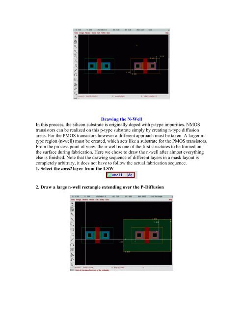
Drawing the N-Well<br />
In this process, the silicon substrate is originally doped with p-type impurities. NMOS<br />
transistors can be realized on this p-type substrate simply by creating n-type diffusion<br />
areas. For the PMOS transistors however a different approach must be taken: A larger n-<br />
type region (n-well) must be created, which acts like a substrate for the PMOS transistors.<br />
From the process point of view, the n-well is one of the first structures to be formed on<br />
the surface during fabrication. Here we chose to draw the n-well after almost everything<br />
else is finished. Note that the drawing sequence of different layers in a mask layout is<br />
completely arbitrary, it does not have to follow the actual fabrication sequence.<br />
1. Select the nwell layer from the LSW<br />
2. Draw a large n-well rectangle extending over the P-Diffusion