Tutorial 2 Inverter Layout
Tutorial 2 Inverter Layout
Tutorial 2 Inverter Layout

Create successful ePaper yourself
Turn your PDF publications into a flip-book with our unique Google optimized e-Paper software.
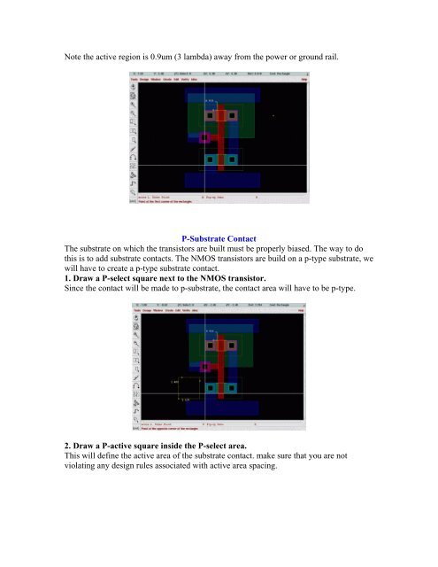
Note the active region is 0.9um (3 lambda) away from the power or ground rail.<br />
P-Substrate Contact<br />
The substrate on which the transistors are built must be properly biased. The way to do<br />
this is to add substrate contacts. The NMOS transistors are build on a p-type substrate, we<br />
will have to create a p-type substrate contact.<br />
1. Draw a P-select square next to the NMOS transistor.<br />
Since the contact will be made to p-substrate, the contact area will have to be p-type.<br />
2. Draw a P-active square inside the P-select area.<br />
This will define the active area of the substrate contact. make sure that you are not<br />
violating any design rules associated with active area spacing.