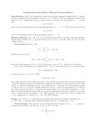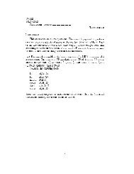
Tutorial 2 Inverter Layout
Tutorial 2 Inverter Layout
Tutorial 2 Inverter Layout

Create successful ePaper yourself
Turn your PDF publications into a flip-book with our unique Google optimized e-Paper software.
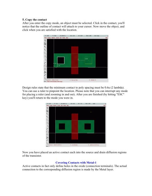
5. Copy the contact<br />
After you enter the copy mode, an object must be selected. Click in the contact, you'll<br />
notice that the outline of contact will attach to your cursor. Now move the object, and<br />
click when you are satisfied with the location.<br />
Design rules state that the minimum contact to poly spacing must be 0.6u (2 lambda).<br />
You can use a ruler to pinpoint the location. Please note that you can interrupt any mode<br />
for placing a ruler (and zooming in and out). After you are finished (by hitting "ESC"<br />
key) you'll return to the mode you were in.<br />
Now you have placed an active contact each into the source and drain diffusion regions<br />
of the transistor.<br />
Covering Contacts with Metal-1<br />
Active contacts in fact only define holes in the oxide (connection terminals). The actual<br />
connection to the corresponding diffusion region is made by the Metal layer.