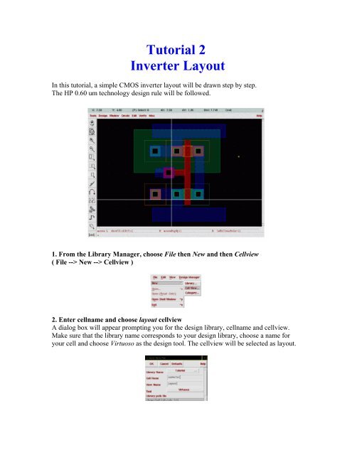
Tutorial 2 Inverter Layout
Tutorial 2 Inverter Layout
Tutorial 2 Inverter Layout

You also want an ePaper? Increase the reach of your titles
YUMPU automatically turns print PDFs into web optimized ePapers that Google loves.
<strong>Tutorial</strong> 2<br />
<strong>Inverter</strong> <strong>Layout</strong><br />
In this tutorial, a simple CMOS inverter layout will be drawn step by step.<br />
The HP 0.60 um technology design rule will be followed.<br />
1. From the Library Manager, choose File then New and then Cellview<br />
( File --> New --> Cellview )<br />
2. Enter cellname and choose layout cellview<br />
A dialog box will appear prompting you for the design library, cellname and cellview.<br />
Make sure that the library name corresponds to your design library, choose a name for<br />
your cell and choose Virtuoso as the design tool. The cellview will be selected as layout.
The LSW window and an empty Virtuoso will pop-up after you have entered the design<br />
name.<br />
LSW Window<br />
The Layer Selection Window (LSW) contains all the layers and their color formats<br />
that will be used to layout the circuitry.
nMOSFET <strong>Layout</strong><br />
Drawing the N-Diffusion (Active)<br />
We will start drawing the NMOS transistor. From the schematic, we know that this<br />
transistor size is W/L=1.2/0.6u. The width of the transistor will correspond to the width<br />
of the active area. We will select the n-diffusion layer and draw a rectangular active area<br />
to define the transistor.<br />
1. Select nactive layer from the LSW<br />
2. From the Create menu in Virtuoso select Rectangle<br />
(Create --> Rectangle )<br />
3. Draw the box<br />
You are now in rectangle mode. Select the first corner of rectangle in the layout window<br />
(you may select any point within the window but try to select a point close to the origin),<br />
click once, and then move the mouse cursor to the opposite corner. Using the information<br />
bar, draw a box that is 3.6u horizontal and 1.2u vertical. All units are in micrometers by<br />
default. To simplify the drawing, a grid of half a lambda is used, that is the cursor moves<br />
in 0.15u increments only. (Note, this number could be setup by click OptionsDisplay.<br />
In most cases, this number has been setup by the system, you may not need to change it).
3. It will be convenient if you have a ruler at hand.<br />
From the Window menu, click Create Ruler.<br />
The Gate Poly<br />
The second step is to draw the gate. We will use a vertical polysilicon rectangle to create<br />
the channel. Note that the length of the transistor channel will be determined by the width<br />
of this poly rectangle.<br />
1. Select poly layer from the LSW<br />
In our case we need to draw the poly rectangle in the middle of the diffusion region.<br />
3. Draw poly rectangle<br />
In our case we need to draw the poly rectangle in the middle of the diffusion region.<br />
Furthermore, according to design rules, poly must extend at least by 0.6u (2 Lambda)<br />
from the edge of the diffusion. Hence, the rectangle function is used to draw a poly<br />
rectangle that is 0.6u horizontal and 2.4u vertical.
Making Active Contacts<br />
The next step is to make the active contacts. These contacts will provide access to the<br />
drain and source regions of the NMOS transistor.<br />
1. Select the cc (Active Contact) layer from the LSW.<br />
2. Use the ruler to pinpoint a location 0.30u from the edges of diffusion.<br />
3. Create a square with a width and height of 0.6u within the active area.<br />
4. From the Edit menu choose Copy<br />
(Edit --> Copy)<br />
You could choose to draw the second contact the same way as you have drawn the first<br />
one. However, copying existing features is also a viable alternative.<br />
The copy dialog box will pop-up as soon as you select the copying mode. For this<br />
operation the default values are appropriate. The Snap Mode is an interesting option.<br />
When this is in orthogonal setting the copied objects will move only along one axis. This<br />
is a good feature to help you avoid alignment problems.
5. Copy the contact<br />
After you enter the copy mode, an object must be selected. Click in the contact, you'll<br />
notice that the outline of contact will attach to your cursor. Now move the object, and<br />
click when you are satisfied with the location.<br />
Design rules state that the minimum contact to poly spacing must be 0.6u (2 lambda).<br />
You can use a ruler to pinpoint the location. Please note that you can interrupt any mode<br />
for placing a ruler (and zooming in and out). After you are finished (by hitting "ESC"<br />
key) you'll return to the mode you were in.<br />
Now you have placed an active contact each into the source and drain diffusion regions<br />
of the transistor.<br />
Covering Contacts with Metal-1<br />
Active contacts in fact only define holes in the oxide (connection terminals). The actual<br />
connection to the corresponding diffusion region is made by the Metal layer.
1. Select layer Metal-1 from the LSW<br />
2. Draw two rectangles 1.2u wide to cover the contacts<br />
Note that Metal-1 has to extend over the contact in all directions by at least 0.3u (1<br />
lambda).<br />
The N-Select Layer<br />
Each diffusion area of each transistor must be selected as being of n-type or p-type. This<br />
is accomplished by a defining the "window: of n-type (or p-type) doping (implantation),<br />
through a special mask layer called n-select (p-select).<br />
1. Select nselect layer from the LSW.<br />
2. Draw a rectangle extending over the active area by 0.6u (2 lambda) in all<br />
directions.<br />
This is the complete layout process of a NMOS transistor.
PFET <strong>Layout</strong><br />
Drawing the P-Diffusion (Active)<br />
The next step is to draw the PMOS transistor. The basic steps involved in drawing the<br />
PMOS are the same.<br />
1. Select pactive layer from the LSW<br />
2. Draw a rectangle 3.6u by 1.2u<br />
You can use the cursor keys and the zoom function to find yourself a place to build the<br />
transistor. Make sure you leave enough separation between the NMOS and the PMOS.<br />
Note that the PMOS transistor will be surrounded by the N-well region.<br />
These three steps are identical to the ones done for the NMOS.<br />
1. Draw the gate poly<br />
2. Place the contacts
3. Cover contacts with Metal-1<br />
The P-Select Layer<br />
As with the NMOS transistor, the p-type doping (implantation) window over the active<br />
area must be defined using the n-pelect layer.<br />
1. Select pselect layer from the LSW<br />
2. Draw a rectangle that extends over the active area by 0.6u (2 lambda) in all<br />
directions.
Drawing the N-Well<br />
In this process, the silicon substrate is originally doped with p-type impurities. NMOS<br />
transistors can be realized on this p-type substrate simply by creating n-type diffusion<br />
areas. For the PMOS transistors however a different approach must be taken: A larger n-<br />
type region (n-well) must be created, which acts like a substrate for the PMOS transistors.<br />
From the process point of view, the n-well is one of the first structures to be formed on<br />
the surface during fabrication. Here we chose to draw the n-well after almost everything<br />
else is finished. Note that the drawing sequence of different layers in a mask layout is<br />
completely arbitrary, it does not have to follow the actual fabrication sequence.<br />
1. Select the nwell layer from the LSW<br />
2. Draw a large n-well rectangle extending over the P-Diffusion
The n-well must extend over the PMOS active area by a large margin, at least 1.8u (6<br />
lambda)<br />
Placing the PMOS and NMOS transistors<br />
Usually, in CMOS digital circuit design, it is desirable to place the PMOS transistor<br />
directly on top of the NMOS transistor for a compact layout.<br />
1. Select the PMOS transistor<br />
First make sure that you are in selection mode. If you are in any other mode (like<br />
rectangle drawing mode) exit the mode by pressing "ESC". Now using the mouse, click<br />
and drag a box that covers your PMOS. If you were successful, all the objects within the<br />
PMOS would be highlighted as in the figure below:<br />
2. From the menu Edit select the option Move<br />
( Edit --> Move )<br />
A window will pop-up similar to the copy window. This time we will have to change the<br />
Snap Mode option to Anyangle so that we can move the transistor freely.
3. Pick the reference point<br />
We will be asked to find a reference point for the object to be moved. The cursor will<br />
practically grab the object from that reference point. Since we want an accurate<br />
placement, it is advisable to select a point for which alignment is simpler. The corner<br />
between the diffusion and the poly is a good place to grab the PMOS.<br />
After we have picked the reference point, the outline of the shape will appear attached to<br />
the cursor and we will be able to move the shape around. Since the minimum distance<br />
from diffusion to the n-well edge is 1.8u, the PMOS and NMOS have to be at least 3.6u<br />
apart. We can place a ruler to help us aligning the two shapes and to measure the<br />
distance.<br />
Connecting the Output<br />
1. Draw a Metal-1 rectangle between NMOS and PMOS drain region contacts<br />
Note that the minimum Metal-1 width is 0.9u (3 lambda), thus narrower than the Metal-1<br />
covering the contacts. Also note that the transistors are completely symmetric, the source<br />
and drain regions are interchangeable.
4. Place the transistor<br />
You can drop the selected object (in this case consisting of the n-well, the p-active, poly<br />
and contacts) into its final location by clicking once on the left mouse button.<br />
Connecting the Input<br />
The next step will be to connect the gates of both transistors, which will form the input.<br />
To do this, we could use the rectangle command again, but this time we will use a<br />
different command, the path command. Throughout this tutorial, you will see that you<br />
typically have multiple options, commands or procedures available to create the same<br />
features in the layout. Please become familiar with as many of such options as possible.<br />
1. Select poly layer from the LSW<br />
2. From the Create menu select Path<br />
( Create --> Path )<br />
The path options box will pop up:<br />
In the path mode you can draw lines (or paths) with the selected layer. The width of the<br />
drawn line can be adjusted; the default is the minimum width of the selected layer.
3. Start path<br />
To start the path, click on the middle of the PMOS poly extension. You'll see a ghost line<br />
appear. Move this ghost line to the NMOS poly extension.<br />
4. Double click to finish path<br />
A single click will finish a line segment and let you continue drawing, a double click will<br />
finish the path.<br />
Making a Metal-1 connection for the Input<br />
In this design, we want that the layer for the input signal is Metal-1. Therefore we have to<br />
make a connection from the poly layer to the Metal-1 layer.<br />
This connection can be done manually by drawing a poly contact layer between Metal-1<br />
and poly, but we will use the path command to automatically add the contacts.
1. Starting from the poly line connecting the gates, start drawing a horizontal poly<br />
path<br />
2. On the Path Options dialog box, click on Change To Layer and switch to Metal1<br />
This will automatically add a contact to the end of the current path. Note that this will<br />
still be a ghost line. You can place the contact at a certain location by clicking once,<br />
thereafter the path will continue using the new layer.<br />
Power Rails<br />
Now that our transistors are placed and connected, we will have to add Power and<br />
Ground rails. Usually a layout consists of a large number of cells, all of which need<br />
power and ground connections. Therefore it is common to design cells such that they will<br />
have one continuous, wide power and ground connection when placed side by side.<br />
In this layout, the horizontal power and ground lines are drawn in Metal-1.<br />
1. Draw the Power Rail in Metal-1 above the PMOS<br />
2. Draw the Ground Rail in Metal-1 below the NMOS
Note the active region is 0.9um (3 lambda) away from the power or ground rail.<br />
P-Substrate Contact<br />
The substrate on which the transistors are built must be properly biased. The way to do<br />
this is to add substrate contacts. The NMOS transistors are build on a p-type substrate, we<br />
will have to create a p-type substrate contact.<br />
1. Draw a P-select square next to the NMOS transistor.<br />
Since the contact will be made to p-substrate, the contact area will have to be p-type.<br />
2. Draw a P-active square inside the P-select area.<br />
This will define the active area of the substrate contact. make sure that you are not<br />
violating any design rules associated with active area spacing.
3. Draw the active contact square inside the p-type active area.<br />
4. Make a metal connection to ground, covering the entire substrate contact.
Note that the susbtrate contact can also be created and placed as an instance, instead of<br />
drawing every item seperately. this alternative approach will be demonstrated in the next<br />
step, for the n-well contact.<br />
Make sure to connect the Power Rail and the Ground rail to the source contact of the<br />
PMOS and to that of NMOS, respectively.
N-Substrate Contact<br />
The PMOS transistor was placed within the n-well, this well also has to be biased with<br />
the VDD potential. This will be done with an n-type substrate contact.<br />
There are two ways to layout the substrate contact. One is to design every layer manually.<br />
The other way is to get the substrate contact instance from the library.<br />
1. From the menu Create select option Instance<br />
(Create --> Instance)<br />
This will pop-up the instance options menu.<br />
You'll have to provide a cell name and library here. It may be the case that you already<br />
know the cell name and cell view, but in this case it is better to Browse in your library to<br />
find the appropriate cell.<br />
NCSU_TechLib_hp06 ntap (Note, not NTAP)<br />
Using the same operation, to place the p-substrate contact ptap.<br />
2. Move the instance to the desired location.
3. Place the instance.<br />
Once satisfied, you can click to place the instance. You'll remain in the instance mode<br />
after you have placed the instance, press "ESC" to go back to selection mode again.<br />
4. Extend the N-Well to cover the N-Substrate contact.<br />
5. Make the Power connection<br />
Connect the N-substrate contact to Vdd, P-substrate contact to Gnd.
Design Rule Checking<br />
The layout must be drawn according to strict design rules. After you have finished your<br />
design, an automatic program will check each and every feature in your design against<br />
these design rules and report violations. This process is called Design Rule Checking<br />
(DRC).<br />
Our design is finished; we must now perform a Design rule Check to see if we have any<br />
errors.<br />
1. From the menu Verify select option DRC<br />
(Verify --> DRC )<br />
This will pop-up the DRC options dialog box.<br />
2. Start DRC<br />
The default options for the DRC are adequate for most situations. DRC results and<br />
progress will be displayed in the CIW. You'll have to check the results from the CIW.<br />
i