Raytheon Technology Today 2011 Issue 1
Raytheon Technology Today 2011 Issue 1
Raytheon Technology Today 2011 Issue 1

You also want an ePaper? Increase the reach of your titles
YUMPU automatically turns print PDFs into web optimized ePapers that Google loves.
The concept of a single atomic layer of<br />
crystalline material is easy enough to<br />
grasp, yet creating such a layer was<br />
not achieved until 2004, when two scientists,<br />
Andre Geim and Konstantin Novoslov,<br />
demonstrated the existence of a single<br />
atomic layer of carbon called graphene.<br />
This discovery was followed by a flurry of<br />
research activities, with the proposal of<br />
several applications for defense and commercial<br />
products. Through its support of<br />
several multidisciplinary research initiatives<br />
and DARPA-funded programs during the<br />
past three years, the U.S. Dept. of Defense<br />
has also indicated the importance of<br />
graphene for its military applications.<br />
The theoretically predicted and experimentally<br />
verified values of graphene properties<br />
have provided the impetus for a vast area<br />
of opportunity, from nano-scale devices to<br />
system-level advances. The implication of a<br />
single crystalline layer of pure carbon has<br />
spun many new startup businesses, which<br />
is likely to continue. Each is based on a<br />
unique finding aimed at anticipated and<br />
emerging markets. Among the technologies<br />
that can benefit from graphene in the near<br />
future are:<br />
Ultracapacitors. While batteries are high<br />
energy density power sources, they cannot<br />
deliver the energy to the load in short<br />
time, due to the natural process of ionic<br />
movement through an electrolyte between<br />
the battery electrodes. On the other hand,<br />
capacitors can release all their energy to<br />
the load in a very short time; however, they<br />
can store only a relatively small amount of<br />
energy. Replacement of the carbon charcoal<br />
with crumpled sheets of graphene<br />
provides several orders of magnitude higher<br />
charge storage capacity as in a battery,<br />
while allowing for faster charge/discharge<br />
time as in a capacitor — thus merging and<br />
improving the two power storage technologies.<br />
Ultracapacitor technology has<br />
the potential to significantly improve many<br />
<strong>Raytheon</strong> products such as radar front-end<br />
electronics, which we are considering as the<br />
first insertion point.<br />
Thermal management. In power electronics,<br />
heat removal from the active part of<br />
the device is a substantial challenge. The<br />
measured thermal conductivity (TC) of<br />
single layer graphene is reported to be<br />
nearly three times that of bulk diamond at<br />
55 W/cm-K. This is mainly attributed to the<br />
ability of phonons to propagate through the<br />
crystalline layer without suffering from any<br />
scattering processes. Engineering schemes<br />
need to be developed to exploit such high<br />
TC values successfully. Any method that<br />
can harvest the superior TC of graphene for<br />
thermal management in electronics circuitry<br />
can have extensive implications in all areas<br />
of digital, RF and optoelectronics.<br />
Transparent conductors. Due to its high<br />
sheet electronic charge density of 10 13 cm -2 ,<br />
and high electron mobility, graphene is a<br />
near perfect conductor. Furthermore, with<br />
its single atomic layer nature, graphene<br />
absorbs little visible light, making it an excellent<br />
transparent conductor. Commercial<br />
applications of this technology are already<br />
underway for use on touch-screen monitors,<br />
where large square-meter areas are being<br />
processed at one time. Such a low sheet<br />
resistance, low absorption layer is an ideal<br />
material for many <strong>Raytheon</strong> electro-optics<br />
applications, some of which currently<br />
use indium oxide. The same low sheet<br />
resistivity property of graphene can be<br />
exploited in interconnect technologies<br />
where material and fabrication cost<br />
can be a significant factor.<br />
THz Electronics. The superb material and<br />
electrical properties of this unique material<br />
system provide the potential for improved<br />
performance in the terahertz (THz) frequency<br />
range — performance that has been<br />
difficult to attain in conventional gallium<br />
arsenide (GaAs)- and gallium nitride (GaN)based<br />
material. A single atomic layer of<br />
crystalline carbon has been reported to have<br />
Special Interest<br />
Carbon-Based Electronic Devices Open a New Window<br />
to Electronics<br />
a room temperature electron mobility of<br />
greater than 200,000 cm 2 /(V-s), two and<br />
half times that of the best semiconductor.<br />
Such high electron mobility allows for ballistic<br />
electron transport in today’s transistors<br />
with state of the art geometries, hence<br />
making THz device fabrication highly feasible.<br />
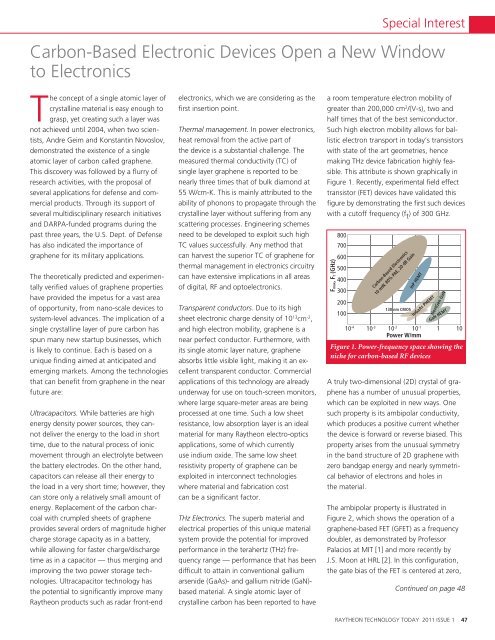
This attribute is shown graphically in<br />
Figure 1. Recently, experimental field effect<br />
transistor (FET) devices have validated this<br />
figure by demonstrating the first such devices<br />
with a cutoff frequency (f t ) of 300 GHz.<br />
Fmax, Ft (GHz)<br />
800<br />
700<br />
600<br />
500<br />
400<br />
300<br />
200<br />
100<br />
Carbon-Based Electronics<br />
10 mW, 80% PAE, 20 dB Gain<br />
130 nm CMOS<br />
InP HEMT<br />
InGaAs PHEMT<br />
NextGen GaN<br />
GaN HEMT<br />
10<br />
Power W/mm<br />
Figure 1. Power-frequency space showing the<br />
niche for carbon-based RF devices<br />
-4 10-3 10-2 10-1 1 10<br />
A truly two-dimensional (2D) crystal of graphene<br />
has a number of unusual properties,<br />
which can be exploited in new ways. One<br />
such property is its ambipolar conductivity,<br />
which produces a positive current whether<br />
the device is forward or reverse biased. This<br />
property arises from the unusual symmetry<br />
in the band structure of 2D graphene with<br />
zero bandgap energy and nearly symmetrical<br />
behavior of electrons and holes in<br />
the material.<br />
The ambipolar property is illustrated in<br />
Figure 2, which shows the operation of a<br />
graphene-based FET (GFET) as a frequency<br />
doubler, as demonstrated by Professor<br />
Palacios at MIT [1] and more recently by<br />
J.S. Moon at HRL [2]. In this configuration,<br />
the gate bias of the FET is centered at zero,<br />
Continued on page 48<br />
RAYTHEON TECHNOLOGY TODAY <strong>2011</strong> ISSUE 1 47