Impedance matching and Smith Chart : Basic Considerations
Impedance matching and Smith Chart : Basic Considerations
Impedance matching and Smith Chart : Basic Considerations
- No tags were found...

Create successful ePaper yourself
Turn your PDF publications into a flip-book with our unique Google optimized e-Paper software.
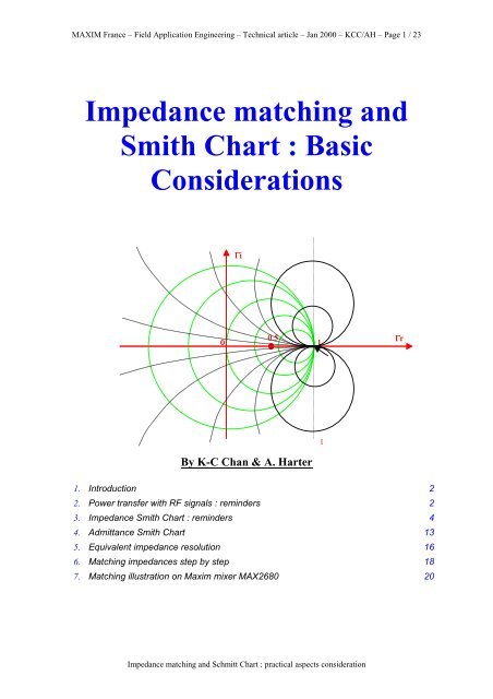
MAXIM France – Field Application Engineering – Technical article – Jan 2000 – KCC/AH – Page 1 / 23<strong>Impedance</strong> <strong>matching</strong> <strong>and</strong><strong>Smith</strong> <strong>Chart</strong> : <strong>Basic</strong><strong>Considerations</strong>Γi00.51Γr1By K-C Chan & A. Harter1. Introduction 22. Power transfer with RF signals : reminders 23. <strong>Impedance</strong> <strong>Smith</strong> <strong>Chart</strong> : reminders 44. Admittance <strong>Smith</strong> <strong>Chart</strong> 135. Equivalent impedance resolution 166. Matching impedances step by step 187. Matching illustration on Maxim mixer MAX2680 20<strong>Impedance</strong> <strong>matching</strong> <strong>and</strong> Schmitt <strong>Chart</strong> : practical aspects consideration
MAXIM France – Field Application Engineering – Technical article – Jan 2000 – KCC/AH – Page 2 / 231. Introductiona. When dealing with practical implementation of radio applications, there are alwayssome tasks that appear nightmare for many of us : need to match the differenceimpedances of the interconnected blocks : antenna to LNA, RFOUT to antenna, LNAoutput to mixer input, etc… The <strong>matching</strong> task is required mainly for a propertransfert of signal <strong>and</strong> energy from a "source" to a "load". The load can be then asource for a next block, etc…b. At high radio frequencies, the spurious (wires inductances, interlayers capacitances,conductors resistances, etc… are important non-predictible contributors for the<strong>matching</strong> network building. Above few tenth of MHz, theortical calculations <strong>and</strong>simulations are often not enough anymore. And in-situ RF lab measurements alongwith tuning work have to be considered for obtaining final correct values. Thecomputations values are required to set-up the type of the structure <strong>and</strong> targetcomponents values.c. There are many possible ways to "do impedance" <strong>matching</strong> :i. Computer simulations : complex to use since such simulators are dedicatedfor many stuffs <strong>and</strong> not only for impedance <strong>matching</strong> ! One has to befamiliarized with many input data to be entered on right formats <strong>and</strong> be expertto find the useful data among the tons of results coming out ! In addition, onehas to recognize that circuit simulators are usually not pre-installed on thenotebook.ii. Manual computations : tedious due to the length ("kilometric") of equations<strong>and</strong> the complex nature of the numbers to be manipulated.iii. Feelings : these can be acquired only one has already many years devotedonly for the RF domains. In short term, this is for super-specialist !iv. <strong>Smith</strong> <strong>Chart</strong>. This present article concentrates on the <strong>Smith</strong> <strong>Chart</strong> method : themain target here is to refresh its construction background <strong>and</strong> summarizepractical ways to use it by some practical illustration such as finding <strong>matching</strong>network components values. Of course <strong>matching</strong> for maximum power transferis not the only stuff one can do with <strong>Smith</strong> charts : optimization for best noisefigures, quality factors impact, stability analysis, etc,… can be effectivellycovered. These aspects will be h<strong>and</strong>led in an other arcticle (ref : AlphonseHarter).2. Power transfer with RF signals : remindersa. Before to efficiently introduce the <strong>Smith</strong> <strong>Chart</strong> utilities, it is recommended to have ashort refreshment on wave propagation phenomenons when Ics wires between ICs ona design are in RF conditions (above 100 MHz). This can be true at manycicumstancies such as in RS485 line, between a PA <strong>and</strong> an antenna, between a LNAto a donwconverter mixer, etc…b. Maximum power transferIt is well known that for getting a maximum power transfer from a source to a load,the following condition must happen :<strong>Impedance</strong> <strong>matching</strong> <strong>and</strong> Schmitt <strong>Chart</strong> : practical aspects consideration
MAXIM France – Field Application Engineering – Technical article – Jan 2000 – KCC/AH – Page 3 / 23Source impedance = complex conjugate of load impedance, or :R s + j.X s = R L – j.X LZsERsXsZLXLRLIn this condition, the energy transferred from the source to the load ismaximalized. In addition to an efficient power tranfer, this condition is required if onewants to avoid reflection of energy from the load back to the source; this isparticularly true for high frequency environments like video lines applications or RF& microwave networks.<strong>Impedance</strong> <strong>matching</strong> <strong>and</strong> Schmitt <strong>Chart</strong> : practical aspects consideration
MAXIM France – Field Application Engineering – Technical article – Jan 2000 – KCC/AH – Page 4 / 233. <strong>Impedance</strong> <strong>Smith</strong> <strong>Chart</strong> : remindersa. It appears as a circular plot with a lot of interlaced circles on it. It has been "invinted"by a certain Mr Phillip <strong>Smith</strong> at the Bell Lab in the 1930's. When correctly used,<strong>matching</strong> impedances with apparent complicate structures can be made without anycomputation. The only effort to do is to be able to read <strong>and</strong> follow values alongcircles.b. The <strong>Smith</strong> chart is a polar plot of the complex reflection coefficient (also calledgamma <strong>and</strong> symbolized by Γ), or more mathematically defined as : the 1- portscattering parameter s or s 11c. How is the <strong>Smith</strong> chart constructed ? We start from the load where the impedancemust be matched. Instead of considering its impedance directly, one expresses itsreflection coefficient Γ L . which is an other manner to characterize a load (such asadmittances, gain, transconductances, etc… The Γ L is more useful when dealing withRF frequencies.So : we know the reflection coefficient is defined as the ratio between the reflectedvoltage wave <strong>and</strong> the incident voltage wave :Z OVreflΓ L = VincVincVreflZ LThe amount of reflected signal from the load is depending on the degree of mismatchbetween the source impedance <strong>and</strong> the load impedance. Its expression has beendefined as follow :VreflΓ L = = VincZZLL− Z+ ZOO= Γ r + j. Γ I (equ 2.1)Since the impedances are complex numbers, the reflection coefficient is a complexnumber too.In order to reduce the number of unknown parameters, it is useful to freeze the onesthat appear often common in the application. Here Zo (the characteristic impedance) isoften a constant <strong>and</strong> a real industry normalized value : 50 Ω, 75 Ω, 100 Ω, 600 Ω,etc…We can then define a normalized load impedance :z = Z L /Zo = (R + jX) / Zo = r + jx (equ 2.2)With this simplification, we can rewrite the reflection coefficient formula :Γ L = Γ r + j.Γ i =ZZLL− Z+ ZOO=( Z( ZLL− Z+ ZOO) / Z) / ZOO=z −1=z + 1r +r +j.x −1j.x + 1(equ 2.3)Here one can see the direct relationship between load impedance <strong>and</strong> itsreflection coefficient. Unfortunnally the complex nature of the relation is notpractically useful. The <strong>Smith</strong> chart is a kind of graphical representation of the<strong>Impedance</strong> <strong>matching</strong> <strong>and</strong> Schmitt <strong>Chart</strong> : practical aspects consideration
MAXIM France – Field Application Engineering – Technical article – Jan 2000 – KCC/AH – Page 5 / 23above equation. In order to build the chart, the equation must be re-written inorder to extract st<strong>and</strong>ard geometrical figures (likes circles or stray lines).By reversing the (equ 2.3) :z = r +1+ Γjx =1− ΓLL2r2r1+ Γ=1− Γrr+ jΓi− jΓi2ii(equ 2.4)2(1 + Γr+ jΓi).(1 − Γr+ jΓi) 1− Γ − Γi+ j.2.Γr + jx ==(equ 2.5)(1 − Γ − jΓ).(1 − Γ + jΓ) 1+ Γ − 2. Γ + ΓrirBy equalling the real parts <strong>and</strong> the imaginary parts of (equ 2.5) we obtain 2independent new relations :ir2 21− Γr− Γir = (equ 2.6)1+ Γ − 2. Γ + Γ2rr2i2. Γix = (equ 2.7)1+ Γ − 2. Γ + Γ2rr2iBy developing (equ 2.6) :2r + r Γ − 2. r.Γ2+ r.Γ2 2= 1− Γ − Γ(equ 2.8).rr ir i2 22 2Γ + r.Γ − 2. r.Γ + r.Γ + Γ = 1−rrrr22(1 + r).Γ − 2. r.Γ + ( r + 1). Γ = 1−rΓΓ2r2rrr2.r2. Γr+ Γi−r + 12. r− . Γr + 1r1−r=1+r2r+ + Γ2 i( r + 1)i2ii2r−( r + 1)2(equ 2.9)(equ 2.10)(equ 2.11)1−r= (equ 2.12)1+r(rr + 11−r1+rr(1 + r)1(1 + r)22 2Γr− ) + Γi= + =22(equ 2.13)(rr + 111+rParametric equation of the type (x-a)² + (y+b)²=R²2 22Γr− ) + Γi= ( )(equ 2.14)<strong>Impedance</strong> <strong>matching</strong> <strong>and</strong> Schmitt <strong>Chart</strong> : practical aspects consideration
MAXIM France – Field Application Engineering – Technical article – Jan 2000 – KCC/AH – Page 6 / 23This above relation is a parametric equation, in the complex plan (Γr,Γi), of a circle centred atcoordinate (r/r+1 , 0) <strong>and</strong> having a radius of 1/(1+r).r =0 (short)Γir =1The points situated on a circle are all the impedancescharacterized by a same real impedance part value.For example, the circle R=1 is centred at coordinate(0.5;0) <strong>and</strong> having a radius of 0.5. It include the point(0,0) which is the reflection zero point (the load ismatched with the characteristic impedance). A shortcircuitas load gives according to the formula a circlecentred at coordinate (0.0) <strong>and</strong> having a radius of 1.00.51Γrr =∞(open)For a open-circuit load, the circle is degenerated asa single point (circle centred at coordinate 1,0 <strong>and</strong>having a radius of 0) : this correspond to amaximum reflection coefficient of 1 : all theincident wave is totally reflected)Some particular cases to be noticed :• All the circles have one unique same intersecting point at the coordinate (1,0)• The 0 ohms circle (r=0; no resistive part) is the biggest one• The infinite resistor circle is reduced to one point at (1,0)• There is no negative resistors (if r
MAXIM France – Field Application Engineering – Technical article – Jan 2000 – KCC/AH – Page 7 / 23This above relation is a parametric equation, in the complex plan (Γr,Γi), of a circle centred atcoordinate (1 , 1/x) <strong>and</strong> having a radius of 1/x.ΓiThe points situated on a circle areall the impedances characterizedby a same imaginary impedancepart value x. For example, thecircle x=1 is centred at coordinate(1;1) <strong>and</strong> having a radius of 1. Allcircles (constant x) include thepoint (1,0)00.51ΓrIn difference with the real part circles,x can be positive or negative : thisexplain the duplicate mirror circles atthe bottom side of the complex plan.All the circles centres are placed onthe vertical axe intersecting the point1.1• Some particularities to be noticed :• The zero-reactance circle (thus a pure resistive load) is just the horizontal axis of thecomplex plane.• The infinite reactance is a degenerated circle to one point situated at (1,0).• All constant reactance circles have the same unique intersecting point at (1,0)• Positive reactance’s (inductors) are on circles on the half upper part of the chart, whilenegative reactance’s (capacitors) are on the half bottom part of the chart• Changing a reactance is just then to take an other circle of the family corresponding to thenew value x.<strong>Impedance</strong> <strong>matching</strong> <strong>and</strong> Schmitt <strong>Chart</strong> : practical aspects consideration
MAXIM France – Field Application Engineering – Technical article – Jan 2000 – KCC/AH – Page 8 / 23Now, to complete our <strong>Smith</strong> <strong>Chart</strong>, we superpose the 2 circles families <strong>and</strong> one can see thatevery circle of a family does intersect ALL the circles of the other family. Thus knowing theimpedance in the for of r + jx, the plot gives immediately the corresponding reflection coefficient : onehas only to find the intersection point of 2 circles : one circle corresponding to the value r <strong>and</strong> onecircle corresponding to value x. The opposite operation is also trivial : knowing the reflectioncoefficient, find the 2 circles passing both on that point <strong>and</strong> read the values r <strong>and</strong> x corresponding tothe found circles.Γi00.51Γr1Now we can do following tasks (the list is not complete) :• Situate any impedance as a spot on the <strong>Smith</strong> <strong>Chart</strong>• Find the reflection coefficient Γ for a given impedance (<strong>and</strong> knowing the characteristicimpedance)• Find the impedance when knowing Γ• Convert impedance to admittance <strong>and</strong> vice-versa• Find equivalent impedance• Find components values for a wanted reflection coefficient (in particular find elements of a<strong>matching</strong> network)<strong>Impedance</strong> <strong>matching</strong> <strong>and</strong> Schmitt <strong>Chart</strong> : practical aspects consideration
MAXIM France – Field Application Engineering – Technical article – Jan 2000 – KCC/AH – Page 9 / 23Since the <strong>Smith</strong> <strong>Chart</strong> resolution technique is basically a graphic method, the precision of the solutionsdepends a lot on the graph definitions. Here below we joined a typical <strong>Smith</strong> <strong>Chart</strong> used by all the RFengineers :<strong>Impedance</strong> <strong>matching</strong> <strong>and</strong> Schmitt <strong>Chart</strong> : practical aspects consideration
MAXIM France – Field Application Engineering – Technical article – Jan 2000 – KCC/AH – Page 10 / 23• Example 1 : situate on the <strong>Smith</strong> chart <strong>and</strong> by considering a characteristic impedance of 50ohms, the here below listed impedances.Z 1 = 100 + j50 ohms Z 2 = 75 –j100 ohms Z 3 = j200 ohms Z 4 = 150 ohmsZ 5 = open-circuit Z 6 = short-circuit Z 7 = 50 ohms Z 8 = 184 –j900 ohmsFirst thing to do : normalize first the impedance (division by the characterise impedance) :z 1 = 2 + j z 2 = 1.5 –j2 z 3 = j4 z 4 = 3z 5 = ∞ z 6 = 0 z 7 = 1 z 8 = 3.68 –j18<strong>Impedance</strong> <strong>matching</strong> <strong>and</strong> Schmitt <strong>Chart</strong> : practical aspects consideration
MAXIM France – Field Application Engineering – Technical article – Jan 2000 – KCC/AH – Page 11 / 23• Example 2 : Direct extraction of reflection coefficient Γ on the <strong>Smith</strong> <strong>Chart</strong>.Solution : Once the impedance point well situated on the plot (intersection point of a constantresistor circle <strong>and</strong> of a constant reactance circle), just read the rectangular coordinates :projection on the horizontal axis will give Γ r (real part of the reflection coefficient) <strong>and</strong> theprojection on the vertical axis will give Γ i (imaginary part of the reflection coefficient).Γ iConstantresistor rConstantreactance xΓ r0 1• Example 3 : Take the 8 cases h<strong>and</strong>led in example 1 <strong>and</strong> extract their corresponding Γ directlyon the <strong>Smith</strong> <strong>Chart</strong>.Γ 1 = 0.4 + 0.2j Γ 2 = 0.51 - 0.4j Γ 3 = 0.875 + 0.48j Γ 4 = 0.5Γ 5 = 1 Γ 6 = -1 Γ 7 = 0 Γ 8 = 0.96 - 0.1j<strong>Impedance</strong> <strong>matching</strong> <strong>and</strong> Schmitt <strong>Chart</strong> : practical aspects consideration
MAXIM France – Field Application Engineering – Technical article – Jan 2000 – KCC/AH – Page 12 / 23Working with admittanceThe <strong>Smith</strong> <strong>Chart</strong> is built by considering impedance (resistor <strong>and</strong> reactance). Adding elementsin series are trivial : they correspond to moves along circles. Unfortunally, summing elementsin parallel needs some additional consideration in the <strong>Smith</strong> <strong>Chart</strong>.We know that by definition, Y = 1/Z <strong>and</strong> Z = 1/Y. The admittance is expressed in Mho or Ω -1(in the older time as Siemens or S). Of course, since Z is complex, Y is also complex.Y = G + j.B where G is called “conductance” <strong>and</strong> B the “susceptance” of the element.One has not to conclude that G=1/R <strong>and</strong> B=1/X !!! which are wrong !By normalising by y = Y/Yo :y = g + j.bWhat happen with the reflection coefficient ?Γ =ZZLL− Z+ ZOO1 Y=1 YLL−1Y+ 1 YOOY=YOO− YL+ YL1−=1+yyOne can see the expression for Γ is opposite in sign compared to its expression with z :Γ(y) = -Γ(z)Thus, if we know z, by inverting the signs of Γ, we found a point situated at the same distanceto (0,0) but in the opposite direction. The same result can be obtained by making a rotation of180° angle around the centre point.zΓiConstantconductance gcircle180°Γr-ΓrConstancesusceptanceb circle-ΓiyOf course, while Z <strong>and</strong> 1/Z do represent exactly a same component, the new point appears as acomplete different impedance (different point in the <strong>Smith</strong> chart, different reflection value,etc…). That is because the plot is an impedance plot <strong>and</strong> the new point is in fact anadmittance. The value read on the chart has then to be read as mho.This method is OK for making conversion, but not enough to make circuit resolution whendealing with elements in parallel.<strong>Impedance</strong> <strong>matching</strong> <strong>and</strong> Schmitt <strong>Chart</strong> : practical aspects consideration
MAXIM France – Field Application Engineering – Technical article – Jan 2000 – KCC/AH – Page 13 / 234. Admittance <strong>Smith</strong> <strong>Chart</strong>Above, we have seen that every point in the impedance <strong>Smith</strong> <strong>Chart</strong> can be converted into anadmittance counterpart by making a rotation of 180° around the origin of the Γ complex plane.Thus, an Admittance <strong>Smith</strong> <strong>Chart</strong> can be obtained by rotating the whole <strong>Impedance</strong> <strong>Smith</strong><strong>Chart</strong> by 180°. This is great since one has not to build an other chart : the same can be used !Automatically, the intersecting point of all the circles (constant conductance’s <strong>and</strong> constantsusceptances) is at the point (-1, 0). With that plot, adding element in parallel becomes trivial.One can also mathematically demonstrate the Admittance <strong>Smith</strong> chart construction :1− y 1−g − jbΓ L = Γ r + j.Γ i = = =(equ 3.1)1 + y 1+g + jbBy reversing the (equ 3.1) :y = g +1− Γjb =1+ ΓLL2r2r1− Γ=1+ Γrr− jΓi+ jΓi2ii(equ 3.2)2(1 − Γr− jΓi).(1 + Γr− jΓi) 1− Γ − Γi− j.2.Γg + jb ==(equ 3.3)(1 + Γ + jΓ).(1 + Γ − jΓ) 1+ Γ + 2. Γ + ΓrirBy equalling the real parts <strong>and</strong> the imaginary parts of (equ 3.3) we obtain 2independent new relations :ir2 21− Γr− Γig = (equ 3.4)1+ Γ + 2. Γ + Γ2rr2i− 2. Γib = (equ 3.5)1+ Γ + 2. Γ + Γ2rr2iBy developing (equ 3.4) :222 2g + g. Γr+ 2. g.Γr+ g.Γi= 1− Γr− Γi(equ 3.6)2 22 2Γr+ g.Γr+ 2. g.Γr+ g.Γi+ Γi= 1−g(equ 3.7)22(1 + g).Γr+ 2. g.Γr+ ( g + 1). Γi= 1−g(equ 3.8)2 2.g2 1−gΓr+ . Γr+ Γi=g + 1 1+g(equ 3.9)222 2. g g2 g 1−gΓr+ . Γr+ + Γi− =22g + 1 ( g + 1) ( g + 1) 1+g(equ 3.10)(gg + 11−g1+gg(1 + g)1(1 + g)22 2Γr+ ) + Γi= + =22(equ 3.11)(gg + 111+gParametric equation of the type (x-a)² + (y+b)²=R²2 22Γr+ ) + Γi= ( )(equ 3.12)<strong>Impedance</strong> <strong>matching</strong> <strong>and</strong> Schmitt <strong>Chart</strong> : practical aspects consideration
MAXIM France – Field Application Engineering – Technical article – Jan 2000 – KCC/AH – Page 14 / 23g =∞(short)This above relation is a parametric equation, in the complex plan (Γr,Γi), of a circle centred atcoordinate (-g/g+1 , 0) <strong>and</strong> having a radius of 1/(1+g).g =0 (open)-1 0ΓiThe points situated on a circle are all the admittancescharacterized by a same real part (conductance)value. For example, the circle g=1 is centered atcoordinate (-0.5;0) <strong>and</strong> having a radius of 0.5. Itinclude the point (0,0) which is the reflection zeropoint (the load is matched with the characteristicadmittance). An open-circuit as load gives accordingto the formula a circle centred at coordinate (0.0) <strong>and</strong>having a radius of 1.ΓrFor a short-circuit load, the circle is degenerated asa single point (circle centred at coordinate -1,0 <strong>and</strong>having a radius of 0) : this corresponds to amaximum reflection coefficient of -1 : all theincident wave is totally reflected)<strong>Impedance</strong> <strong>matching</strong> <strong>and</strong> Schmitt <strong>Chart</strong> : practical aspects consideration
MAXIM France – Field Application Engineering – Technical article – Jan 2000 – KCC/AH – Page 15 / 23By developing (equ 3.5) :2b + b.Γ + 2. b.Γ2+ b.Γ = −2.Γrrii(equ 3.13)221+ Γ + 2. Γ + . Γ = −2.Γ b(equ 3.14)r r ii/22 2Γr+ 2. Γr+ 1+ Γi+ Γi= 0(equ 3.15)b22 2 1 1Γ + 2.Γ + 1+ Γ + Γ + − = 0(equ 3.16)r ri2 2bib b2 1 2 1( Γr+ 1) + ( Γi+ ) =2(equ 3.17)b bAgain, this is also a parametric equation of the type (x-a)² + (y+b)²=R²This above relation is a parametric equation, in the complex plan (Γr,Γi), of a circle centred atcoordinate (-1 , -1/b) <strong>and</strong> having a radius of 1/b.-1Γi0The points situated on a circleare all the admittancescharacterized by a sameimaginary part value b. Forexample, the circle b=1 iscentred at coordinate (-1;-1)<strong>and</strong> having a radius of 1. Allcircles (constant b) include thepoint (-1,0)Γr<strong>Impedance</strong> <strong>matching</strong> <strong>and</strong> Schmitt <strong>Chart</strong> : practical aspects consideration
MAXIM France – Field Application Engineering – Technical article – Jan 2000 – KCC/AH – Page 16 / 235. Equivalent impedance resolutionWhen solving problem where elements in series <strong>and</strong> in parallel are mixed together, one canuse the same <strong>Smith</strong> <strong>Chart</strong> <strong>and</strong> rotate it at any instant when conversions from z to y or y to z arepreviously performed before to rotate the chart.The best way to expose the method is to do this through an example :Let’s consider the network here below (the elements are normalized with Zo=50 ohm):Serie reactance (x) is positive for inductance <strong>and</strong> negative for capacitor. While susceptance (b)is positive for capacitance <strong>and</strong> negative for inductance.x = 0.9 x = -1.4 x = 1Z = ?b = 1.1b = -0.3r = 1The circuit has to be cut in different portions such as :x = 0.9b = 1.1x = -1.4b = -0.3x = 1r = 1Z = ?AZDCB• Step 1 : We start from the end, which is here a resistor of 1. Since this is in series with aninductor of 1 ohm, the spot on the <strong>Smith</strong> chart comes immediately : intersection circle r=1 <strong>and</strong>circle x=1. We mark this point by A• Step 2 : The next element is an element coming in shunt (parallel) : we will have to switch intothe Admittance <strong>Smith</strong> <strong>Chart</strong> (rotation by 180° of the whole plane). Before to do this rotation,first, convert the previous point into admittance : this gives the spot A’.• Step 3 : Rotate the plane by 180° : we are now in the admittance mode. The shunt element canbe added by going along the conductance circle by a distance corresponding to 0.3. This has tobe made in the anti-clock wise direction (negative value). After doing this, we obtain point B.• Step 4 : We have an element to be inserted in series. This means we need to switch to theimpedance <strong>Smith</strong> <strong>Chart</strong>. Before to do this, reconvert the previous point into impedance (it wasan admittance). This gives the spot B’.• Step 5 : Rotate the plane by 180° : we are now in the impedance mode. The series element isadded by circulating along the resistance circle by a distance corresponding to 1.4. This has tobe made in the anti-clock wise direction (negative value). After doing this, we obtain point C.<strong>Impedance</strong> <strong>matching</strong> <strong>and</strong> Schmitt <strong>Chart</strong> : practical aspects consideration
MAXIM France – Field Application Engineering – Technical article – Jan 2000 – KCC/AH – Page 17 / 23• Step 6 : Again, there is a shunt element, same operations as already described above(conversion into admittance followed by plane rotation of 180°. Then apply move by distance1.1 in the clock-wise direction, since the value is positive, along the constant conductancecircle). We obtain point D.• Step 7 : Recon version into impedance prior to add the last element (series inductor). Weobtain the asked value : z situated in the intersection of circle resistor 0.2 <strong>and</strong> circle reactance0.5 : thus z = 0.2 +j0.5. If the system characteristic impedance is 50 ohms, then Z = 10 + j25ohms<strong>Impedance</strong> <strong>matching</strong> <strong>and</strong> Schmitt <strong>Chart</strong> : practical aspects consideration
MAXIM France – Field Application Engineering – Technical article – Jan 2000 – KCC/AH – Page 18 / 236. Matching impedances step by stepThis is the reverse operation of finding equivalent impedance of a given network. Here, theimpedances are fixed at the 2 access ends (often the source <strong>and</strong> the load). The task is to designthe network to be inserted between them in order to insure impedance <strong>matching</strong>. Apparently, itlooks like as easy as finding equivalent impedance, but the problem is that there may existsinfinite ways (i.e. <strong>matching</strong> networks) to realize a same <strong>matching</strong>. Other inputs can beprovided or fixed : filter type structure, quality factor, limited choice of element values, etc…The approach is to add series <strong>and</strong> shunt elements on the chart until the desired impedance isachieved. Graphically, it appears to find the way to link 2 spots on the <strong>Smith</strong> <strong>Chart</strong>.The best method to explain the approach is to illustrate the tasks with the help of a practicalexample :Matching networkZ S = 25 - j15 ΩVsZ * =25 + j15 ΩL = ?C = ?Z L = 100 – j25 ΩHere the problem consists to match a source impedance Zs to a ZL load at the operationfrequency of 60 MHz. The network structure has been fixed as a low pass L type.An other manner to see the problem is to say how to force the load to appear like animpedance of value = Zs * (complex conjugate of Zs).Step 1 : First normalize the different impedance values. If not given, choose the value in thesame range than load/source values (question of readability on the <strong>Smith</strong> chart). Here we takeZo = 50 ohmsThus zs = 0.5 – j0.3 <strong>and</strong> z * s = 0.5 + j0.3zL = 2 – j0.5Step 2 : Situate the 2 points on the chart. We mark A for zL <strong>and</strong> D for Z*.Step 3 : The first element connected to the load is a capacitor in shunt : conversion inadmittance (see previously described methodology). We obtain a point A’.Step 4 : Detect the arc portion that the next point will appear after the connection of thecapacitor C. Since we don’t know the value of C, we don’t know where to stop. We know thedirection (C in shunt means in the clock-wise direction in the admittance <strong>Smith</strong> chart). Thepoint B will be an admittance.Since the next element is a series element, the point B has to be back converted in impedance.Thus a point B’ will be obtained. This point B’ has to be situated in the same resistor circlethan D. Graphically, there is only one solution from A’ to D but the intermediate point B (<strong>and</strong>hence B’) needs to be localized by “test-<strong>and</strong>-try” until one falls on the point D.<strong>Impedance</strong> <strong>matching</strong> <strong>and</strong> Schmitt <strong>Chart</strong> : practical aspects consideration
MAXIM France – Field Application Engineering – Technical article – Jan 2000 – KCC/AH – Page 19 / 23Step 5 : after having found the points B, B’, we can then measure the lengths of arc A’-B <strong>and</strong>arc B’-D. The first gives the normalised susceptance value of C <strong>and</strong> the second gives thenormalised reactance value of L.After apprx 15 minutes , one found the points B <strong>and</strong> B’ :The arc A’-B measures b = 0.78 <strong>and</strong> thus B = 0.78 * Yo = 0.0156 mhoSince ω.C = B, then C = B/ω = B/(2.π.f) = 0.0156/(2.π.60.10 6 ) = 41.4 pFThe arc B’-D measures x = 1.2 <strong>and</strong> thus X = 1.2 * Zo = 60 ohmSince ω.L = X, then L = X/ω = X/(2.π.f) = 60/(2.π.60.10 6 ) = 159 nH<strong>Impedance</strong> <strong>matching</strong> <strong>and</strong> Schmitt <strong>Chart</strong> : practical aspects consideration
MAXIM France – Field Application Engineering – Technical article – Jan 2000 – KCC/AH – Page 20 / 237. <strong>Impedance</strong> <strong>matching</strong> illustration on Maxim mixer MAX2680Practical application on MAX2680-MAC2681-MAX2682 which are down converters mixersable to h<strong>and</strong>le input RF signal on the range 400MHz to 2.5GHz into output IF frequenciesfrom 10 MHz to 500 MHz. The external <strong>matching</strong> networks on the RF input <strong>and</strong> IF outputports determine their operation modes. Their structures <strong>and</strong> elements are various <strong>and</strong> quasiinfinite. The applications nature (i.e. Q-factor, needs to pass or filter out DC, range limits ofcomponents, etc…) will fix the best choices.In their datasheet, a typical <strong>matching</strong> structure has been proposed with elements values forsome “st<strong>and</strong>ardized” frequencies :• Input RF at 400 MHz, 900 MHz, 1950 MHz <strong>and</strong> 2450 MHz• Output RF at 45 MHz, 70 MHz <strong>and</strong> 240 MHzThe question many of us are asking or will ask is : how to proceed if the application used otherfrequencies ?The above highlights on impedance <strong>matching</strong> will help us to h<strong>and</strong>le the issue :Let us first consider the proposed IF output <strong>matching</strong> network :ZsC2MAX2680MAX2681MAX2682L1R1LoadZL50 ΩIF MatchingnetworkZs is the IF output stage internal impedance (Thevenin equivalent) that needs to be matchedwith the external line of 50 Ω. The Zs has been given for the 3 different devices <strong>and</strong> for the 3st<strong>and</strong>ard IF frequencies :Zs IF = 45 MHz IF = 70 MHz IF = 240 MHzMAX2680 960-j372 803-j785 186-j397MAX2681 934-j373 746-j526 161-j375MAX2682 670-j216 578-j299 175-j296The datasheet contains a table with elements values for the same above defined 3 st<strong>and</strong>ard IFfrequencies :IF Matching IF = 45 MHz IF = 70 MHz IF = 240 MHzL1 390 nH 330 nH 82 nHC2 39 pF 15 pF 3 pFR1 250 Ω Open openLet us verify on the <strong>Smith</strong> chart the data for the MAX2680 at IF = 240 MHz.• First step : Choose the characteristic impedance : here Zo = 50 Ω, compute thenormalized values zL <strong>and</strong> zs*. Here we have zL = 1 <strong>and</strong> zs* = 3.72 + j7.94• Step 2 : Plot the zL <strong>and</strong> zS* on the chart<strong>Impedance</strong> <strong>matching</strong> <strong>and</strong> Schmitt <strong>Chart</strong> : practical aspects consideration
MAXIM France – Field Application Engineering – Technical article – Jan 2000 – KCC/AH – Page 21 / 23• Step 3 : Start from zL, turn anti-clock wise (because capacitor in series thus negativereactance) of a quantity still to be determined. The end point must be situated on theconstant r=1 circle in a such way that the L1 shunt (anti-clock wise rotation in theadmittance chart) will end to zs*. Optionally, shunt R1 must be added if theintermediate point is to far for reaching zs*.The operations are illustrated in the following <strong>Smith</strong> <strong>Chart</strong>.<strong>Impedance</strong> <strong>matching</strong> <strong>and</strong> Schmitt <strong>Chart</strong> : practical aspects consideration
MAXIM France – Field Application Engineering – Technical article – Jan 2000 – KCC/AH – Page 22 / 23The arc A-B gives the value of the capacitor C2The arc C-D gives the value of the inductor L1It is not necessary to add the shunt resistor R1 in this case.Value of arc A-B measured on the plot : r = 4.5 units, thus Z = 50 * 4.5 = 225 ohmsThus C 2 = 1/(225*ω) = 1/(225*2*π*f) = 1 / (225*2*π*240 10 6 ) = 2.94 pFValue of arc C-D measured on the plot : s = 0.3 units, thus Z = 50/0.3 = 167 ohmsThus L 1 = 167 / ω = 167 / (2*π*f) = 167 / (2*π*240 10 6 ) = 110 nHThe same manipulations for MAX2681 give same results since the impedance is quasiidentical.For the MAX2682, an identical set of operations on the <strong>Smith</strong> <strong>Chart</strong> give 3.7 for the arc BC<strong>and</strong> 0.37 for the arc CD. These results for C 2 = 3.6 pF <strong>and</strong> L 1 =89 nHValues are thus very close for a same IF frequency on the 3 products MAX2680, MAX2681<strong>and</strong> MAX2682At IF = 70 MHz, the arc lengths AB <strong>and</strong> CD are very close to the cases at IF = 240 MHz, theseend then with C 2 = 12 pF <strong>and</strong> L 1 value is 310 nHAt IF = 45 MHz, the shunt resistor is required if we want to avoid too big inductance. The“price” to pay is a little bit a degradation of the Q factor. The shunt resistor allows a decreasein constant g circle in the Admittance <strong>Smith</strong> chart. One can observe both the AB <strong>and</strong> the CDarcs are shorter than the situation without the shunt. After the manipulation on the chart, onecan measure arc AB = 1.65 (resulting in a 42 pF value for C2) <strong>and</strong> arc CD = 0.5 (resulting onan inductor value L1 of 351 nH). The case at 45 MHz is illustrated in the hereafter <strong>Smith</strong><strong>Chart</strong>.After having placed the Zs <strong>and</strong> the Z L spots on the chart, start from Z L (point A : r=1, x=0) <strong>and</strong>we know the first element is a series capacitor : thus next point is B situated somewhere on thecircle r=1. The point B transformed into admittance must give a point C situated 180° phase.As explained above, it will be added a shunt resistor : converted into conductance, itcorresponds to subtract a value. We choose (apprx) 250 ohms (0.2 mho normalizedconductance). It is a shift of point C into D along a constant susceptance circle starting from C.One D is obtained, its recon version into impedance must fall into Zs (point E).We measure arc AB : 1.65 meaning 82.5 ohms at 45 MHz <strong>and</strong> giving C 2 = 42 pFWe measure then arc CD : 0.45 meaning 111.1 ohms at 45 MHz <strong>and</strong> giving L 1 = 390 nHBy considering also the need to use st<strong>and</strong>ardized components values, one find the data givenin the datasheet.<strong>Impedance</strong> <strong>matching</strong> <strong>and</strong> Schmitt <strong>Chart</strong> : practical aspects consideration
MAXIM France – Field Application Engineering – Technical article – Jan 2000 – KCC/AH – Page 23 / 23<strong>Impedance</strong> <strong>matching</strong> <strong>and</strong> Schmitt <strong>Chart</strong> : practical aspects consideration