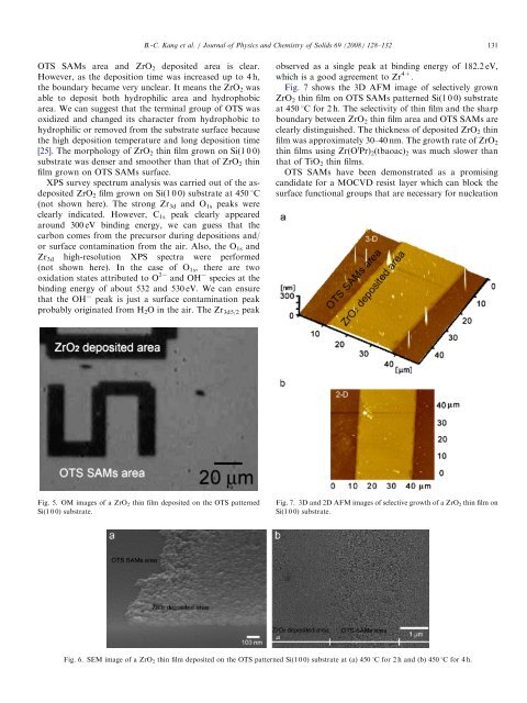
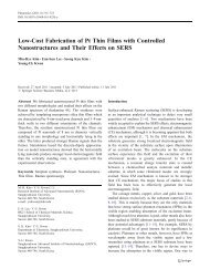
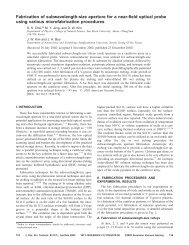
ARTICLE IN PRESSB.-C. Kang et al. / Journal <strong>of</strong> Physics <strong>and</strong> Chemistry <strong>of</strong> Solids 69 (2008) 128–132 131OTS SAMs area <strong>and</strong> ZrO 2 deposited area is clear.However, as the deposition time was increased up to 4 h,the boundary became very unclear. It means the ZrO 2 wasable to deposit both hydrophilic area <strong>and</strong> hydrophobicarea. We can suggest that the terminal group <strong>of</strong> OTS wasoxidized <strong>and</strong> changed its character from hydrophobic tohydrophilic or removed from the substrate surface becausethe high deposition temperature <strong>and</strong> long deposition time[25]. The morphology <strong>of</strong> ZrO 2 <strong>thin</strong> film grown on Si(1 0 0)substrate was denser <strong>and</strong> smoother than that <strong>of</strong> ZrO 2 <strong>thin</strong>film grown on OTS SAMs surface.XPS survey spectrum analysis was carried out <strong>of</strong> the asdepositedZrO 2 film grown on Si(1 0 0) substrate at 450 1C(not shown here). The strong Zr 3d <strong>and</strong> O 1s peaks wereclearly indicated. However, C 1s peak clearly appearedaround 300 eV binding energy, we can guess that thecarbon comes from the precursor during depositions <strong>and</strong>/or surface contamination from the air. Also, the O 1s <strong>and</strong>Zr 3d high-resolution XPS spectra were performed(not shown here). In the case <strong>of</strong> O 1s , there are twooxidation states attributed to O 2 <strong>and</strong> OH species at thebinding energy <strong>of</strong> about 532 <strong>and</strong> 530 eV. We can ensurethat the OH peak is just a surface contamination peakprobably originated from H 2 O in the air. The Zr 3d5/2 peakobserved as a single peak at binding energy <strong>of</strong> 182.2 eV,which is a good agreement to Zr 4+ .Fig. 7 shows the 3D AFM image <strong>of</strong> selectively grownZrO 2 <strong>thin</strong> film on OTS SAMs patterned Si(1 0 0) substrateat 450 1C for 2 h. The selectivity <strong>of</strong> <strong>thin</strong> film <strong>and</strong> the sharpboundary between ZrO 2 <strong>thin</strong> film area <strong>and</strong> OTS SAMs areclearly distinguished. The thickness <strong>of</strong> deposited ZrO 2 <strong>thin</strong>film was approximately 30–40 nm. The growth rate <strong>of</strong> ZrO 2<strong>thin</strong> <strong>films</strong> using Zr(O i Pr) 2 (tbaoac) 2 was much slower thanthat <strong>of</strong> TiO 2 <strong>thin</strong> <strong>films</strong>.OTS SAMs have been demonstrated as a promisingc<strong>and</strong>idate for a <strong>MOCVD</strong> resist layer which can block thesurface functional groups that are necessary for nucleationFig. 5. OM images <strong>of</strong> a ZrO 2 <strong>thin</strong> film deposited on the OTS patternedSi(1 0 0) substrate.Fig. 7. 3D <strong>and</strong> 2D AFM images <strong>of</strong> selective growth <strong>of</strong> a ZrO 2 <strong>thin</strong> film onSi(1 0 0) substrate.Fig. 6. SEM image <strong>of</strong> a ZrO 2 <strong>thin</strong> film deposited on the OTS patterned Si(1 0 0) substrate at (a) 450 1C for 2 h <strong>and</strong> (b) 450 1C for 4 h.
132ARTICLE IN PRESSB.-C. Kang et al. / Journal <strong>of</strong> Physics <strong>and</strong> Chemistry <strong>of</strong> Solids 69 (2008) 128–132<strong>and</strong> growth during the deposition [23]. In this experiment,OTS can prevent nucleation for TiO 2 <strong>and</strong> ZrO 2 <strong>thin</strong> film onthe SAMs surfaces because it has hydrophobic terminalgroup (–CH 3 ), i.e., there are no reaction factors forchemisorption between the metal-organic (MO) precursors<strong>and</strong> –CH 3 groups. But the MO precursors can obtainelectrons from the ‘‘base’’ originated from native <strong>oxide</strong>layers on the Si(1 0 0) surface <strong>and</strong> they can makechemisorptions with substrate very strongly. After all, <strong>thin</strong>film is able to be formed on it. However, OTS SAMs areweak in respect <strong>of</strong> thermal stability over 450 1C [25], theyshould change their identities or make some defects on theOTS SAMs area. Therefore, it is difficult to make <strong>thin</strong> <strong>films</strong>selectively on substrates by combination <strong>of</strong> mCP <strong>and</strong><strong>MOCVD</strong> methods at high temperatures. Thomas et al.showed that Ti(O i Pr) 2 (tbaoac) 2 precursor showed slightlysuperior properties in terms <strong>of</strong> evaporation behavior,deposition temperature, <strong>and</strong> smaller amount <strong>of</strong> residuematerial than those <strong>of</strong> Zr(O i Pr) 2 (tbaoac) 2 precursor [24].And Zr(O i Pr) 2 (tbaoac) 2 precursor could induce high v<strong>and</strong>er Waals force with OTS SAMs surface <strong>and</strong> lowmolecular mobility on the OTS SAMs area owing to itshigh molecular weight compared to Ti(O i Pr) 2 (tbaoac) 2 .These disadvantage factors should require a long nucleationtime on the Si(1 0 0) substrate <strong>and</strong> cause less siteselectivedeposition than that <strong>of</strong> TiO 2 in our experiment.4. ConclusionsWe successfully deposited patterned TiO 2 <strong>and</strong> ZrO 2 <strong>thin</strong><strong>films</strong> directly using a combination method <strong>of</strong> mCP <strong>and</strong><strong>MOCVD</strong> methods. New developed precursors <strong>of</strong>[M(O i Pr) 2 (tbaoac) 2 ,M¼ Ti, Zr] were used as precursorsfor TiO 2 <strong>and</strong> ZrO 2 <strong>thin</strong> <strong>films</strong>. In the case <strong>of</strong> TiO 2deposition, it showed a good selectivity growth on thepatterned Si(1 0 0) substrate. The boundaries between theOTS SAMs area <strong>and</strong> TiO 2 deposited area were very cleancut <strong>and</strong> sharp without any breaks. The micro-Ramanspectroscopy <strong>and</strong> the EDX data showed that the depositedTiO 2 <strong>thin</strong> <strong>films</strong> were stoichiometric with anatase phase. Inthe case <strong>of</strong> ZrO 2 <strong>thin</strong> <strong>films</strong>, they showed a selectivedeposition on the substrate as deposition time below 2 h;however, the selectivity disappeared above 2 h. It meansthat OTS should change or lose its identity due to hightemperature <strong>and</strong>/or long deposition time. Even though thecombination <strong>of</strong> <strong>MOCVD</strong> <strong>and</strong> mCP is a very convenienttechnique to make micro-size structures without involvingphotolithographic-type procedures, there are some limitationssuch as deposition temperature <strong>and</strong> deposition time.However, it is expected that the combination <strong>of</strong> mCP<strong>of</strong> SAMs <strong>and</strong> <strong>MOCVD</strong> is a better method for fabricatingmicro-size, various functional <strong>thin</strong> <strong>films</strong> at lowtemperatures.AcknowledgmentsThe authors gratefully acknowledge the support by theBK21 project <strong>of</strong> Ministry <strong>of</strong> Education, Korea.References[1] K.S. Goto, Solid State Electrochemistry <strong>and</strong> its Applications toSensors <strong>and</strong> Electronics Devices, Elsevier, New York, 1988.[2] L.A. Ryabova, Current Topics in Materials Science, vol. 7, North-Holl<strong>and</strong>, Amsterdam, 1981 (Chapter 5).[3] M.F. Yan, W.W. Rhodes, Grain Boundaries in Semiconductors,North-Holl<strong>and</strong>, New York, 1981.[4] J. Reintjes, M.B. Schultz, J. Appl. Phys. 39 (1968) 5254.[5] S.J. Tauster, S.C. Fung, R.L. Garten, J. Am. Chem. Soc. 100 (1978)170.[6] D.J. Dwyer, S.D. Cameron, J. Gl<strong>and</strong>, Surf. Sci. 159 (1985) 430.[7] J. Robertson, J. Vac. Sci. Technol. B 18 (2000) 1785.[8] R. Nowak, S. Maruno, Mater. Sci. Eng. A 202 (1995) 226.[9] S. Noda, J. Tepsanongsuk, Y. Tsuji, Y. Kajikawa, Y. Ogawa,H. Komiyama, J. Vac. Sci. Technol. A 22 (2) (2004) 332.[10] Y. Murayama, J. Vac. Sci. Technol. 12 (4) (1975) 818.[11] H.B. Nie, S.Y. Xu, S.J. Wang, L.P. You, Z. Yang, C.K. Ong, J. Li,T.Y.F. Liew, Appl. Phys. A 73 (2001) 229.[12] Y. Gao, K. Koumoto, Crystal Growth Des. 5 (5) (2005) 1983.[13] Y. Xia, G. Whitesides, Angew. Chem. Int. Ed. 37 (1998) 550.[14] A. Kumar, H.A. Biebuyck, N.L. Abbott, G.M. Whitesides, J. Am.Chem. Soc. 114 (1992) 9188.[15] N.L. Jeon, R.G. Nuzzo, Y. Xia, M. Mrksich, G.M. Whitesides,Langmuir 11 (1994) 3024.[16] A. Folch, M.A. Schmidt, IEEE J. Microelectromech. Syst. 8 (1)(1999) 85.[17] B.-C. Kang, J.-H. Lee, H.-Y. Chae, D.-Y. Jung, S.-B. Lee, J.-H. Boo,J. Vac. Sci. Technol. B 21 (4) (2003) 1773.[18] R. Bhakta, F. Hipler, A. Devi, S. Regnery, P. Ehrhart, R. Waser,Chem. Vap. Depos. 9 (2003) 295.[19] U. Patil, M. Winter, H.-W. Becker, A. Devi, J. Mater. Chem. 13(2003) 2177.[20] B.-C. Kang, S.-B. Lee, J.-H. Boo, Surf. Coatings Technol. 131 (2000)88.[21] Y.H. Zhang, C.C. Chan, J.F. Porter, W. Guo, J. Mater. Res. 13(1998) 2602.[22] T.D. Robert, J.D. Laude, V.M. Geskin, R. Lazzaroni, R. Gouttebaron,Thin Solid Films 440 (2003) 268.[23] R. Chen, H. Kim, P.C. McIntyre, S.F. Bent, Appl. Phys. Lett. 84(2004) 4017.[24] R. Thomas, S. Regnery, P. Ehrhart, R. Washer, U. Patil, R. Bhakta,A. Devi, Ferroelectrics 327 (2005) 111.[25] H.K. Kim, J.P. Lee, C.R. Park, H.T. Kwak, M.M. Sung, J. Phys.Chem. B 107 (2003) 4348.