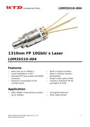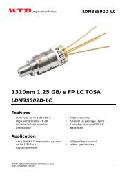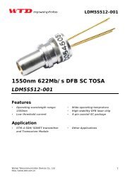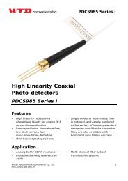
GPON OLT Optical Transceiver SFP Module RTXM167-522
GPON OLT Optical Transceiver SFP Module RTXM167-522
GPON OLT Optical Transceiver SFP Module RTXM167-522

Create successful ePaper yourself
Turn your PDF publications into a flip-book with our unique Google optimized e-Paper software.
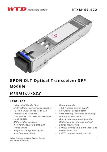
<strong>RTXM167</strong>-<strong>522</strong><strong>GPON</strong> <strong>OLT</strong> <strong>Optical</strong> <strong>Transceiver</strong> <strong>SFP</strong><strong>Module</strong><strong>RTXM167</strong>-<strong>522</strong>Features• Integrated Single fiberbi-directional optical subassembly• 1310nm Burst-mode APD/TIAreceiver and 1490nmContinuous DFB laser Transmitter(with WDM)• <strong>SFP</strong> metallic package• 0 to 70 o C operating ambienttemperature• Single SC receptacle opticalinterface compliantWuhan Telecommunication Devices Co., Ltd.http://www.wtd.com.cn• Hot-pluggable• +3.3V single power supply• Low power consumption• Fast settling time with immunityto long streams of CID• Guard time squelched function• Digitalized burst mode opticalpower monitoring• LVPECL compatible data input andoutput interface• LVTTL receiver reset control1
<strong>RTXM167</strong>-<strong>522</strong>• LVTTL receiverburst-power-detect indication• Class 1 Laser eye safety standard• Excellent EMI and EMCcharacteristics• ESD protection function• RoHs compliantApplication• <strong>Optical</strong> transceiver for Gigabit-capable Passive <strong>Optical</strong> Networks (<strong>GPON</strong>)Class B+ <strong>OLT</strong> sideStandard• ITU-T G.984.2 Class B+• Small Form-factor Pluggable (<strong>SFP</strong>) <strong>Transceiver</strong> Multisource Agreement July5, 2000DescriptionThe <strong>GPON</strong> <strong>OLT</strong> <strong>Transceiver</strong> is designed for Gigabit-capable Passive <strong>Optical</strong> Network(<strong>GPON</strong>)transmission. Themodule incorporates 1490nm DFB continuous-mode transmitter and 1310nm burst-mode APD receiver.The transmitter section uses a high efficiency 1490nm DFB laser and an integrated laser driver which isdesigned to be class-1 eye safety under any single fault. The laser driver includes APC and temperaturecompensation functions, which are used for keeping the launch optical power and extinction ratio constantover temperature and aging.The receiver section uses an integrated APD detector and burst mode preamplifier mounted together. Toprovide fast settling time with immunity to long streams of Consecutive Identical Digits(CID), the receiverrequires a reset signal provided by the media access controller(MAC). The receiver has fast SD function, therising time is about 5ns, when reset signal arrived, the SD signal will be turned to low, and the noise in theguard time will be squelched.The receiver includes digitalized burst mode optical power monitoring function, which converses any of areceived ONU optical power directly in digital, with a Trigger input from system. When rising edge of Triggerdetected, the DDM processor starts a burst optical power conversion, the digital result is available via DDMinterface after Burst <strong>Optical</strong> Power Conversion Time. Trigger pulse width should be more than Burst <strong>Optical</strong>Power Conversion Holding Time.An integrated WDM coupler can distinguish 1310nm input light from 1490nm output light.The metallic package guarantees excellent EMI and EMC characteristics, which totally comply withinternational relevant standards.Absolute Maximum RatingsParameter Symbol Unit Min MaxOperating Temperature RangeStorage Temperature RangeT cT so C 0 70o C -40 85Wuhan Telecommunication Devices Co., Ltd.http://www.wtd.com.cn2
<strong>RTXM167</strong>-<strong>522</strong>TimeBurst optical power conversion holding time HoldingTimens 400 Figure 2result can be read out sinceBurst optical power conversion time us 500 rising edge of the triggerpulseNote7: Measured with PRBS 2 23 -1 test pattern @1.244Gbps with Tx on, ER=10dB,BER
<strong>RTXM167</strong>-<strong>522</strong>Figure2 Trigger sequence definition in <strong>GPON</strong> systemMemory Map2 wire address 1010000X (A0) 2 wire address 1010001X(A2)095127Serial ID Defined bySPF MSA(96bytes)Vendor Specific(32bytes)Reserved in<strong>SFP</strong> MSA(128bytes)05595119127Alarm and WarningThresholds (56 bytes)Cal Constants(40 bytes)Real-Time DiagnosticInterface (24 bytes)Vendor Specific (8bytes)Vendor SpecificUser (136 bytes) WritableEEPROM(120bytes)255247255Vendor Specific(8bytes)Wuhan Telecommunication Devices Co., Ltd.http://www.wtd.com.cn6
<strong>RTXM167</strong>-<strong>522</strong>EEPROM Serial ID Memory ContentsAccessing Serial ID Memory uses the 2 wire address 1010000X (A0). Memory Contents of Serial ID are shownin Table below.Table 1 Serial ID Memory ContentsData SizeAddress (Bytes)Name of Field Contents(Hex) DescriptionBASE ID FIELDS0 1 Identifier 03 <strong>SFP</strong>1 1 Ext. Identifier 04<strong>SFP</strong> function is defined by serial IDonly2 1 Connector 01 Connector3-10 8 <strong>Transceiver</strong> 00 00 00 80 00 00 00 0011 1 Encoding 03 NRZ12 1 BR, Nominal 19 2488.32Mbps13 1 Reserved 0014 1 Length (9μm) km 1415 1 Length (9μm) 100m C816 1 Length (50μm) 10m 00<strong>Transceiver</strong> transmit distance 20km17 1 Length(62.5μm)10m 0018 1 Length (Copper) 00 Not compliant19 1 Reserved 0020-35 16 Vendor name57 54 44 20 20 20 20 2020 20 20 20 20 20 20 20“WTD”(ASCII)36 1 Reserved 0037-39 3 Vendor OUI 00 00 0040-55 16 Vendor PN52 54 58 4D 31 36 37 2D“<strong>RTXM167</strong>-<strong>522</strong>”35 32 32 20 20 20 20 20 <strong>Transceiver</strong> part number56-59 4 Vendor rev 20 20 20 2060-61 2 Wavelength 05 D2 1490nm TX wavelength62 1 Reserved 0063 1 CC_BASE Check Sum (Variable) Check code for Base ID FieldsEXTENDED ID FIELDS64-65 2 Options 00 1CTX_DISABLE, TX_FAULT and BurstPower Detect (SD) implemented.66 1 BR, max 0067 1 BR, min 0068-83 16 Vendor SN42 30 30 39 38 32 32 20 Serial Number of transceiver20 20 20 20 20 20 20 20 (ASCII). For example “B009822”.84-91 8 Date code 30 32 31 30 30 35 20 20Manufactory date code. For example“021005”.92 1 Diagnostic 60 DDM implemented, InternalWuhan Telecommunication Devices Co., Ltd.http://www.wtd.com.cn7
<strong>RTXM167</strong>-<strong>522</strong>Monitoring Typecalibration93 1 Enhanced Options 80 Alarm/warning flags implemented.94 1SFF-8472compliance02 Rev 9.4 of SFF-847295 1 CC_EXT Check Sum (Variable) Check sum for Extended ID Field.VENDOR SPECIFIC ID FIELDS96-127 32 Vendor Specific Read only Depends on customer information128-255 128 Reserved Read only Filled by zeroDiagnostic Monitor FunctionsDiagnostic Monitor Functions interface uses the 2 wire address 1010001X (A2). Memory contents ofDiagnostic Monitor Functions are shown in Table below.Table 2 Memory contents of Diagnostic Monitor FunctionData Field SizeAddress (bytes)NameContents and DescriptionAlarm and Warning Thresholds00-01 2 Temperature High Alarm Set to 80 o C02-03 2 Temperature Low Alarm Set to -13 o C04-05 2 Temperature High Warning Set to 75 o C06-07 2 Temperature Low Warning Set to -8 o C08-09 2 Vcc High Alarm Set to 3.6 V10-11 2 Vcc Low Alarm Set to 3.0 V12-13 2 Vcc High Warning Set to 3.5 V14-15 2 Vcc Low Warning Set to 3.1 V16-17 2 Bias High Alarm 90mA18-19 2 Bias Low Alarm 0mA20-21 2 Bias High Warning 70mA22-23 2 Bias Low Warning 0mA24-25 2 TX Power High Alarm +5.5dBm26-27 2 TX Power Low Alarm +0.5dBm28-29 2 TX Power High Warning +5dBm30-31 2 TX Power Low Warning +1dBm32-33 2 RX Power High Alarm -8dBm34-35 2 RX Power Low Alarm -30dBm36-37 2 RX Power High Warning -10dBm38-39 2 RX Power Low Warning -28dBm40-55 16 ReservedCalibration Constants56-59 4 RX Power Calibration Data4 Single precision floating-point numbers (various60-63 4 RX Power Calibration Data3values at each device)64-67 4 RX Power Calibration Data2 Single precision floating-point numbers (variousWuhan Telecommunication Devices Co., Ltd.http://www.wtd.com.cn8
<strong>RTXM167</strong>-<strong>522</strong>68-71 4 RX Power Calibration Data1 values at each device)72-75 4 RX Power Calibration Data076-77 2 Bias Calibration Data1 01 00 (fixed)78-79 2 Bias Calibration Data0 00 00 (fixed)80-81 2 TX Power Calibration Data1 01 00 (fixed)82-83 2 TX Power Calibration Data0 00 00 (fixed)84-85 2 Temperature Calibration Data1 01 00 (fixed)86-87 2 Temperature Calibration Data0 00 00 (fixed)88-89 2 Vcc Calibration Data1 01 00 (fixed)90-91 2 Vcc Calibration Data0 00 00 (fixed)92-94 3 Reserved 00 00 00 (fixed)95 1 Check Sum Checksum of bytes 0-94Real Time Diagnostic Monitor Interface96-97 2 Measured Temperature Yield to a 16-bit A/D value (see Table 2.1)98-99 2 Measured Vcc Yield a 16-bit A/D value (see Table 2.1)100-101 2 Measured Bias Yield a 16-bit A/D value (see Table 2.1)102-103 2 Measured TX Power Yield a 16-bit A/D value (see Table 2.1)104-105 2 Measured RX Power Yield a 16-bit A/D value (see Table 2.1)106-109 4 Reserved110 1 Logic Status See Table 2.2111 1 AD Conversion Updates See Table 2.2112-119 8 Alarm and Warning Flags See Table 2.3Vendor Specific120-127 8 Vendor Specific Don’t Access128-247 120 User writable EEPROM248-255 8 Vendor Specific Don’t AccessThe measured values located at bytes 96-105(in the 2 wire address 0xA2) are raw A/D values (16-bit integers)of transceiver temperature, supply voltage, laser bias current, laser optical output power and received power.All the measured values are “Externally Calibrated”, and then it is necessary to convert raw A/D values to realworld units by the manner as shown in Table 2.1Table 2.1 Real Time Diagnostic Monitor ValuesByte NameDescriptionTemperature96Internally measured transceiver temperature. Comply with External Calibration ofMSBSFF-8472.97 Temperature LSB98 Vcc MSB99 Vcc LSBInternally measured supply voltage. Comply with External Calibration of SFF-8472.100 Laser Bias MSBMeasured Laser bias current. Comply with External Calibration of SFF-8472.101 Laser Bias LSB102 Tx Power MSBMeasured Tx power. Comply with External Calibration of SFF-8472.103 Tx Power LSB104 Rx Power MSB Measured Rx power. Comply with External Calibration of SFF-8472.Wuhan Telecommunication Devices Co., Ltd.http://www.wtd.com.cn9
<strong>RTXM167</strong>-<strong>522</strong>105 Rx Power LSBThis transceiver implements two optional status bytes, “Logic States” at byte 110(0xA2)” and “A/D Updated”at byte 111(0xA2) as shown in Table 2.2. “A/D Updated” status bits allow the user to verify if an update fromthe analog-digital conversion has occurred of the measured values, temperature, Vcc, laser bias, Tx powerand Rx power. The user writes the byte to 0x00. Once a conversion is completed for a given value, its bit willchange to ‘1’.Table 2.2 Logic Status and AD Conversion UpdatesByte Bit Name Description110 7 Tx Disable State Optional digital State of the Tx Disable input pin.110 6 Soft Tx Disable Control Not supported (set to 0).110 5 Reserved Set to 0.110 4 Rx Rate Select State Not supported (set to 1).110 3 Soft Rate Select Control Not supported (set to 0).110 2 Tx Fault Optional digital state of the Tx Fault output pin.110 1 LOS Not supported.110 0 Power on Logic Bit will be 0 when the analog monitoring is active.111 7 Temp A/D Valid Indicates A/D value in Bytes 96/97 is valid.111 6 Vcc A/D Valid Indicates A/D value in Bytes 98/99 is valid.111 5 Laser Bias A/D Valid Indicates A/D value in Bytes 100/101 is valid.111 4 Tx Power A/D Valid Indicates A/D value in Bytes 102/103 is valid.111 3 Rx Power A/D Valid Indicates A/D value in Bytes 104/105 is valid.111 2 Reserved Set to 0.111 1 Reserved Set to 0.111 0 Reserved Set to 0.Each of the measured values has a corresponding high alarm, low alarm, high warning and low warningthreshold level at location 00-39(0xA2) written as the data format of a corresponding valued shown in Table2.3. Alarm and warning flags at bytes 112-119(0xA2) are defined as follows.(1) Alarm flags indicate conditions likely to result (or have resulted) in link failure and cause for immediateaction.(2) Warning flags indicate conditions outside the guaranteed operating specification of transceiver but notnecessarily causes of immediate link failures.Table 2.3 Alarm and Warning FlagsByte Bit(s) NameDescription112 7 Temperature High Alarm Set when temperature monitor value exceeds high alarm level.112 6 Temperature Low Alarm Set when temperature monitor value exceeds low alarm level.112 5 Vcc High Alarm Set when Vcc monitor value exceeds high alarm level.112 4 Vcc Low Alarm Set when Vcc monitor value exceeds Low alarm level.112 3 Laser Bias High Alarm Set when laser bias monitor value exceeds high alarm level.112 2 Laser Bias Low Alarm Set when laser bias monitor value exceeds low alarm level.112 1 Tx Power High Alarm Set when Tx power monitor value exceeds high alarm level112 0 Tx Power Low Alarm Set when Tx power monitor value exceeds low alarm level.113 7 Rx Power High Alarm Set when Rx power monitor value exceeds high alarm levelWuhan Telecommunication Devices Co., Ltd.http://www.wtd.com.cn10
<strong>RTXM167</strong>-<strong>522</strong>113 6 Rx Power Low Alarm Set when Rx power monitor value exceeds low alarm level113 5-0 Reserved All bits set to 0.114 7-0 Reserved All bits set to 0.115 7-0 Reserved All bits set to 0.116 7 Temperature High warning Set when temperature monitor value exceeds high warning level.116 6 Temperature Low warning Set when temperature monitor value exceeds low warning level.116 5 Vcc High warning Set when Vcc monitor value exceeds high warning level.116 4 Vcc Low warning Set when Vcc monitor value exceeds Low warning level.116 3 Laser Bias High warning Set when laser bias monitor value exceeds high warning level.116 2 Laser Bias Low warning Set when laser bias monitor value exceeds low warning level.116 1 Tx Power High warning Set when Tx power monitor value exceeds high warning level116 0 Tx Power Low warning Set when Tx power monitor value exceeds low warning level.117 7 Rx Power High warning Set when Rx power monitor value exceeds high warning level117 6 Rx Power Low warning Set when Rx power monitor value exceeds low warning level117 5-0 Reserved All bits set to 0.118 7-0 Reserved All bits set to 0.119 7-0 Reserved All bits set to 0.Pin DescriptionPin Name Function/Description Engagement order Notes1 VeeT Transmitter Ground 12 TX Fault Transmitter Fault Indication 3 13 TX Disable Transmitter Disable-<strong>Module</strong> disables on high or open 3 2Wuhan Telecommunication Devices Co., Ltd.http://www.wtd.com.cn11
<strong>RTXM167</strong>-<strong>522</strong>4 MOD-DEF2 <strong>Module</strong> Definition 2-Two wire serial ID interface 3 35 MOD-DEF1 <strong>Module</strong> Definition 1-Two wire serial ID interface 3 36 MOD-DEF0 <strong>Module</strong> Definition 0-Two wire serial ID interface 3 37 Reset Reset signal input 3 88 BPD Burst Power Detect (active HIGH) 3 49 Trigger Trigger input of burst signal packet received 3 910 VeeR Receiver Ground 111 VeeR Receiver Ground 112 RD- Inverted Received Data out 3 513 RD+ Received Data out 3 514 VeeR Receiver Ground 115 VccR Receiver Power supply, +3.3V±5% 2 616 VccT Transmitter Power supply, +3.3 V±5% 2 617 VeeT Transmitter Ground 118 TD+ Transmitter Data In 3 719 TD- Inverted Transmitter Data In 3 720 VeeT Transmitter Ground 1Note1: TX Fault is open collector/drain output which should be pulled up externally with a 4.7K – 10KΩresistor on the host board to supply
<strong>RTXM167</strong>-<strong>522</strong>Block diagramTypical application circuitWuhan Telecommunication Devices Co., Ltd.http://www.wtd.com.cn13
<strong>RTXM167</strong>-<strong>522</strong>Package outlineUnits in mmRegulatory ComplianceFeature Test Method PerformanceElectrostatic Discharge (ESD)to the Electrical PinsElectrostatic Discharge (ESD)ImmunityElectromagnetic Interference(EMI)ImmunityEye SafetyMIL-STD-883EMethod 3015.7IEC61000-4-2CISPR22 ITE Class BEN55022 Class BIEC61000-4-3 Class 2EN55024FDA 21 CFR 1040.10and 1040.11ULTUV EN 60825-1Class 1 (>1.5kV) – Human Body ModelClass 2(>4.0kV)Compliant with standardsTypically show no measurable effect from a 3V/mfield swept from 80 to 1000MHz applied to thetransceiver without a chassis enclosure.Compliant with Class 1 laser productWuhan Telecommunication Devices Co., Ltd.http://www.wtd.com.cn14
<strong>RTXM167</strong>-<strong>522</strong>Ordering informationPart No.TXPackageData RateLaserStandardSpecification<strong>Optical</strong>RXPowerDetectorSensitivity TempData RateApplicationCode<strong>RTXM167</strong>-<strong>522</strong> <strong>SFP</strong> 2.488Gb/s 1490nmDFB1.5~5dBm APD 1.244Gb/s