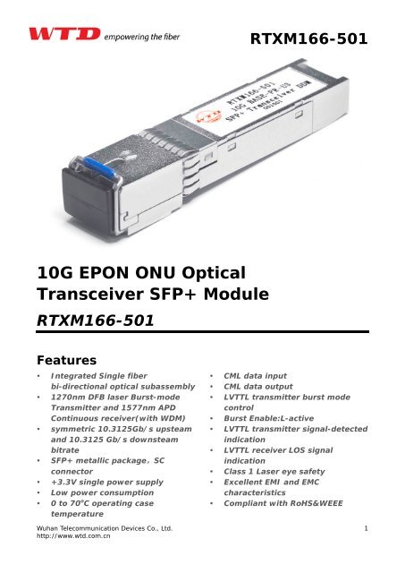
RTXM166-501
RTXM166-501
RTXM166-501

You also want an ePaper? Increase the reach of your titles
YUMPU automatically turns print PDFs into web optimized ePapers that Google loves.
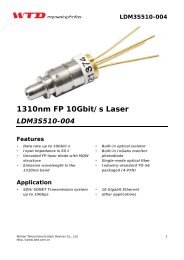
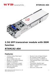
10G EPON ONU Optical<br />
Transceiver SFP+ Module<br />
<strong>RTXM166</strong>-<strong>501</strong><br />
Features<br />
� Integrated Single fiber<br />
bi-directional optical subassembly<br />
� 1270nm DFB laser Burst-mode<br />
Transmitter and 1577nm APD<br />
Continuous receiver(with WDM)<br />
� symmetric 10.3125Gb/s upsteam<br />
and 10.3125 Gb/s downsteam<br />
bitrate<br />
� SFP+ metallic package,SC<br />
connector<br />
� +3.3V single power supply<br />
� Low power consumption<br />
� 0 to 70 o C operating case<br />
temperature<br />
Wuhan Telecommunication Devices Co., Ltd.<br />
http://www.wtd.com.cn<br />
<strong>RTXM166</strong>-<strong>501</strong><br />
� CML data input<br />
� CML data output<br />
� LVTTL transmitter burst mode<br />
control<br />
� Burst Enable:L-active<br />
� LVTTL transmitter signal-detected<br />
indication<br />
� LVTTL receiver LOS signal<br />
indication<br />
� Class 1 Laser eye safety<br />
� Excellent EMI and EMC<br />
characteristics<br />
� Compliant with RoHS&WEEE<br />
1
Applications<br />
Wuhan Telecommunication Devices Co., Ltd.<br />
http://www.wtd.com.cn<br />
<strong>RTXM166</strong>-<strong>501</strong><br />
� 20Km Symmetric 10 Gigabit Ethernet Access over PON Networks<br />
Standard<br />
� IEEE802.3av, 2009<br />
10GBASE-PR-U3<br />
� SFF-8432 Specification for<br />
Description<br />
Improved Pluggable Formfactor,<br />
Revision 4.3: 2007.5<br />
� Compliant with SFF-8472 v9.5<br />
The EPON ONU Transceiver is designed for 10G EPON transmission. The module incorporates 10.3125Gb/s<br />
1270nm burst-mode transmitter and 10.3125Gb/s 1577nm continuous-mode receiver. The transmitter<br />
section uses a 1270nm DFB laser and an integrated BM laser driver which designed to perform very small<br />
burst enable/disable delay time. The laser driver also includes digital APC and temperature compensation<br />
circuit, which are used for keeping the launch optical power and extinction ratio constant over temperature<br />
and aging.<br />
The receiver section uses an integrated 1577nm APD photodiode and preamplifier mounted together. It has<br />
the function that indicates receiver los status (active high).<br />
An integrated WDM coupler can separate 1577nm input light and 1270nm output light.<br />
The metallic package guarantees excellent EMI and EMC characteristics, which totally comply with<br />
international relevant standards.<br />
Absolute Maximum Ratings<br />
Parameter Symbol Unit Min Max<br />
Operating ambient Temperature Range T op<br />
Storage Temperature Range T s<br />
o C 0 70<br />
o C -40 85<br />
Relative Humidity RH % 5 95<br />
Power Supply Voltage V cc V 0 4.6<br />
Pin Input Voltage V GND Vcc<br />
Reciever Damage Threshold dBm -9 -<br />
Recommended operating conditions<br />
Parameter Symbol Unit Min Typ Max<br />
Operating Voltage V cc V 3.13 3.3 3.47<br />
Operating case Temperature Range T c<br />
o C 0 – 70<br />
2
Specifications (0°C
Within 15% of optical<br />
steady state<br />
Optical signal output of ONU module<br />
Tx_BEN of ONU module<br />
Electrical signal output of OLT module<br />
Ton<br />
Wuhan Telecommunication Devices Co., Ltd.<br />
http://www.wtd.com.cn<br />
Settling<br />
time<br />
Invalid<br />
date<br />
//<br />
//<br />
//<br />
Valid date<br />
Figure 1. Burst_mode Receiver Dynamic range in 10G EPON system<br />
Figure 2. Mask of diagram<br />
<strong>RTXM166</strong>-<strong>501</strong><br />
Toff<br />
Average launch<br />
power of off<br />
transmitter<br />
4
Digital Diagnostic Memory Map<br />
0<br />
95<br />
127<br />
255<br />
Wuhan Telecommunication Devices Co., Ltd.<br />
http://www.wtd.com.cn<br />
<strong>RTXM166</strong>-<strong>501</strong><br />
2 wire address 1010000X (A0) 2 wire address 1010001X(A2)<br />
Serial ID Defined by<br />
SPF MSA(96bytes)<br />
Vendor Specific<br />
(32bytes)<br />
Reserved in<br />
SFP MSA<br />
(128bytes)<br />
0<br />
55<br />
95<br />
119<br />
127<br />
247<br />
255<br />
Alarm and Warning<br />
Thresholds (56 bytes)<br />
Cal Constants<br />
(40 bytes)<br />
Real-Time Diagnostic<br />
Interface (24 bytes)<br />
EEPROM Serial ID Memory Contents<br />
Vendor Specific (8bytes)<br />
Vendor Specific<br />
User (136 bytes) Writable<br />
EEPROM(120bytes)<br />
Vendor Specific(8bytes)<br />
Accessing Serial ID Memory uses the 2 wire address 1010000X (A0). Memory Contents of Serial ID are shown<br />
in the Table 1.<br />
Table 1 Serial ID Memory Contents<br />
Data Size<br />
Address (Bytes)<br />
Name of Field Contents(Hex) Description<br />
BASE ID FIELDS<br />
0 1 Identifier 03 SFP<br />
1 1 Extended. Identifier 04<br />
GBIC/SFP function is defined by serial ID<br />
only<br />
2 1 Connector 01 SC<br />
3-10 8 Transceiver 03 Transceiver Codes<br />
11 1 Encoding 03 NRZ<br />
12 1 BR, Nominal 67 10.3125Gbit/sec<br />
13 1 Reserved 00<br />
14 1 Length (9μm) km 14<br />
15 1 Length (9μm) 100m C8<br />
16 1 Length (50μm) 10m 00<br />
17 1 Length(62.5μm)10m 00<br />
Transceiver transmit distance<br />
5
Wuhan Telecommunication Devices Co., Ltd.<br />
http://www.wtd.com.cn<br />
<strong>RTXM166</strong>-<strong>501</strong><br />
18 1 Length (Copper) 00 Not compliant<br />
19 1 Reserved 00<br />
20-35 16 Vendor name<br />
57 54 44 FF FF FF FF FF<br />
20 20 20 20 20 20 20 20<br />
36 1 Reserved 00<br />
37-39 3 Vendor OUI 00 1C AD<br />
40-55 16 Vendor PN<br />
52 54 58 4D 31 36 36 2D<br />
35 30 31 20 20 20 20 20<br />
“WTD”(ASCII)<br />
“<strong>RTXM166</strong>-<strong>501</strong>”<br />
56-59 4 Vendor rev 31 2E 30 20 1.0<br />
60-61 2 Wavelength 04 F6 1270<br />
62 1 Reserved 00<br />
63 1 CC_BASE Check Sum (Variable) Check code for Base ID Fields<br />
EXTENDED ID FIELDS<br />
64-65 2 Options 00 0A<br />
66 1 BR,max 00<br />
67 1 BR,min 00<br />
68-83 16 Vendor SN<br />
42 30 30 39 38 32 32 20<br />
20 20 20 20 20 20 20 20<br />
84-91 8 Date code 30 32 31 30 30 35 20 20<br />
92 1<br />
Diagnostic<br />
Monitoring Type<br />
93 1 Enhanced Options E0<br />
94 1<br />
SFF_8472<br />
Compliance<br />
68<br />
02<br />
TX_FAULT and Loss of Signal are<br />
implemented.<br />
Serial Number of transceiver (ASCII).<br />
For example “B009822”.<br />
Manufactory date code. For example<br />
“021005”.<br />
Digital diagnostic monitoring<br />
implemented, “internally calibrated” is<br />
implemented, RX measurement type is<br />
“Average Power”.<br />
Optional Alarm/Warning flags<br />
implemented for all monitored<br />
quantities<br />
Optional Soft TX_DISABLE control and<br />
monitoring implemented,<br />
Optional Soft TX_FAULT monitoring<br />
implemented,<br />
Includes functionality described in<br />
Rev9.5 SFF-8472.<br />
95 1 CC_EXT Check Sum (Variable) Check sum for Extended ID Field.<br />
VENDOR SPECIFIC ID FIELDS<br />
96-127 32 Vendor Specific Read only Depends on customer information<br />
128-255 128 Reserved Read only Filled by zero<br />
Data<br />
Address<br />
Field Size<br />
(bytes)<br />
Table 2 Memory contents of Diagnostic Monitor Function<br />
Name Contents and Description<br />
Alarm and Warning Thresholds<br />
6
Wuhan Telecommunication Devices Co., Ltd.<br />
http://www.wtd.com.cn<br />
<strong>RTXM166</strong>-<strong>501</strong><br />
00-01 2 Temperature High Alarm Set to 80 O C<br />
02-03 2 Temperature Low Alarm Set to -5 O C<br />
04-05 2 Temperature High Warning Set to 70 O C<br />
06-07 2 Temperature Low Warning Set to 0 O C<br />
08-09 2 Vcc High Alarm Set to 3.6 V<br />
10-11 2 Vcc Low Alarm Set to 3.0 V<br />
12-13 2 Vcc High Warning Set to 3.5 V<br />
14-15 2 Vcc Low Warning Set to 3.1 V<br />
16-17 2 Bias High Alarm 75mA<br />
18-19 2 Bias Low Alarm 2 mA<br />
20-21 2 Bias High Warning 60 mA<br />
22-23 2 Bias Low Warning 5 mA<br />
24-25 2 TX Power High Alarm 11.0dbm<br />
26-27 2 TX Power Low Alarm 2.0dbm<br />
28-29 2 TX Power High Warning 9.0dbm<br />
30-31 2 TX Power Low Warning 4.0dbm<br />
32-33 2 RX Power High Alarm -9.0dbm<br />
34-35 2 RX Power Low Alarm -29.5dbm<br />
36-37 2 RX Power High Warning -10.0dbm<br />
38-39 2 RX Power Low Warning -28.5dbm<br />
40-55 16 Reserved<br />
Calibration Constants<br />
56-59 4 RX Power Calibration Data4 00 00 00 00 (fixed)<br />
60-63 4 RX Power Calibration Data3 00 00 00 00 (fixed)<br />
64-67 4 RX Power Calibration Data2 00 00 00 00 (fixed)<br />
68-71 4 RX Power Calibration Data1 3F 80 00 00 (fixed)<br />
72-75 4 RX Power Calibration Data0 00 00 00 00 (fixed)<br />
76-77 2 Bias Calibration Data1 01 00 (fixed)<br />
78-79 2 Bias Calibration Data0 00 00 (fixed)<br />
80-81 2 TX Power Calibration Data1 01 00 (fixed)<br />
82-83 2 TX Power Calibration Data0 00 00 (fixed)<br />
84-85 2 Temperature Calibration Data1 01 00 (fixed)<br />
86-87 2 Temperature Calibration Data0 00 00 (fixed)<br />
88-89 2 Vcc Calibration Data1 01 00 (fixed)<br />
90-91 2 Vcc Calibration Data0 00 00 (fixed)<br />
92-94 3 Reserved 00 00 00 (fixed)<br />
95 1 Check Sum Checksum of bytes 0-94<br />
Real Time Diagnostic Monitor Interface 1<br />
96-97 2 Measured Temperature Internally measured module temperature<br />
7
Wuhan Telecommunication Devices Co., Ltd.<br />
http://www.wtd.com.cn<br />
<strong>RTXM166</strong>-<strong>501</strong><br />
98-99 2 Measured Vcc Internally measured supply voltage in module<br />
100-101 2 Measured Bias Internally measured Tx Bias current<br />
102-103 2 Measured TX Power Internally measured Tx Optical Power<br />
104-105 2 Measured RX Powe r Measured Rx input power<br />
106-109 4 Reserved<br />
110 1 Logic Status See Table 2.1<br />
111 1 AD Conversion Updates See Table 2.1<br />
112-119 8 Alarm and Warning Flags See Table 2.2<br />
Vendor Specific<br />
120-127 8 Vendor Specific Don’t Access<br />
128-247 120 User writable EEPROM<br />
248-255 8 Vendor Specific Don’t Access<br />
Note1: Temperature (Signed twos complement value)<br />
S 2 6<br />
A2h Byte 96 (Temperature MSB) A2h Byte 97 (Temperature LSB)<br />
2 5<br />
2 4<br />
2 3<br />
2 2<br />
2 1<br />
Supply Voltage, Tx Bias Current, Tx Optical Power, Rx Received Power (Unsigned values)<br />
2 0<br />
A2h Byte 98 (Vcc MSB) A2h Byte 99 (Vcc LSB)<br />
A2h Byte 98 (Vcc MSB) A2h Byte 99 (Vcc LSB)<br />
A2h Byte 102 (TX Power MSB) A2h Byte 103 (TX Power LSB)<br />
A2h Byte 104 (RX Power MSB) A2h Byte 105 (RX Power LSB)<br />
2 15 2 14 2 13 2 12 2 11 2 10 2 9 2 8 2 7 2 6 2 5 2 4 2 3 2 2 2 1 2 0<br />
All the measured values are “Internally Calibrated”,Each measurement could be obtained by multiplying<br />
digital value by corresponding LSB value:<br />
Temperature = Temp (Digital Value) × (1/256); when Temperature
Wuhan Telecommunication Devices Co., Ltd.<br />
http://www.wtd.com.cn<br />
<strong>RTXM166</strong>-<strong>501</strong><br />
Each of the measured values has a corresponding high alarm, low alarm, high warning and low warning<br />
threshold level at location 00-39(x0A2) written as the data format of a corresponding valued shown in Table<br />
2.2.Alarm and warning flags at bytes 112-119(0xA2) are defined as follows.<br />
(1) Alarm flags indicate conditions likely to result (or have resulted) in link failure and cause for immediate<br />
action.<br />
(2) Warning flags indicate conditions outside the guaranteed operating specification of transceiver but not<br />
necessarily causes of immediate link failures.<br />
Table 2.2 Alarm and Warning Flags<br />
Byte Bit(s) Name Description<br />
112 7 Temperature High Alarm Set when temperature monitor value exceeds high alarm level.<br />
112 6 Temperature Low Alarm Set when temperature monitor value exceeds low alarm level.<br />
112 5 Vcc High Alarm Set when Vcc monitor value exceeds high alarm level.<br />
112 4 Vcc Low Alarm Set when Vcc monitor value exceeds Low alarm level.<br />
112 3 Laser Bias High Alarm Set when laser bias monitor value exceeds high alarm level.<br />
112 2 Laser Bias Low Alarm Set when laser bias monitor value exceeds low alarm level.<br />
112 1 Tx Power High Alarm Set when Tx power monitor value exceeds high alarm level<br />
112 0 Tx Power Low Alarm Set when Tx power monitor value exceeds low alarm level.<br />
113 7 Rx Power High Alarm Set when Rx power monitor value exceeds high alarm level<br />
113 6 Rx Power Low Alarm Set when Rx power monitor value exceeds low alarm level<br />
113 5-0 Reserved All bits set to 0.<br />
114 7-0 Reserved All bits set to 0.<br />
115 7-0 Reserved All bits set to 0.<br />
116 7 Temperature High warning<br />
116 6 Temperature Low warning<br />
Set when temperature monitor value exceeds high warning<br />
level.<br />
Set when temperature monitor value exceeds low warning<br />
level.<br />
116 5 Vcc High warning Set when Vcc monitor value exceeds high warning level.<br />
116 4 Vcc Low warning Set when Vcc monitor value exceeds Low warning level.<br />
116 3 Laser Bias High warning Set when laser bias monitor value exceeds high warning level.<br />
116 2 Laser Bias Low warning Set when laser bias monitor value exceeds low warning level.<br />
116 1 Tx Power High warning Set when Tx power monitor value exceeds high warning level<br />
116 0 Tx Power Low warning Set when Tx power monitor value exceeds low warning level.<br />
117 7 Rx Power High warning Set when Rx power monitor value exceeds high warning level<br />
117 6 Rx Power Low warning Set when Rx power monitor value exceeds low warning level<br />
117 5-0 Reserved All bits set to 0.<br />
118 7-0 Reserved All bits set to 0.<br />
119 7-0 Reserved All bits set to 0.<br />
9
Pin Description<br />
Wuhan Telecommunication Devices Co., Ltd.<br />
http://www.wtd.com.cn<br />
<strong>RTXM166</strong>-<strong>501</strong><br />
Pin Name Description Pin Name Description<br />
1 GND_T Transmitter ground 20 GND_T Transmitter ground<br />
2 TX_FAULT<br />
3 TX_BRST<br />
LVTTL Signal detect output,<br />
internally pull up<br />
LVTTL Transmitter burst mode<br />
control, “L”: Tx ON<br />
19 TD-(10G)<br />
18 TD+(10G)<br />
CML Data input-<br />
(AC coupled internally)<br />
CML Data input+<br />
(AC coupled internally)<br />
4 SDA I 2 C Serial Data (LVTTL) 17 GND_T Transmitter ground<br />
5 SCL I 2 C Serial Clock(LVTTL) 16 VCC_T Transmitter power supply<br />
6 MOS_ABS Internally connected GND 15 VCC_R Receiver power supply<br />
7 TX-SD<br />
8 RX_LOS<br />
LVTTL Signal detect output,<br />
internally pull up<br />
LVTTL Signal detect output,<br />
internally pull up<br />
14 GND_R Receiver ground<br />
13 RD+(10G)<br />
9 NC 12 RD-(10G)<br />
CML data output+<br />
(AC coupled internally)<br />
CML data output-<br />
(AC coupled internally)<br />
10 GND_R Receiver ground 11 GND_R Receiver ground<br />
Block Diagram<br />
WDM<br />
1577nm<br />
1270nm<br />
APD Bias<br />
APD +<br />
TIA<br />
LD/PD<br />
Digital Diagnostic<br />
Monitoring<br />
EEPROM<br />
LA<br />
Burst LD Driver<br />
MCU<br />
Figure3 Functional block diagram<br />
CML RD+/-<br />
LVTTL LOS<br />
CML TD+/-<br />
LVTTL BEN<br />
LVTTL FAULT<br />
LVTTL SD<br />
SDA<br />
SCL<br />
10
Typical Application Circuit<br />
<strong>RTXM166</strong>-401<br />
Laser<br />
Driver<br />
TIA<br />
+Limiting<br />
Amplifier<br />
I2C Slave<br />
Package Outline<br />
TD+(18)<br />
TD-(19)<br />
Wuhan Telecommunication Devices Co., Ltd.<br />
http://www.wtd.com.cn<br />
Tx Vcc(16)<br />
1.2uH<br />
+3.3V<br />
0.1uF 10uF 10uF<br />
Tx GND(1 17 20)<br />
Tx FAULT(2)<br />
Tx SD(7)<br />
Tx EN(3)<br />
RD+(13)<br />
RD-(12)<br />
LOS(8)<br />
Rx Vcc(15)<br />
Zo=50Ω<br />
Zo=50Ω<br />
1.2uH<br />
0.1uF 10uF 10uF<br />
Rx GND(10 11 14)<br />
SDA(4)<br />
SCL(5)<br />
Zo=50Ω<br />
Zo=50Ω<br />
+3.3V<br />
+3.3V<br />
2*(4.7-10K)<br />
Figure4 Typical application circuit<br />
Figure5 Package outline<br />
<strong>RTXM166</strong>-<strong>501</strong><br />
Serial data output+<br />
Serial data output-<br />
Fault Indicator<br />
Sd Indicator<br />
Tx Control<br />
Serial data input+<br />
Serial data input-<br />
LOS Indicator<br />
SDA<br />
SCL<br />
10G EPON<br />
ONU<br />
SYSTEM<br />
11
Regulatory Compliance<br />
Wuhan Telecommunication Devices Co., Ltd.<br />
http://www.wtd.com.cn<br />
<strong>RTXM166</strong>-<strong>501</strong><br />
Feature Test Method Performance<br />
Electrostatic Discharge<br />
(ESD) to the Electrical Pins<br />
Electrostatic Discharge<br />
(ESD) Immunity<br />
Electromagnetic<br />
Interference (EMI)<br />
Immunity<br />
Eye Safety<br />
MIL-STD-883E<br />
Method 3015.7<br />
Class 1 (>1.5kV) – Human Body Model<br />
IEC61000-4-2 Class 2(>4.0kV)<br />
CISPR22 ITE Class B<br />
EN55022 Class B<br />
IEC61000-4-3 Class 2<br />
EN55024<br />
FDA 21 CFR 1040.10<br />
and 1040.11<br />
UL<br />
TUV EN 60825-1<br />
Ordering Information<br />
Part No<br />
<strong>RTXM166</strong>-<strong>501</strong> SFP+<br />
Note1: SC connector.<br />
Compliant with standards<br />
Typically show no measurable effect from a 3V/m<br />
field swept from 80 to 1000MHz applied to the<br />
transceiver without a chassis enclosure.<br />
Compliant with Class 1 laser product<br />
Specification Application<br />
Package Datarate Laser Optical Power Detector Sensitivity Temp BM control logic<br />
10.3125Gb/s US<br />
10.3125Gb/s DS<br />
Code<br />
1270nm DFB +4~ +9dBm APD -28.5dBm 0~70°C L Enable 10G/10G EPON<br />
WTD reserves the right to make changes to the product(s) or information contained herein without notice. No<br />
liability is assumed as a result of their use or application. No rights under any patent accompany the sale of<br />
any such product(s) or information.<br />
Edition 2010-12-30<br />
Published by Wuhan Telecommunication Devices Co.,Ltd.<br />
Copyright © WTD<br />
All Rights Reserved.<br />
12