RTXM168-418
RTXM168-418
RTXM168-418
- No tags were found...
Create successful ePaper yourself
Turn your PDF publications into a flip-book with our unique Google optimized e-Paper software.
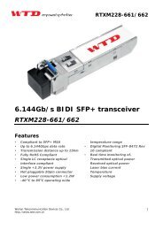
<strong>RTXM168</strong>-<strong>418</strong>EPON OLT Optical Transceiver SFPModule<strong>RTXM168</strong>-<strong>418</strong>Features• Integrated Single fiberbi-directional optical subassembly• 1310nm Burst-mode APD/TIAreceiver and 1490nmContinuous DFB laser Transmitter(with WDM)• SFP metallic package• 0 to 70 o C operating ambienttemperature• Single SC receptacle opticalinterface compliant• Hot-pluggable• +3.3V single power supply• Low power consumption• Resetless burst-mode receiver• Wide dynamic range over 20dB• Settling time less than 400ns• Digitalized burst mode opticalpower monitoring• LVPECL compatible AC coupledWuhan Telecommunication Devices Co., Ltd.http://www.wtd.com.cn1
<strong>RTXM168</strong>-<strong>418</strong>data input interface• LVPECL compatible DC coupleddata output interface• LVTTL transmitter laser shutdown• LVTTL receiverburst-power-detect indication• Class 1 Laser eye safety standard• Excellent EMI and EMCcharacteristics• ESD protection functionApplications• Optical transceiver for PX20+ of Gigabit Ethernet Passive Optical Networks(EPON) OLT sideStandards• IEEE802.3ah 1000BASE-PX20+DescriptionThe EPON OLT Transceiver module is designed for PX20+ of Gigabit Ethernet Passive Optical Network(EPON)20km transmission. The module incorporates 1490nm continuous-mode transmitter and 1310nm burst-modereceiver.The transmitter section uses a 1490nm DFB laser and an integrated laser driver which is designed to beclass-1 eye safe under any single fault. The laser driver includes APC and temperature compensationfunctions, which are used for keeping the launch optical power and extinction ratio constant over temperatureand aging.The receiver section uses an integrated APD and BM-preamplifier mounted together. The burst-mode receiveris resetless and wide dynamic range over 20dB can be obtained under whole operating conditions. Themodule has the function that indicates receiver burst-power-detect signal (active LOW).The receiver includes digitalized burst mode optical power monitoring function, which converses any of areceived ONU optical power directly in digital, with a Trigger input from system. When rising edge of Triggerdetected, the DDM processor starts a burst optical power conversion, the digital result is available via DDMinterface after Burst Optical Power Conversion Time. Trigger pulse width should be more than Burst OpticalPower Conversion Holding Time.An integrated WDM coupler can distinguish 1310nm input light from 1490nm output light.The metallic package guarantees excellent EMI and EMC characteristics.Absolute Maximum RatingsParameter Symbol Unit Min MaxOperating Temperature RangeStorage Temperature RangeT cT so C 0 70o C -40 85Relative Humidity RH % 5 95Power Supply Voltage V cc V 0 4.6Wuhan Telecommunication Devices Co., Ltd.http://www.wtd.com.cn2
<strong>RTXM168</strong>-<strong>418</strong>Optical receive CharacteristicsData Rate Mbps – 1250 –Receiver Sensitivity S dBm – – -30 Note6Overload Input Optical Power P in dBm -6 – – Note6Center Wavelength Range λ c nm 1260 1310 1360Reciever Settling Time T settling ns – – 400 Note8Reciever Dynamic range dB 20 – – Note9Receiver reflectance dB – – -12 λ=1.31µmBPD(LVTTL)Optical Dessert-45 – – Note11dBmOptical Assert – – -31BPD Hysteresis dB 0.5 – 6 Note11Measurement Accuracy of received burst opticalpower, range from -10dBm to -30dBmdB -1 +1Burst optical power conversion settling timeBOPCSTimens 250 Figure 1Burst optical power conversion holding timeHoldingTimens 400 Figure 1Burst optical power conversion time us 500Burst optical power conversion interval time ms 1.0result can be read outsince trigger is HighMeans 1000 conversions/smax.Note6: Measured with PRBS 2 7 -1 test pattern @1.25Gbps with Tx on,ER=10dB,BER
<strong>RTXM168</strong>-<strong>418</strong>Figure1 Time parameter definition in EPON system20dFigure2 Burst_mode Receiver Dynamic range in EPON systemWuhan Telecommunication Devices Co., Ltd.http://www.wtd.com.cn5
<strong>RTXM168</strong>-<strong>418</strong>Memory Map2 wire address 1010000X (A0) 2 wire address 1010001X (A2)095127Serial ID Defined bySFP MSA (96bytes)Vendor Spectific(32bytes)05595119127Alarm and WarningThresholds (56bytes)Cal Constants(40bytes)Real-Time DiagnosticInterface (24bytes)Vendor Specific(8bytes)Reserved inSFP MSA(128bytes)User WritableEEPROM(102bytes)255247255Vendor Specific(8bytes)EEPROM Serial ID Memory ContentsAccessing Serial ID Memory uses the 2 wire address 1010000X (A0). Memory Contents of Serial ID are shownin Table below.Table 1 Se rial ID Memory ContentsData SizeAddress (Bytes)Name of Field Contents(Hex) DescriptionBASE ID FIELDS0 1 Identifier 03 SFP1 1 Ext. Identifier 04 SFP function is defined by serial ID only2 1 Connector 01 Connector3-10 8 Transceiver 00 00 00 80 00 00 00 00 1000BASE-PX11 1 Encoding 01 8B10B12 1 BR, Nominal 0D 1250Mbps13 1 Reserved 0014 1 Length (9μm) km 1415 1 Length (9μm) 100m C816 1 Length (50μm) 10m 00Transceiver transmit distance 20km17 1 Length(62.5μm)10m 0018 1 Length (Copper) 00 Not compliantWuhan Telecommunication Devices Co., Ltd.http://www.wtd.com.cn6
<strong>RTXM168</strong>-<strong>418</strong>19 1 Reserved 0020-35 16 Vendor name57 54 44 20 20 20 20 2020 20 20 20 20 20 20 20“WTD”(ASCII)36 1 Reserved 0037-39 3 Vendor OUI 00 00 0040-55 16 Vendor PN52 54 58 4D 31 36 38 2D“<strong>RTXM168</strong>-<strong>418</strong>”34 31 38 20 20 20 20 20 Transceiver part number56-59 4 Vendor rev 20 20 20 2060-61 2 Wavelength 05 D2 1490nm downstream TX62 1 Reserved 0063 1 CC_BASE Check Sum (Variable) Check code for Base ID FieldsEXTENDED ID FIELDS64-65 2 Options 00 1ATX_DISABLE, TX_FAULT and BurstPower Detect implemented.66 1 BR,max 0067 1 BR,min 0068-83 16 Vendor SN42 30 30 39 38 32 32 20 Serial Number of transceiver (ASCII).20 20 20 20 20 20 20 20 For example “B009822”.84-91 8 Date codeManufactory date code. For example30 32 31 30 30 35 20 20“021005”.92 1DiagnosticMonitoring Type60 DDM implemented, internal calibration93 1 Enhanced Options 80 Alarm/warning flags implemented.94 1 SFF-8472 compliance 02 Rev 9.5 of SFF-847295 1 CC_EXT Check Sum (Variable) Check sum for Extended ID Field.VENDOR SPECIFIC ID FIELDS96-127 32 Vendor Specific Read only Depends on customer information128-255 128 Reserved Read only Filled by zeroDiagnostic Monitor FunctionsDiagnostic Monitor Functions interface uses the 2 wire address 1010001X (A2). Memory contents ofDiagnostic Monitor Functions are shown in Table belowTable 2 Memory contents of Diagnostic Monitor FunctionData Field SizeAddress (bytes)NameContents and DescriptionAlarm and Warning Thresholds00-01 2 Temperature High Alarm Set to 85 o C02-03 2 Temperature Low Alarm Set to -5 o C04-05 2 Temperature High Warning Set to 75 o C06-07 2 Temperature Low Warning Set to 0 o CWuhan Telecommunication Devices Co., Ltd.http://www.wtd.com.cn7
<strong>RTXM168</strong>-<strong>418</strong>08-09 2 Vcc High Alarm Set to 3.6 V10-11 2 Vcc Low Alarm Set to 3.0 V12-13 2 Vcc High Warning Set to 3.5 V14-15 2 Vcc Low Warning Set to 3.1 V16-17 2 Bias High Alarm 50mA18-19 2 Bias Low Alarm 3.75mA20-21 2 Bias High Warning 40mA22-23 2 Bias Low Warning 7.5mA24-25 2 TX Power High Alarm +7dBm26-27 2 TX Power Low Alarm +2.5dBm28-29 2 TX Power High Warning +6dBm30-31 2 TX Power Low Warning +3.5dBm32-33 2 RX Power High Alarm -6dBm34-35 2 RX Power Low Alarm -33dBm36-37 2 RX Power High Warning -9dBm38-39 2 RX Power Low Warning -30dBm40-55 16 ReservedCalibration Constants56-59 4 RX Power Calibration Data4 Single precision floating-point numbers (various60-63 4 RX Power Calibration Data3 values at each device)64-67 4 RX Power Calibration Data2Single precision floating-point numbers (various68-71 4 RX Power Calibration Data1values at each device)72-75 4 RX Power Calibration Data076-77 2 Bias Calibration Data1 01 00 (fixed)78-79 2 Bias Calibration Data0 00 00 (fixed)80-81 2 TX Power Calibration Data1 01 00 (fixed)82-83 2 TX Power Calibration Data0 00 00 (fixed)84-85 2 Temperature Calibration Data1 01 00 (fixed)86-87 2 Temperature Calibration Data0 00 00 (fixed)88-89 2 Vcc Calibration Data1 01 00 (fixed)90-91 2 Vcc Calibration Data0 00 00 (fixed)92-94 3 Reserved 00 00 00 (fixed)95 1 Check Sum Checksum of bytes 0-94Real Time Diagnostic Monitor Interface96-97 2 Measured Temperature Yield to a 16-bit A/D value (see Table 2.1)98-99 2 Measured Vcc Yield a 16-bit A/D value (see Table 2.1)100-101 2 Measured Bias Yield a 16-bit A/D value (see Table 2.1)102-103 2 Measured TX Power Yield a 16-bit A/D value (see Table 2.1)104-105 2 Measured RX Power Yield a 16-bit A/D value (see Table 2.1)106-109 4 Reserved110 1 Logic Status See Table 2.2Wuhan Telecommunication Devices Co., Ltd.http://www.wtd.com.cn8
<strong>RTXM168</strong>-<strong>418</strong>111 1 AD Conversion Updates See Table 2.2112-119 8 Alarm and Warning Flags See Table 2.3Vendor Specific120-127 8 Vendor Specific Don’t Access128-247 120 User writable EEPROM248-255 8 Vendor Specific Don’t AccessThe measured values located at bytes 96-105(in the 2 wire address 0xA2) are raw A/D values (16-bit integers)of transceiver temperature, supply voltage, laser bias current, laser optical output power and received power.All the measured values are “Internally Calibrated”, and then it is necessary to convert raw A/D values to realworld units by the manner as shown in Table 2.1Table 2.1 Real Time Diagnostic Monitor ValuesByte Name Description96 Temperature MSB Internally measured transceiver temperature. Comply with Internal97 Temperature LSB Calibration of SFF-8472.98 Vcc MSB Internally measured supply voltage. Comply with Internal Calibration of99 Vcc LSBSFF-8472.100 Laser Bias MSB101 Laser Bias LSBMeasured Laser bias current. Comply w ith Internal Calibration of SFF-8472.102 Tx Power MSB103 Tx Power LSBMeasured Tx power. Comply with Internal Calibration of SFF-8472.104 Rx Power MSB105 Rx Power LSBMeasured Rx power. Comply with Internal Calibration of SFF-8472.This transceiver implements two optional status bytes, “Logic States” at byte 110(0xA2)” and “A/D Updated”at byte 111(0xA2) as shown in Table 2.2. “A/D Updated” status bits allow the user to verify if an update fromthe analog-digital conversion has occurred of the measured values, temperature, Vcc, laser bias, Tx powerand Rx power. The user writes the byte to 0x00. Once a conversion is completed for a given value, its bit willchange to ‘1’.Table 2.2 Logic Status and AD Conversion UpdatesByte Bit Name Description110 7 Tx Disable State Optional digital State of the Tx Disable input pin.110 6 Soft Tx Disable Control Not supported (set to 0).110 5 Reserved Set to 0.110 4 Rx Rate Select State Not supported (set to 1).110 3 Soft Rate Select Control Not supported (set to 0).110 2 Tx Fault Optional digital state of the Tx Fault output pin.110 1 LOS Not supported.110 0 Power on Logic Bit will be 0 when the analog monitoring is active.111 7 Temp A/D Valid Indicates A/D value in Bytes 96/97 is valid.111 6 Vcc A/D Valid Indicates A/D value in Bytes 98/99 is valid.111 5 Laser Bias A/D Valid Indicates A/D value in Bytes 100/101 is valid.111 4 Tx Power A/D Valid Indicates A/D value in Bytes 102/103 is valid.Wuhan Telecommunication Devices Co., Ltd.http://www.wtd.com.cn9
<strong>RTXM168</strong>-<strong>418</strong>111 3 Rx Power A/D Valid Indicates A/D value in Bytes 104/105 is valid.111 2 Reserved Set to 0.111 1 Reserved Set to 0.111 0 Reserved Set to 0.Each of the measured values has a corresponding high alarm, low alarm, high warning and low warningthreshold level at location 00-39(0xA2) written as the data format of a corresponding valued shown in Table3.3.Alarm and warning flags at bytes 112-119(0xA2) are defined as follows.(1) Alarm flags indicate conditions likely to result (or have resulted) in link failure and cause for immediateaction.(2) Warning flags indicate conditions outside the guaranteed operating specification of transceiver but notnecessarily causes of immediate link failures.Table 2.3 Alarm and Warning FlagsByte Bit(s) NameDescription112 7 Temperature High Alarm Set when temperature monitor value exceeds high alarm level.112 6 Temperature Low Alarm Set when temperature monitor value exceeds low alarm level.112 5 Vcc High Alarm Set when Vcc monitor value exceeds high alarm level.112 4 Vcc Low Alarm Set when Vcc monitor value exceeds Low alarm level.112 3 Laser Bias High Alarm Set when laser bias monitor value exceeds high alarm level.112 2 Laser Bias Low Alarm Set when laser bias monitor value exceeds low alarm level.112 1 Tx Power High Alarm Set when Tx power monitor value exceeds high alarm level112 0 Tx Power Low Alarm Set when Tx power monitor value exceeds low alarm level.113 7 Rx Power High Alarm Set when Rx power monitor value exceeds high alarm level113 6 Rx Power Low Alarm Set when Rx power monitor value exceeds low alarm level113 5-0 Reserved All bits set to 0.114 7-0 Reserved All bits set to 0.115 7-0 Reserved All bits set to 0.116 7 Temperature High warning Set when temperature monitor value exceeds high warning level.116 6 Temperature Low warning Set when temperature monitor value exceeds low warning level.116 5 Vcc High warning Set when Vcc monitor value exceeds high warning level.116 4 Vcc Low warning Set when Vcc monitor value exceeds Low warning level.116 3 Laser Bias High warning Set when laser bias monitor value exceeds high warning level.116 2 Laser Bias Low warning Set when laser bias monitor value exceeds low warning level.116 1 Tx Power High warning Set when Tx power monitor value exceeds high warning level116 0 Tx Power Low warning Set when Tx power monitor value exceeds low warning level.117 7 Rx Power High warning Set when Rx power monitor value exceeds high warning level117 6 Rx Power Low warning Set when Rx power monitor value exceeds low warning level117 5-0 Reserved All bits set to 0.118 7-0 Reserved All bits set to 0.119 7-0 Reserved All bits set to 0.Wuhan Telecommunication Devices Co., Ltd.http://www.wtd.com.cn10
<strong>RTXM168</strong>-<strong>418</strong>Pin DescriptionPin Name Function/Description Engagement order Notes1 VeeT Transmitter Ground 12 TX Fault Transmitter Fault Indication 3 13 TX Disable Transmitter Disable-Module disables on high or open 3 24 MOD-DEF2 Module Definition 2-Two wire serial ID interface 3 35 MOD-DEF1 Module Definition 1-Two wire serial ID interface 3 36 MOD-DEF0 Module Definition 0-Two wire serial ID interface 3 37 Trigger Trigger input of burst signal packet received 38 BPD Burst Power Detect (active LOW) 3 49 VeeR Receiver Ground 110 VeeR Receiver Ground 111 VeeR Receiver Ground 112 RD- Inversed Received Data out 3 513 RD+ Received Data out 3 514 VeeR Receiver Ground 115 VccR Receiver Power = +3.3V±5% 2 616 VccT Transmitter Power = +3.3 V±5% 2 617 VeeT Transmitter Ground 118 TD+ Transmitter Data In 3 719 TD- Inversed Transmitter Data In 3 720 VeeT Transmitter Ground 1Note1: TX Fault is open collector/drain output which should be pulled up externally with a 4.7K – 10KΩresistor on the host board to supply
<strong>RTXM168</strong>-<strong>418</strong>the module with a 4.7 – 10K resistor.Low (0 – 0.8V): Transmitter onBetween (0.8V and 2V): UndefinedHigh (2.0 – VccT): Transmitter DisabledOpen :Transmitter DisabledNote3: Mod-Def 0, 1, 2. These are the module definition pins. They should be pulled up with a 4.7 - 10Kresistor on the host board to supply less than VccT+0.3V or VccR+0.3V.Mod-Def 0 is grounded by the module to indicate that the module is present.Mod-Def 1 is clock line of two wire serial interface for optional serial ID.Mod-Def 2 is data line of two wire serial interface for optional serial ID.Note4: BPD (Burst Power Detect) is pulled up internally with a 10K resistor to VccR. When LOW, this outputindicates the received optical power is below the worst case receiver sensitivity (as defined by the standardin use). HIGH indicates normal operation. In the low state, the output will be pulled to
<strong>RTXM168</strong>-<strong>418</strong>Typical application circuitPackage outline(Units in mm)Wuhan Telecommunication Devices Co., Ltd.http://www.wtd.com.cn13
<strong>RTXM168</strong>-<strong>418</strong>Regulatory ComplianceFeature Test Method PerformanceElectrostatic Discharge (ESD) to theElectrical PinsElectrostatic Discharge (ESD)ImmunityElectromagnetic Interference (EMI)ImmunityEye SafetyMIL-STD-883EMethod 3015.7IEC61000-4-2CISPR22 ITE Class BEN55022 Class BIEC61000-4-3 Class 2EN55024FDA 21 CFR 1040.10and 1040.11ULTUV EN 60825-1Class 1 (>1.5kV) – Human Body ModelClass 2(>4.0kV)Compliant with standardsTypically show no measurable effect from a3V/m field swept from 80 to 1000MHzapplied to the transceiver without a chassisenclosure.Compliant with Class 1 laser productOrdering informationPart No.DataPackageLaserRate<strong>RTXM168</strong>-<strong>418</strong> SFP 1.25Gb/s 1490nmDFBNote1: Single SC receptacle optical interface compliantNote2: AC coupled TX Data inputsNote3: DC coupled RX Data outputsSpecificationsOpticalDataPower DetectorRateSensitivity Temp2.5~7dBmAPD 1.25Gb/s


