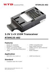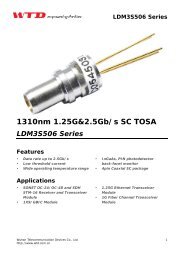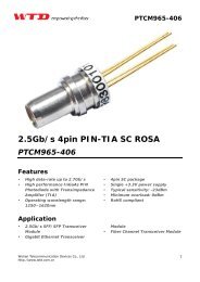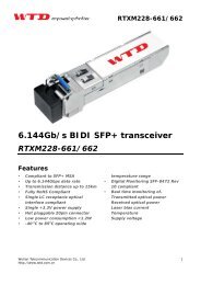
2.5G SFP transceiver module with DDM function RTXM192-404
2.5G SFP transceiver module with DDM function RTXM192-404
2.5G SFP transceiver module with DDM function RTXM192-404
- No tags were found...

You also want an ePaper? Increase the reach of your titles
YUMPU automatically turns print PDFs into web optimized ePapers that Google loves.
<strong>RTXM192</strong>-<strong>404</strong>111 1 Reserved Set to 0.111 0 Reserved Set to 0.Each of the measured values has a corresponding high alarm, low alarm, high warning and low warningthreshold level at location 00-39(x0A2) written as the data format of a corresponding valued shown in Table3.3.Alarm and warning flags at bytes 112-119(0xA2) are defined as follows.Alarm flags indicate conditions likely to result (or have resulted) in link failure and cause for immediate action.Warning flags indicate conditions outside the guaranteed operating specification of <strong>transceiver</strong> but notnecessarily causes of immediate link failures.Table 3.3 Alarm and Warning FlagsByte Bit(s) NameDescription112 7 Temperature High Alarm Set when temperature monitor value exceeds high alarm level.112 6 Temperature Low Alarm Set when temperature monitor value exceeds low alarm level.112 5 Vcc High Alarm Set when Vcc monitor value exceeds high alarm level.112 4 Vcc Low Alarm Set when Vcc monitor value exceeds Low alarm level.112 3 Laser Bias High Alarm Set when laser bias monitor value exceeds high alarm level.112 2 Laser Bias Low Alarm Set when laser bias monitor value exceeds low alarm level.112 1 Tx Power High Alarm Set when Tx power monitor value exceeds high alarm level112 0 Tx Power Low Alarm Set when Tx power monitor value exceeds low alarm level.113 7 Rx Power High Alarm Set when Rx power monitor value exceeds high alarm level113 6 Rx Power Low Alarm Set when Rx power monitor value exceeds low alarm level113 5-0 Reserved All bits set to 0.114 7-0 Reserved All bits set to 0.115 7-0 Reserved All bits set to 0.116 7 Temperature High warning Set when temperature monitor value exceeds high warning level.116 6 Temperature Low warning Set when temperature monitor value exceeds low warning level.116 5 Vcc High warning Set when Vcc monitor value exceeds high warning level.116 4 Vcc Low warning Set when Vcc monitor value exceeds Low warning level.116 3 Laser Bias High warning Set when laser bias monitor value exceeds high warning level.116 2 Laser Bias Low warning Set when laser bias monitor value exceeds low warning level.116 1 Tx Power High warning Set when Tx power monitor value exceeds high warning level116 0 Tx Power Low warning Set when Tx power monitor value exceeds low warning level.117 7 Rx Power High warning Set when Rx power monitor value exceeds high warning level117 6 Rx Power Low warning Set when Rx power monitor value exceeds low warning level117 5-0 Reserved All bits set to 0.118 7-0 Reserved All bits set to 0.119 7-0 Reserved All bits set to 0.Wuhan Telecommunication Devices Co., Ltd.http://www.wtd.com.cn8
<strong>RTXM192</strong>-<strong>404</strong>Pin Description20VeeT1VeeT19TD-2Tx_Fault18TD+3Tx_disable17VeeT4MOD-DEF(2)16VccT5MOD-DEF(1)15VccR6MOD-DEF(0)14VeeR7Rate Select13RD+8LOS12RD-9VeeR11VeeR10VeeRTop of BoardBottom of BoardAs Viewed Through Top of BoardPin Name Function/Description Engagement order Notes1 VeeT Transmitter Ground 12 TX Fault Transmitter Fault Indication 3 13 TX Disable Transmitter Disable-Module disables on high or open 3 24 MOD-DEF2 Module Definition 2-Two wire serial ID interface 3 35 MOD-DEF1 Module Definition 1-Two wire serial ID interface 3 36 MOD-DEF0 Module Definition 0-Two wire serial ID interface 3 37 Rate Select Not Connected 38 LOS Loss of Signal 3 49 VeeR Receiver Ground 110 VeeR Receiver Ground 111 Veer Receiver Ground 112 RD- Inverse Received Data out 3 513 RD+ Received Data out 3 514 VeeR Receiver Ground 115 VccR Receiver Power ---- +3.3V±5% 2 616 VccT Transmitter Power ---- +3.3 V±5% 2 617 VeeT Transmitter Ground 118 TD+ Transmitter Data In 3 719 TD- Inverse Transmitter Data In 3 720 VeeT Transmitter Ground 1Note1. TX Fault is open collector/drain output which should be pulled up externally <strong>with</strong> a 4.7K – 10KΩresistor on the host board to supply
<strong>RTXM192</strong>-<strong>404</strong>of some kind. Low indicates normal operation. In the low state, the output will be pulled to
<strong>RTXM192</strong>-<strong>404</strong>Required Host Board ComponentsThe MSA power supply noise rejection filter is required on the host PCB to meet data sheet performance. TheMSA filter incorporates an inductor which should be rated 400mA DC and 1Ωserial resistance or better. Itshould not be replaced <strong>with</strong> a ferrite. The required filter is illustrated in Figure 3. The MSA also specifies that4.7K to 10KΩ pull-up resistors for TX_FAULT, LOS, and MOD_DEF0,1,2 are required on the host PCB. Figureis the suggested <strong>transceiver</strong>/host interface.Typical application circuitLaserDriverReceiverAmplifierWuhan Telecommunication Devices Co., Ltd.http://www.wtd.com.cn11
<strong>RTXM192</strong>-<strong>404</strong>Package outlinemaxPCB layout recommendationWuhan Telecommunication Devices Co., Ltd.http://www.wtd.com.cn12
<strong>RTXM192</strong>-<strong>404</strong>Regulatory ComplianceFeature Test Method PerformanceElectrostatic Discharge MIL-STD-883E(ESD) to the Electrical Pins Method 3015.7Class 1 (>1.5kV) – Human Body ModelElectrostatic(ESD) ImmunityDischargeIEC61000-4-2Class 2(>4.0kV)CISPR22 ITEClass BElectromagnetic Interference FCC Class BCompliant <strong>with</strong> standard(EMI)CENELECEN55022VCCI Class 1Typically show no measurable effect from a 3 V/m field sweptIEC61000-4-3Immunityfrom 80 to 1000MHz applied to the <strong>transceiver</strong> <strong>with</strong>out aClass 2chassis enclosure.FDA 0322110-00SafetyCDRH 21-CFR 1040 Class 1UL E239070TUV R50111660 0001CE E8 0501 54481 004Wuhan Telecommunication Devices Co., Ltd.http://www.wtd.com.cn13
<strong>RTXM192</strong>-<strong>404</strong>Ordering InformationPart No.<strong>RTXM192</strong>-<strong>404</strong> <strong>SFP</strong>Package Datarate<strong>2.5G</strong> 1310nmFPSpecificationLaser Power Detector Sensitivity Temp Reach Other-10 ~-3dBmPIN< -18dBm -40~85oC 2km<strong>DDM</strong>,RoHSApplicationCodeSDH I-16WTD reserves the right to make changes to the product(s) or information contained herein <strong>with</strong>out notice. Noliability is assumed as a result of their use or application. No rights under any patent accompany the sale ofany such product(s) or information.Edition 2009-12-01Published by Wuhan Telecommunication Devices Co.,Ltd.Copyright © WTDAll Rights Reserved.Wuhan Telecommunication Devices Co., Ltd.http://www.wtd.com.cn14