RTXM228-661/662
RTXM228-661/662
RTXM228-661/662

You also want an ePaper? Increase the reach of your titles
YUMPU automatically turns print PDFs into web optimized ePapers that Google loves.
Wuhan Telecommunication Devices Co., Ltd.<br />
http://www.wtd.com.cn<br />
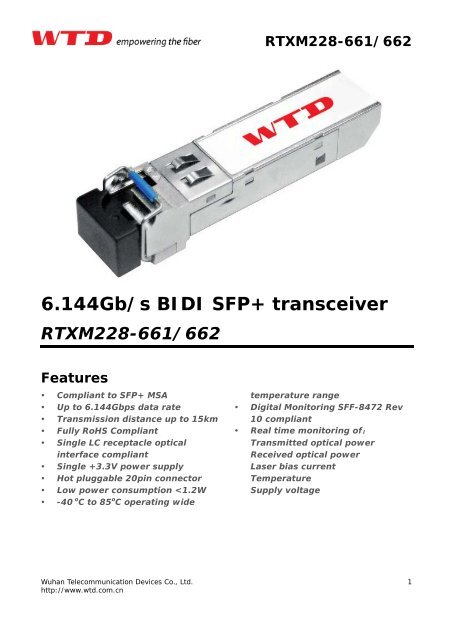
<strong>RTXM228</strong>-<strong>661</strong>/<strong>662</strong><br />
6.144Gb/s BIDI SFP+ transceiver<br />
<strong>RTXM228</strong>-<strong>661</strong>/<strong>662</strong><br />
Features<br />
� Compliant to SFP+ MSA<br />
� Up to 6.144Gbps data rate<br />
� Transmission distance up to 15km<br />
� Fully RoHS Compliant<br />
� Single LC receptacle optical<br />
interface compliant<br />
� Single +3.3V power supply<br />
� Hot pluggable 20pin connector<br />
� Low power consumption
Application<br />
� Wireless and cellular base station system interconnect:<br />
OBSAI rates 3.072 Gb/s, 6.144Gb/s<br />
CPRI rates 2.4576 Gb/s, 4.9152Gb/s, 6.144Gb/s<br />
� 2G/4G FC Data Storage<br />
Standards<br />
� SFF-8431 Rev 2.0<br />
� SFF-8472 Rev 10.2<br />
Absolute Maximum Ratings<br />
Wuhan Telecommunication Devices Co., Ltd.<br />
http://www.wtd.com.cn<br />
<strong>RTXM228</strong>-<strong>661</strong>/<strong>662</strong><br />
Parameter Symbol Unit Min Max<br />
Storage Temperature Range Ts<br />
o C -40 +85<br />
Relative Humidity RH % 5 95<br />
Power Supply Voltage Vcc V -0.3 +4<br />
Recommended Operating Conditions<br />
Parameter Symbol Unit Min Typ Max<br />
Operating Case Temperature Range Tc<br />
o C -40 85<br />
Power Supply Voltage Vcc V 3.13 3.3 3.46<br />
Bit Rate BR Gb/s 2.4576 6.144<br />
Bit Error Ratio BER 10 -12<br />
Max Supported Link Length L Km 15<br />
Electrical Characteristics (Tc= -40~85 o<br />
C and Vcc= 3.14 to 3.46)<br />
Parameter<br />
Symbol Unit Min Typ Max Notes<br />
Supply Voltage VCC V 3.14 3.3 3.46<br />
Supply Current Icc mA 345<br />
Power Consumption Pc W 1.2<br />
Transmitter<br />
Input Differential Impedance RIN Ω 80 100 120<br />
Differential Data Input Swing VIN mVp-p 180 700<br />
Transmit Disable Voltage VDIS V 2 V CCHOST<br />
Transmit Enable Voltage VEN V V EE VEE +0.8<br />
Transmit Fault Assert Voltage VFA V 2.2 V CCHOST<br />
2
Wuhan Telecommunication Devices Co., Ltd.<br />
http://www.wtd.com.cn<br />
<strong>RTXM228</strong>-<strong>661</strong>/<strong>662</strong><br />
Transmit Fault De-Assert Voltage VFDA Receiver<br />
V V EE VEE +0.4<br />
Differential Data Output Swing VOD mVp-p 450 600 850<br />
Output Rise Time tRISE pS<br />
60<br />
Output Fall Time tFALL pS<br />
60<br />
LOS Fault VLOSFT V 2 V CCHOST<br />
LOS Normal VLOSNR V V EE VEE +0.8<br />
Optical Characteristics (Tc= -40~85 o<br />
C and Vcc= 3.14 to 3.46)<br />
Parameter<br />
Symbol Unit Min Typ Max Notes<br />
Transmitter<br />
Average output power Po dBm -8.4 +0.5 1<br />
Center Wavelength λc nm<br />
Extinction Ratio EX dB 3.5<br />
1263 1277<br />
1323 1337<br />
Spectral Width (-20dB) ∆λ nm 1 3<br />
SMSR dB 30<br />
Relative Intensity Noise RIN dB/Hz -128<br />
Laser Off Power POFF dBm -35<br />
Link Power Budget dB 9.4 4,5<br />
Receiver<br />
Center Wavelength λc nm<br />
1263 1277<br />
1323 1337<br />
Receiver Sensitivity (OMA) R SENSE1 dBm -13.8 2<br />
Overload Input Optical Power Pover dBm +0.5 2<br />
Receiver Reflectance RREFL dB<br />
-12<br />
LOS Assert LOS LOSD dBm -30<br />
LOS De-Assert LOS LOSA dBm<br />
-15<br />
LOS Hysteresis dB 0.5<br />
Note 1: Minimum output optical level is at end of life<br />
Note 2: Sensitivity for PRBS 2 7<br />
-1 and BER better than or equal to 10E-12<br />
Note 3: Spectral width has to be defined over -20dBm<br />
Note 4: Budget numbers are rounded to nearest 0.1 dB<br />
Note 5: Link penalties are used for link budget calculations. They are not requirements and are not meant to<br />
be tested.<br />
3
Pin function definitions<br />
Wuhan Telecommunication Devices Co., Ltd.<br />
http://www.wtd.com.cn<br />
Figure 2: Pin function definitions<br />
Table 1: Transceiver pin descriptions<br />
<strong>RTXM228</strong>-<strong>661</strong>/<strong>662</strong><br />
Pin Number Symbol Name Description<br />
1,17,20 VeeT Transmitter Signal Ground<br />
2 TX Fault Transmitter Fault Out (OC)<br />
3 TX Disable Transmitter Disable In (LVTTL)<br />
4 SDA<br />
5 SCL<br />
6 MOD-ABS<br />
7 RS0<br />
9 RS1<br />
Module Definition Identifiers<br />
Receiver Rate Select (LVTTL)<br />
Transmitter Rate Select (LVTTL)<br />
8 LOS Loss of Signal Out (OC)<br />
These pins should be connected to signal<br />
ground on the host board.<br />
Logic “1” Output = Laser Fault (Laser off<br />
before t_fault)<br />
Logic “0” Output = Normal Operation<br />
This pin is open collector compatible, and<br />
should be pulled up to Host Vcc with a 10kΩ<br />
resistor.<br />
Logic “1” Input (or no connection) = Laser<br />
off<br />
Logic “0” Input = Laser on<br />
This pin is internally pulled up to VccT with a<br />
10 kΩ resistor.<br />
Serial ID with SFF 8472 Diagnostics<br />
Module Definition pins should be pulled up<br />
to Host Vcc with 10 kΩ resistors.<br />
These pins have an internal 33kΩ pull-down<br />
to ground. A signal on either of these pins<br />
will not affect module performance.<br />
Sufficient optical signal for potential<br />
BER < 1x10<br />
4<br />
-12<br />
= Logic “0”<br />
Insufficient optical signal for potential
10,11,14 VeeR Receiver Signal Ground<br />
12 RD-<br />
13 RD+<br />
Wuhan Telecommunication Devices Co., Ltd.<br />
http://www.wtd.com.cn<br />
Receiver Negative DATA Out<br />
(CML)<br />
Receiver Positive DATA Out<br />
(CML)<br />
15 VccR Receiver Power Supply<br />
16 VccT Transmitter Power Supply<br />
18 TD+<br />
19 TD-<br />
Transmitter Positive DATA In<br />
(CML)<br />
Transmitter Negative DATA In<br />
(CML)<br />
Typical application circuit<br />
+3.3V<br />
0.1uF<br />
C<br />
0.1uF<br />
C<br />
RD-<br />
RD+<br />
L<br />
4.7uH<br />
TD+<br />
TD-<br />
L<br />
4.7uH<br />
C<br />
22uF<br />
C<br />
22uF<br />
11<br />
GNDR12<br />
13<br />
14<br />
C<br />
0.1uF GNDR15<br />
16<br />
C 17<br />
0.1uF<br />
GNDT18<br />
19<br />
GNDT<br />
20<br />
<strong>RTXM228</strong>-<strong>661</strong>/<strong>662</strong><br />
BER < 1x10 -12<br />
= Logic “1”<br />
This pin is open collector compatible, and<br />
should be pulled up to Host Vcc with a 10kΩ<br />
resistor.<br />
SDA<br />
TX_DISABLE<br />
3<br />
TX_FAULT<br />
2<br />
VEET<br />
1<br />
4<br />
VEER<br />
VEER<br />
10<br />
RD-<br />
RS1<br />
9 GNDR<br />
RD+<br />
RX_LOS<br />
8<br />
VEER<br />
RS0<br />
7<br />
VCCR MOD_ABS<br />
6<br />
VCCT<br />
SCL<br />
5<br />
VEET<br />
TD+<br />
TD-<br />
VEET<br />
GNDT<br />
SFP+ MODULE<br />
Figure 3: Typical application schematics<br />
These pins should be connected to signal<br />
ground on the host board.<br />
Light on = Logic “0” Output Receiver DATA<br />
output is internally AC coupled and series<br />
terminated with a 50Ω resistor.<br />
Light on = Logic “1” Output Receiver DATA<br />
output is internally AC coupled and series<br />
terminated with a 50Ω resistor.<br />
This pin should be connected to a filtered<br />
+3.3V power supply on the host board. See<br />
Figure 3.Recommended power supply filter<br />
This pin should be connected to a filtered<br />
+3.3V power supply on the host board. See<br />
Figure 3.Recommended power supply filter<br />
Logic “1” Input = Light on Transmitter DATA<br />
inputs are internally AC coupled and<br />
terminated with a differential 100Ω resistor.<br />
Logic “0” Input = Light on Transmitter DATA<br />
inputs are internally AC coupled and<br />
terminated with a differential 100Ω resistor.<br />
+3.3V<br />
R R R R<br />
R<br />
4.7-10K x 5<br />
RS1<br />
RX-LOS<br />
RS0<br />
MOD-ABS<br />
SCL<br />
SDA<br />
TX-DIS<br />
TX-FAULT<br />
5
Electrostatic Discharge (ESD)<br />
Wuhan Telecommunication Devices Co., Ltd.<br />
http://www.wtd.com.cn<br />
<strong>RTXM228</strong>-<strong>661</strong>/<strong>662</strong><br />
The <strong>RTXM228</strong> is compatible with ESD levels found in typical manufacturing and operating environments as<br />
described in Table 2. In the normal handling and operation of optical transceivers, ESD is of concern in two<br />
circumstances.<br />
The first case is during handling of the transceiver prior to insertion into an SFP+ compliant cage. To protect<br />
the device, it’s important to use normal ESD handling pre-cautions. These include use of grounded wrist<br />
straps, work-benches and floor wherever a transceiver is handled.<br />
The second case to consider is static discharges to the exterior of the host equipment chassis after installation.<br />
If the optical interface is exposed to the exterior of host equipment cabinet, the transceiver may be subject<br />
to system level ESD requirements.<br />
Electromagnetic Interference (EMI)<br />
Equipment incorporating gigabit transceivers is typically subject to regulation by the FCC in the United States,<br />
CENELEC EN55022 (CISPR 22) in Europe and VCCI in Japan. The <strong>RTXM228</strong> compliance to these standards is<br />
detailed in Table 2. The metal housing and shielded design of the <strong>RTXM228</strong> minimizes the EMI challenge<br />
facing the equipment designer.<br />
EMI Immunity (Susceptibility)<br />
Due to its shielded design, the EMI immunity of the <strong>RTXM228</strong> exceeds typical industry standards.<br />
Table 2: Regulatory compliance<br />
Feature Test Method Performance<br />
Electrostatic Discharge (ESD) to the<br />
Electrical Pins<br />
Electrostatic Discharge (ESD) to the<br />
Duplex LC Receptacle<br />
Electromagnetic Interference (EMI)<br />
Immunity<br />
RoHS Compliance<br />
MIL-STD-883C Method 3015.4 Class 1 (> 1500 Volts)<br />
Variation of IEC 61000-4-2<br />
CISPR22 ITE Class B<br />
EN55022 Class B<br />
IEC61000-4-3 Class 2<br />
EN55024<br />
Typically, no damage occurs with 15<br />
kV when the duplex LC connector<br />
receptacle is contacted by a Human<br />
Body Model probe.<br />
Compliant with standards<br />
Typically show no measurable effect<br />
from a 3V/m field swept from 80 to<br />
1000MHz applied to the transceiver<br />
without a chassis enclosure.<br />
Less than 1000 ppm of cadmium,<br />
lead, mercury, hexavalent<br />
chromium, polybrominated<br />
biphenyls, and polybrominated<br />
biphenyl ethers.<br />
6
Digital Diagnostic Interface Definition<br />
<strong>RTXM228</strong>-<strong>661</strong>/<strong>662</strong><br />
The 2-wire serial interface addresses of the SFP+ module are 1010000x (A0h) and 1010001x (A2h). Shown<br />
in Figure 4.<br />
Figure 4: Digital Diagnostic Memory Map<br />
Accessing Serial ID Memory uses the 2 wire address 1010000X (A0). Memory Contents of Serial ID are shown<br />
in Table 3.<br />
Data Size<br />
Address (Bytes)<br />
Table 3: Serial ID Memory Contents<br />
Name of Field Contents(Hex) Description<br />
0 1 Identifier<br />
BASE ID FIELDS<br />
03 SFP+<br />
1 1 Ext. Identifier 04 SFP function is defined by serial ID only<br />
2 1 Connector 07 LC Connector<br />
3-10 8 Transceiver Transceiver Codes<br />
11 1 Encoding 03 NRZ<br />
12 1 BR, Nominal 3D 6.144Gbit/s<br />
13 1 Reserved<br />
14 1 Length (9μm) km 0F<br />
15 1 Length (9μm) 100m 00<br />
Transceiver transmit distance<br />
16 1 Length (50μm) 10m 00<br />
15km<br />
17 1 Length(62.5μm)10m 00<br />
18 1 Length (Copper) 00 Not compliant<br />
19 1 Reserved<br />
20-35 16 Vendor name<br />
57 54 44 20 20 20 20 20<br />
20 20 20 20 20 20 20 20<br />
“WTD”(ASCII)<br />
36 1 Reserved<br />
37-39 3 Vendor OUI 00 1C AD<br />
40-55 16 Vendor PN Transceiver part number<br />
56-59 4 Vendor rev 20 20 20 20<br />
Wuhan Telecommunication Devices Co., Ltd.<br />
http://www.wtd.com.cn<br />
7
Wuhan Telecommunication Devices Co., Ltd.<br />
http://www.wtd.com.cn<br />
<strong>RTXM228</strong>-<strong>661</strong>/<strong>662</strong><br />
60-61 2 Wavelength Transceiver wavelength<br />
62 1 Reserved<br />
63 1 CC_BASE Check Sum (Variable) Check code for Base ID Fields<br />
EXTENDED ID FIELDS<br />
64-65 2 Options 00 1A<br />
66 1 BR,max 00<br />
67 1 BR,min 00<br />
68-83 16 Vendor SN<br />
TX_DISABLE, TX_FAULT and Loss of<br />
Signal implemented.<br />
42 30 30 39 38 32 32 20 Serial Number of transceiver (ASCII). For<br />
20 20 20 20 20 20 20 20<br />
84-91 8 Date code 30 32 31 30 30 35 20 20<br />
92 1<br />
Diagnostic<br />
Monitoring Type<br />
93 1 Enhanced Options F6<br />
94 1<br />
SFF_8472<br />
Compliance<br />
68<br />
03<br />
example “B009822”.<br />
Manufactory date code. For example<br />
“021005”.<br />
Digital diagnostic monitoring<br />
implemented, “internal calibrated” is<br />
implemented, RX measurement type is<br />
Average Power.<br />
Optional Alarm/Warning flags<br />
implemented for all monitored quantities,<br />
Optional Soft TX_FAULT monitoring<br />
implemented, Optional Soft RX_LOS<br />
monitoring implemented.<br />
Includes functionality described in<br />
Rev10.2 SFF-8472.<br />
95 1 CC_EXT Check Sum (Variable) Check sum for Extended ID Field.<br />
VENDOR SPECIFIC ID FIELDS<br />
96-127 32 Vendor Specific Read only Depends on customer information<br />
128-255 128 Reserved Read only<br />
Diagnostic Monitor Functions<br />
Diagnostic Monitor Functions interface uses the 2 wire address 1010001X (A2). Memory contents of<br />
Diagnostic Monitor Functions are shown in Table 4<br />
Table 4: Memory contents of Diagnostic Monitor Function<br />
Data Address Field Size (bytes) Name Contents and Description<br />
00-01 2<br />
Alarm and Warning Thresholds<br />
Temperature High Alarm<br />
02-03 2 Temperature Low Alarm<br />
04-05 2 Temperature High Warning<br />
06-07 2 Temperature Low Warning<br />
08-09 2 Vcc High Alarm<br />
10-11 2 Vcc Low Alarm<br />
12-13 2 Vcc High Warning<br />
8
14-15 2 Vcc Low Warning<br />
16-17 2 Bias High Alarm<br />
18-19 2 Bias Low Alarm<br />
20-21 2 Bias High Warning<br />
22-23 2 Bias Low Warning<br />
24-25 2 TX Power High Alarm<br />
26-27 2 TX Power Low Alarm<br />
28-29 2 TX Power High Warning<br />
30-31 2 TX Power Low Warning<br />
32-33 2 RX Power High Alarm<br />
34-35 2 RX Power Low Alarm<br />
36-37 2 RX Power High Warning<br />
38-39 2 RX Power Low Warning<br />
40-55 16 Reserved<br />
Wuhan Telecommunication Devices Co., Ltd.<br />
http://www.wtd.com.cn<br />
Calibration Constants<br />
<strong>RTXM228</strong>-<strong>661</strong>/<strong>662</strong><br />
56-59 4 RX Power Calibration Data4 00 00 00 00<br />
60-63 4 RX Power Calibration Data3<br />
00 00 00 00<br />
64-67 4 RX Power Calibration Data2 00 00 00 00<br />
68-71 4 RX Power Calibration Data1<br />
72-75 4 RX Power Calibration Data0<br />
3F 80 00 00<br />
00 00 00 00<br />
76-77 2 Bias Calibration Data1 01 00<br />
78-79 2 Bias Calibration Data0 00 00<br />
80-81 2 TX Power Calibration Data1 01 00<br />
82-83 2 TX Power Calibration Data0 00 00<br />
84-85 2 Temperature Calibration Data1 01 00<br />
86-87 2 Temperature Calibration Data0 00 00<br />
88-89 2 Vcc Calibration Data1 01 00<br />
90-91 2 Vcc Calibration Data0 00 00<br />
92-94 3 Reserved<br />
95 1 Check Sum<br />
Real Time Diagnostic Monitor Interface<br />
96-97 2 Measured Temperature<br />
98-99 2 Measured Vcc<br />
100-101 2 Measured Bias<br />
102-103 2 Measured TX Power<br />
104-105 2 Measured RX Power<br />
106-109 4 Reserved<br />
110 1 Logic Status<br />
111 1 AD Conversion Updates<br />
112-119 8 Alarm and Warning Flags<br />
Vendor Specific<br />
120-127 8 Vendor Specific<br />
9
128-247 120 User writable EEPROM<br />
248-255 8 Vendor Specific<br />
Transceiver Timing Characteristics<br />
(Tc=-40 o C to 85 o<br />
C and VccT, VccR = 3.145 to 3.465)<br />
Parameter<br />
Wuhan Telecommunication Devices Co., Ltd.<br />
http://www.wtd.com.cn<br />
<strong>RTXM228</strong>-<strong>661</strong>/<strong>662</strong><br />
Symbol Minimum Maximum Unit Notes<br />
Hardware TX_DISABLE Assert Time t_off 10 μs 1<br />
Hardware TX_DISABLE Negate Time t_on 1 ms 2<br />
Time to initialize including reset of TX_FAULT t_init 300 ms 3<br />
Hardware TX_FAULT Assert Time t_fault 100 μs 4<br />
Hardware TX_DISABLE to Reset t_reset 10 μs 5<br />
Hardware RX_LOS DeAssert Time t_loss_on 100 μs 6<br />
Hardware RX_LOS Assert Time t_loss_off 100 μs 7<br />
Software TX_DISABLE Assert Time t_off_soft 100 ms 8<br />
Software TX_DISABLE Negate Time t_on_soft 100 ms 9<br />
Software Tx_FAULT Assert Time t_fault_soft 100 ms 10<br />
Software Rx_LOS Assert Time t_loss_on_soft 100 ms 11<br />
Software Rx_LOS De-Assert Time t_loss_off_soft 100 ms 12<br />
Analog parameter data ready t_data 1000 ms 13<br />
Serial bus hardware ready t_serial 300 ms 14<br />
Write Cycle Time t_write 10 ms 15<br />
Serial ID Clock Rate f_serial_clock 400 kHz<br />
Note 1: Time from rising edge of TX_DISABLE to when the optical output falls below 10% of nominal.<br />
Note 2: Time from falling edge of TX_DISABLE to when the modulated optical output rises above 90% of<br />
nominal.<br />
Note 3: Time from power on or falling edge of Tx_Disable to when the modulated optical output rises above<br />
90% of nominal.<br />
Note 4: From power on or negation of TX_FAULT using TX_DISABLE.<br />
Note 5: Time TX_DISABLE must be held high to reset the laser fault shutdown circuitry.<br />
Note 6: Time from loss of optical signal to Rx_LOS Assertion.<br />
Note 7: Time from valid optical signal to Rx_LOS De-Assertion.<br />
Note 8: Time from two-wire interface assertion of TX_DISABLE (A2h, byte 110, bit 6) to when the optical<br />
output falls below 10% of nominal. Measured from falling clock edge after stop bit of write transaction.<br />
Note 9: Time from two-wire interface de-assertion of TX_DISABLE (A2h, byte 110, bit 6) to when the<br />
modulated optical output rises above 90% of nominal.<br />
Note 10: Time from fault to two-wire interface TX_FAULT (A2h, byte 110, bit 2) asserted.<br />
Note 11: Time for two-wire interface assertion of Rx_LOS (A2h, byte 110, bit 1) from loss of optical signal.<br />
Note 12: Time for two-wire interface de-assertion of Rx_LOS (A2h, byte 110, bit 1) from presence of valid<br />
optical signal.<br />
Note 13: From power on to data ready bit asserted (A2h, byte 110, bit 0). Data ready indicates analog<br />
10
monitoring circuitry is functional.<br />
Wuhan Telecommunication Devices Co., Ltd.<br />
http://www.wtd.com.cn<br />
<strong>RTXM228</strong>-<strong>661</strong>/<strong>662</strong><br />
Note 14: Time from power on until module is ready for data transmission over the serial bus (reads or writes<br />
over A0h and A2h).<br />
Note 15: Time from stop bit to completion of a 1-8 byte write command.<br />
Package outline(Unit: mm)<br />
Ordering Information<br />
Part No<br />
Package Data rate Laser<br />
Specifications<br />
Optical<br />
Power<br />
<strong>RTXM228</strong>-<strong>661</strong> SFP+ 2.4576~6.144 1270nm -8.4 1330nm<br />
Gb/s DFB ~+0.5dBm PIN<br />
<strong>RTXM228</strong>-<strong>662</strong> SFP+ 2.4576~6.144 1330nm -8.4 1270nm<br />
Gb/s DFB ~+0.5dBm PIN<br />
Sensitivity<br />
Detector<br />
OMA<br />
Wuhan Telecommunication Devices Co., Ltd.<br />
http://www.wtd.com.cn<br />
<strong>RTXM228</strong>-<strong>661</strong>/<strong>662</strong><br />
WTD reserves the right to make changes to the product(s) or information contained herein without notice. No<br />
liability is assumed as a result of their use or application. No rights under any patent accompany the sale of<br />
any such product(s) or information.<br />
Edition 2010-7-2<br />
Published by Wuhan Telecommunication Devices Co.,Ltd.<br />
Copyright © WTD<br />
All Rights Reserved.<br />
12