RTXM228-661/662
RTXM228-661/662
RTXM228-661/662

You also want an ePaper? Increase the reach of your titles
YUMPU automatically turns print PDFs into web optimized ePapers that Google loves.
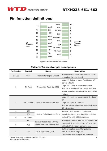
Pin function definitions<br />
Wuhan Telecommunication Devices Co., Ltd.<br />
http://www.wtd.com.cn<br />
Figure 2: Pin function definitions<br />
Table 1: Transceiver pin descriptions<br />
<strong>RTXM228</strong>-<strong>661</strong>/<strong>662</strong><br />
Pin Number Symbol Name Description<br />
1,17,20 VeeT Transmitter Signal Ground<br />
2 TX Fault Transmitter Fault Out (OC)<br />
3 TX Disable Transmitter Disable In (LVTTL)<br />
4 SDA<br />
5 SCL<br />
6 MOD-ABS<br />
7 RS0<br />
9 RS1<br />
Module Definition Identifiers<br />
Receiver Rate Select (LVTTL)<br />
Transmitter Rate Select (LVTTL)<br />
8 LOS Loss of Signal Out (OC)<br />
These pins should be connected to signal<br />
ground on the host board.<br />
Logic “1” Output = Laser Fault (Laser off<br />
before t_fault)<br />
Logic “0” Output = Normal Operation<br />
This pin is open collector compatible, and<br />
should be pulled up to Host Vcc with a 10kΩ<br />
resistor.<br />
Logic “1” Input (or no connection) = Laser<br />
off<br />
Logic “0” Input = Laser on<br />
This pin is internally pulled up to VccT with a<br />
10 kΩ resistor.<br />
Serial ID with SFF 8472 Diagnostics<br />
Module Definition pins should be pulled up<br />
to Host Vcc with 10 kΩ resistors.<br />
These pins have an internal 33kΩ pull-down<br />
to ground. A signal on either of these pins<br />
will not affect module performance.<br />
Sufficient optical signal for potential<br />
BER < 1x10<br />
4<br />
-12<br />
= Logic “0”<br />
Insufficient optical signal for potential