kerf-free wafering - Avsusergroups.org
kerf-free wafering - Avsusergroups.org
kerf-free wafering - Avsusergroups.org

Create successful ePaper yourself
Turn your PDF publications into a flip-book with our unique Google optimized e-Paper software.
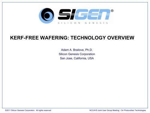
KERF-FREE WAFERING: TECHNOLOGY OVERVIEWAdam A. Brailove, Ph.D.Silicon Genesis CorporationSan Jose, California, USA©2011 Silicon Genesis Corporation. All rights reserved NCCAVS Joint User Group Meeting - On Photovoltaic Technologies
Outline• About Silicon Genesis (SiGen)• PV Market and Limits of Current Technology• PolyMax Kerf-less Wafering Technology• Manufacturing Equipment• Material Characteristics of PolyMax• Conclusions©2011 Silicon Genesis Corporation. All rights reserved NCCAVS Joint User Group Meeting - On Photovoltaic Technologies
About Silicon Genesis• Founded in 1997• Developed Layer-Transfer process and manufacturingequipment for semiconductor (SOI) and optoelectronic/displaymarkets (SOQ)• Recently focused technology on developing PolyMax TMsystem for solar <strong>wafering</strong>Plasma-BondSystemCleave System150mm Silicon-On-Quartz300mm 100nm SOI©2011 Silicon Genesis Corporation. All rights reserved NCCAVS Joint User Group Meeting - On Photovoltaic Technologies
Increasing Demand – PV EquipmentSolar installations are expected to continue to growby 28% over the next five years― This increase will continue driving demand forsolar <strong>wafering</strong> equipment• Wafer capacity expected to expand by5GW – 7.5GW per year for the next threeyears― Federal RPS legislation is expected to increasedemand for solar energyWorldwide PV Market Size (Installed)Crystalline silicon is the dominant solar technologyrepresenting ~90% of the market― Achieve higher efficiencies from 15% to 20%+― Lower risks and therefore higher bankability― Thin film technology, though having an attractivecost structure, faces efficiency and scalingchallenges― Alternative solar technologies are many years awayfrom gaining any significant market shareSource: Solar Vision Consulting, EUPD Research, Navigant, Photon International.©2011 Silicon Genesis Corporation. All rights reserved NCCAVS Joint User Group Meeting - On Photovoltaic Technologies
c-Si PV Value ChainPoly SiGluingIngotSawingWaferPre-CleaningSingulationCellCleaningModuleInspection©2011 Silicon Genesis Corporation. All rights reserved NCCAVS Joint User Group Meeting - On Photovoltaic Technologies
Wafering: Multi-Wire SawingMeyer Burger DS 271 Wire Saw• Multiple parallel finesteel wires drawn acrossingot at high speed• SiC abrasive slurryentrained• Slowly abrades throughsiliconSource: Photon International©2011 Silicon Genesis Corporation. All rights reserved NCCAVS Joint User Group Meeting - On Photovoltaic Technologies
Limits of Wire-Saw Technology• Cost• Kerf-loss currently consumes > 50% of polysilicon• Silicon is turned into ‘sawdust’ mixed with abrasive slurry• Silicon recovery from slurry is costly, complex• Cost of wire, slurry and slurry production/recycle facility• Cost of ingot puller capacity to produce silicon lost to <strong>kerf</strong>• Cost of wafer washing and wet singulation• Wafer Thickness Reduction• Need thinner wafers & more efficient silicon usage• Sawing is a rough mechanical process• Obviously not well suited for micron scale layers of silicon• Industry encountering difficulty scaling down wire-sawn wafer thickness• Saw damage/micro-cracks increases probability of wafer breakage• Tradeoff: thinner = slower cutting speed• Thickness variation, wafer to wafer variability wafer binning• No roadmap to < 100 micron thicknesses©2011 Silicon Genesis Corporation. All rights reserved NCCAVS Joint User Group Meeting - On Photovoltaic Technologies
SiGen’s Novel Solution: PolyMaxIon ImplantationInitiation and PropagationCleaved Wafer20-150μm• A two-step process:1. Implant light ions into c-Si shaped brick• Form sub-surface cleave layer• Implant small initiation area with higher dose2. Controlled Cleave with energy beam• Initiate cleave in high dose area• Propagate crack across brick area to release wafer• Repeat on newly exposed brick surface©2011 Silicon Genesis Corporation. All rights reserved NCCAVS Joint User Group Meeting - On Photovoltaic Technologies
Proton Range in Silicon• ‘Range’ = averageproton depth• Proton energy setswafer thickness• ‘Straggle’ =variation in depth• Straggle scalesdown with lowerenergies, thinnerwafers.©2011 Silicon Genesis Corporation. All rights reserved NCCAVS Joint User Group Meeting - On Photovoltaic Technologies
PolyMax Wafers and Foils20μm50μm150μm• Demonstrated <strong>kerf</strong>-less <strong>wafering</strong>• Wide range of wafer thickness produced• Proton energies: 1.1-4 MeV• 20, 50, 85, 120, 150 microns• 125 mm and 156 mm pseudo-squares• High R&D yields• No apparent problems due toprogressive slicing• crystalline silicon©2011 Silicon Genesis Corporation. All rights reserved NCCAVS Joint User Group Meeting - On Photovoltaic Technologies
PolyMax SEM & AFM ResultsX 5.00 μm/divZ 1000.00 nm/divPolyMax TM 20μm thick waferRMS 59.1nmZ range: 493.1nmX 5.00 μm/divZ 1000.00 nm/divPolyMax TM 50μm thick waferRMS 97.6nmZ range: 796.3nmX 10.00 μm/divZ 2000.00 nm/divPolyMax TM 150μm thick waferRMS 386.8nmZ range: 3.2μm• Roughness scalesdown with thinnerwafers• Scaling is visuallyobservable withnaked eye• SEM and AFMconfirm• No microscratchesas insawn wafers.20um 50um 150um©2011 Silicon Genesis Corporation. All rights reserved NCCAVS Joint User Group Meeting - On Photovoltaic Technologies
Wafer Thickness• Wafer thicknessdistribution is very tight• 9-points measured perwafer. Avg, Max, Minshown• Wafer-to-wafer ~ +/-1μm• Within wafer ~ +/- 1μm• 10x-20x better than wiresaw©2011 Silicon Genesis Corporation. All rights reserved NCCAVS Joint User Group Meeting - On Photovoltaic Technologies
Scalability to Thin WafersTV inTV outTTV, RMS RoughnessWire SawPolyMaxWaferWirev w20μm 50μm 100μm 150μmThickness• Wire saw process has thickness variations and roughness driven bymechanical effects. Eg. Wire wear, grit size• Variations do not scale down. Limits minimum thickness of wafer• PolyMax thickness variations and roughness driven by physics• Variations scale down. Enables roadmap to thin wafers©2011 Silicon Genesis Corporation. All rights reserved NCCAVS Joint User Group Meeting - On Photovoltaic Technologies
Equipment – Alpha ImplanterAcceleratorBeamlineEndstationPlatenService CartEnclosure Wall(vault room)• 3 major components: Accelerator, Beamline, Endstation• 4MeV (150 um) max energy• Enclosure (vault room) constructed of standard concrete. Shields prompt gammas.• Designed for Serviceability: Cart, Horn, Accelerator• Currently operating at SiGen facility, San Jose©2011 Silicon Genesis Corporation. All rights reserved NCCAVS Joint User Group Meeting - On Photovoltaic Technologies
Brick Transport TraySilicon brickTray• Aluminum brick transporttray• 36 bricks per tray (156mm size)• 100 mm max brickthickness©2011 Silicon Genesis Corporation. All rights reserved NCCAVS Joint User Group Meeting - On Photovoltaic Technologies
EndstationInput Load LockProcess ChamberOutput Load LockTray OutTray InBelt DriveVacuum ConveyorDoor Valve (2x)TMP (3x)Slit Valves (2x)PlatenZ-Lift & Tilt Mechanism• Pipelined, In-line system• Dual high speed load locks• Proprietary brick clamping and cooling system to handle high beam power©2011 Silicon Genesis Corporation. All rights reserved NCCAVS Joint User Group Meeting - On Photovoltaic Technologies
2D Magnetically-Scanned Beam4x4 BlanketTestArtifactBeam Track• IR camera images of system under test• High speed scanning• 2D patterning of dose and thermal budget• Put high proton doses only where needed for crack initiation©2011 Silicon Genesis Corporation. All rights reserved NCCAVS Joint User Group Meeting - On Photovoltaic Technologies
PolyMax 2 nd Generation Tool• More compact production implanter tool design• Two floors• Short beamline• Less concrete©2011 Silicon Genesis Corporation. All rights reserved NCCAVS Joint User Group Meeting - On Photovoltaic Technologies
PolyMax Manufacturing LayoutBRICK+PEDESTALBONDING AREAHand CartsCLEAVEWafer Output ConveyorCLEAVECLEAVECLEAVEIncomingEmpty TraysGRINDTray TrackTray REFILL WorkcellIMPLANTIMPLANTIMPLANTIMPLANTOutgoingEmpty TraysBRICKSTOCKERLOADBRICKINSPECTFacilities & Service Area©2011 Silicon Genesis Corporation. All rights reserved NCCAVS Joint User Group Meeting - On Photovoltaic Technologies
PolyMax Manufacturing Plant©2011 Silicon Genesis Corporation. All rights reserved NCCAVS Joint User Group Meeting - On Photovoltaic Technologies
Effective Lifetime Recovery
Recovered Lifetime Raw DataEffective lifetime (35µm PolyMax wafer)Effective lifetime (17µm PolyMax foil)• Sinton WCT120 system• QSS (Quasi Steady State) measurement mode• Chemical passivation©2011 Silicon Genesis Corporation. All rights reserved NCCAVS Joint User Group Meeting - On Photovoltaic Technologies
Cell Thickness and Cell Efficiency• With >20us bulk lifetime, 20-50um cells can achieve over 20% conversion efficiency• Front and back surface recombination are low• Optical confinement must be optimizedHayashi et al, Proceedings of the 10 th European Photovoltaic Solar Energy Conference©2011 Silicon Genesis Corporation. All rights reserved NCCAVS Joint User Group Meeting - On Photovoltaic Technologies
PV Test Cell EfficiencyCurrent (A)0.140.120.100.080.060.040.020.00Cz Ref. (14.6%, 275um)PC-1D (Cz Ref.)PolyMax Cell (13.2%, 40um)PC-1D (PolyMax)0 0.1 0.2 0.3 0.4 0.5 0.6 0.7Voltage (Volts)PolyMax 50μm and CZ reference cellefficiency test• Ge<strong>org</strong>ia Tech• Preliminary effort at thincell fabrication in the lab• 40 um thickness• Non-optimized: Notexturing, light trappingetc.• Results very close PC-1Dsimulations• Major PV manufacturer• Initial run of SiGen thinwafers in production line• Non-optimized cellprocess• Performance similar tothinned wafers©2011 Silicon Genesis Corporation. All rights reserved NCCAVS Joint User Group Meeting - On Photovoltaic Technologies
Controlled Initiation and Propagation1. Initiation 2. PropagationIR Image of a post-initiated areaIR Image of a propagation path• Controlled Cleave with Scanned Energy Beam• Cleave Initiation – high dose area (mm 2 to cm 2 ) to initiate a starting crack• Controlled Propagation – crack propagates along the cleave plane©2011 Silicon Genesis Corporation. All rights reserved NCCAVS Joint User Group Meeting - On Photovoltaic Technologies
Advantages of Kerf-Free WaferingSilicon / Ingot Wafering Cells/Module- Improved poly-siliconutilization- Reduces upstreamcapital expendituresutilizing less polyfeedstock- Lower cost per wafer- Low/zero <strong>kerf</strong>-loss- Avoid slurry recycling- Ability to slice down to< 50µm- Improved thicknessconsistency. Lower TTV- Less micro-fractures- Superior mechanicalstrength- Less wafer breakage- Low surface roughness- Higher efficiency due togreater wafer uniformity- No lifetime degradationUpstreamDownstream©2011 Silicon Genesis Corporation. All rights reserved NCCAVS Joint User Group Meeting - On Photovoltaic Technologies
Summary•Disruptive PolyMax <strong>wafering</strong> technology introduced•Demonstrated full size wafers 150um to 20um thick•First production-grade implanter running.•Excellent material properties•Substantial cost reductions from elimination of <strong>kerf</strong>-loss•Scalable to thinner wafers for ongoing cost reduction•An enabling technology for reaching grid-parity©2011 Silicon Genesis Corporation. All rights reserved NCCAVS Joint User Group Meeting - On Photovoltaic Technologies
Thank you!For more information visitwww.sigen.com©2011 Silicon Genesis Corporation. All rights reserved NCCAVS Joint User Group Meeting - On Photovoltaic Technologies